Note : Les descriptions sont présentées dans la langue officielle dans laquelle elles ont été soumises.
1 ~ y'CT/CA93T00492
'' .,YO 94!12695
Nanocrvstalline Metals
Field of Invention
This invention relates to nanocrystalline metals and alloys thereof and
methods of production thereof, and more particularly to the production of
. nanocrystalline nickel having a grain size of less than 11 manometers and
selected pure
metals, binary, ternary and quaternary alloys thereof having a grain size of
less than
about 100 manometers.
$ac~ground of Invention
Nanocrystalline materials are a new class of disordered solids which have
a large volume fraction (up to 50°l0 or more of the atoms) of defect
cores and strained
crystal lattice regions. The physical reason for the reduced density and the
non-lattice
spacing between the atoms in the boundary cores is the misfit between the
crystal lattice
of different orientation along common interfaces. The nanocrystalline system
preserves
in the crystals a structure of low energy at the expense of the boundary
regions which
are regions at which all of the misfit is concentrated so that a structure far
away from
equilibrium is formed (Gleiter, Nanocrystalline Materials, Prog. in Matls
Science, Vol
33, pp 223-315, 1989). A structure of similar heterogeneity is not formed in
thermally
induced disordered solids such as glasses. Nanocrystalline materials typically
have a
high density (101 per cm3) of grain interface boundaries. In order to achieve
such a
high density, a crystal of less than about 100 nm diameter is required. Over
the past
few years great efforts to make smaller and smaller nanocrystals, down to
about 10 nm
have been made. It would appear, however, that the properties of even smaller
nanocrystals (less than 10 nm) offer significant advantages over larger
nanocrystals,
particularly in the area of hardness, magnetic behaviour.hydrogen storage, and
wear
resistance.
Nanocrystalline materials, , which are also known as ultrafine grained
materials, nanophase materials or manometer-sized crystalline materials, can
be
prepared in several ways such as by sputtering, laser ablation, inert gas
condensation,
oven evaporation, spray conversion pyrolysis, flame hydrolysis, high speed
deposition,
high energy milling, sol gel deposition, and electrodeposition. Each of these
methods
has its special advantages and disadvantages and not all methods are suitable
for all
types of nanocrystalline materials. It is becoming apparent, however, that
1
23.~82i~ ~ . .
WO 94l12s95 ~ , , PCTICA93/00492
~_;;r
electrodeposition is the method of choice for many materials. The major
advantages
of electrodeposition include (a) the large number of pure metals, alloys and
composites
which can be electroplated with grain sizes in the nanocrystalline range, (b)
the low
initial capital investment necessary and (c) the large body of knowledge that
already
exists in the areas of electroplating, electrowinning and electroforming.
Using electrodepositing techniques, nanocrystalline electrodeposits of
nickel and other metals and alloys have been produced over the years with ever
smaller
diameters down to the 10-20 nm range. Heretofore, it has not been possible to
get sizes
below about 10 nm diameter. Small crystal sizes increase the proportions of
grain
boundaries and triple junctions in the material. It is known that room
temperature
hardness increases with decreasing grain size in accordance with the known
Hall-Petch
phenomenon. However, it has now been determined that as the number of triple
junctions in the material increases, at about 30 nm dawn, there is a deviation
from
normal Hall-Petch behaviour and hardness does not continue to increase as the
grain
size falls below a critical value. Indeed, it has now been shown that in pure
nickel
nanocrystalline materials the hardness reaches a peak in the 8-10 nm range.
Other
materials even show a decrease in hardness as the grain size decreases below
about 10
nm.
Binary nickel-iron nanocrystalline alloys have been described in a
University of California Ph.D. thesis by D.L. Grimmett in 1990. Nickel-
Phosphorus and
Cobalt-Tungsten nanocrystalline materials are also known (C. McMahon et al
Microstr.
Sci. 17, 447 (1989) and Erb et al Nanostructured Mats Vol 2 383-390 (1993)).
Nanocrystalline materials have improved magnetic properties compared
to amorphous and conventional polycrystalline materials. ~Of particular
importance is
the saturation magnetization, which should be as high as possible regardless
of grain
size. However, previous studies on has-condensed nanocrystalline nickel (Gong
et al,
J. Appl. Phys 69, 5119, (1991)) reported decreasing saturation magnetization
with
decreasing grain size. It would appear, however, that this phenomenon is
associated
with the method of production as electroplated nanocrystalline nickel in
accordance with
the present invention shows little change in saturation magnetization.
2
PCTICA9~I00492
~r'?VO 94!12695
~'~~ .
Obiect of Invention
An object of the present invention is to provide a novel pulsed
electrodeposition process for making nanocrystalline materials of less than
100 nm in
diameter.
Another object is to provide nanocrystalline metals, binary, ternary and
quaternary alloys having a grain size of less than 100 nm and same of which
have
enhanced magnetic properties.
Yet another abject is to provide an apparatus for producing very fine
nanocrystalline materials by pulsed electrodeposition.
Brief Statement of Invention
By one aspect of this invention there is provided a process for
electradepositing a selected metallic material in nanocrystalline form on a
substrate
comprising:
(a) providing an electrolytic cell having an anode and cathode;
(b) introducing an aqueous, electrolyte containing ions of said selected
metallic material into said electrolyte cell;
(c) maintaining said electrolyte at a temperature in the range between about
15° and about 75° C; and
(d) passing a DC current, having a peak curren~density in the range between
about 0.1 and about 3.0 A/cm'-, at pulsed intervals during which said
current passes far a time period in the range of about 0.1 to about 5
milliseconds and does not pass far a time period in the range of about 1
to about 500 milliseconds between said anode and said cathode so as to
deposit said selected metallic material in rianocrystalline form on said
cathode.
By another aspect ~ of this invention, there is provided nanocrystalli.ne
nickel having a grain size less than 11 nanometers having a hardness which is
at a
maximum in a size range of 8-10 nm, and saturation magnetization properties
substantially equal to those of said nickel in normal crystalline form.
By a preferred aspect of the invention there is provided a nanocrystalline
metallic material having a grain size of less than 100 nm and selected from
the group
consisting of (a) a pure metal selected from the group consisting of Co, Cr,
Cu and Fe,
3
PC't'/CA93/004~~ ~":°
w~ ~~ ~ ~
and (b) alloys containing at least two elements selected from Ni, Fe, Co, Vin,
Ti, S, Mg,
W, Cr, Cu, Mo, Mn, V, Si, P, C, and S, with the proviso that, in a binary
alloy when a
first said element is nickel, the second element is not iron or phosphorus,
and in a
binary alloy in which the first element is Co, the second element is not W.
By yet another aspect of this invention, there is provided nanocrystalline
ternary and quaternary Nickel-Iron alloys of the Ni Fe X~ X, type, where X1
and X~ are
zero or selected from Cr, Cu, Mn, P, S, Si, V, Co, Ti, Mo, P, and C and having
a grain
size below about 100 nm.
Brief Description of Drawings
Figure 1 is a diagrammatic sketch of one embodiment of an apparatus for
use in the process of the present invention;
- Figure 2 is a graph illustrating current density versus time during a
plating
cycle;
Figure 3 is a graph of hardness (VHN) versus grain size for
nanocrystalline nickel (Hall Petch plot);
Figure 4 is a graph of magnetic saturation (emu/g) versus grain size for
nanocrystalline nickel produced according to the present invention, and
compared to the
prior art;
Figure S is a diagramatic sketch of an alternative embodiment of an
apparatus for use in the present invention;
Figure 6 is a graph illustrating composition of ternary Ni Fe Cr alloys
produced in baths containing different concentrations of chromium;
Figure 7 is a graph illustrating resistivity of nanocrystalline nickel as a
function of grain size;
Figure 8 is a graph illustrating excess resistivity as a function of
intercrystalline volume fraction; and
Figure 9 shows polarization curves for nano- and poly-crystalline nickel.
Detailed Description of Preferred Embodiments
As noted hereinabove pulsed direct current electrodeposition has been
found to produce superior nanocrystalline materials, and particularly nickel,
having a
grain size ef less than about 11 nm. Ternary or quaternary nickel-iron alloys
having a
4
.21~~~~.~
°'~yWO 94112695 PCT/CA93/00492
~;;..: ~ r . .
grain size of less than about 100 nm can also be produced by pulsed D.C.
electrodeposition or by D.C. electroplating as well as nanocrystalline Co, Cr,
Cu and Fe.
The invention will now be described with particular reference to the
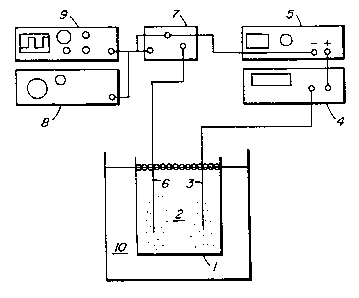
production of nanocrystalline nickel and Figure 1 is a sketch showing a
laboratory
apparatus for carrying the present invention into practice. A plating cell 1,
generally
of glass or thermoplastic construction, contains an electrolyte 2 comprising
an aqueous
acid solution of nickel sulfate, nickel chloride, boric acid and selected
grain size
inhibitors, grain nucleators and stress relievers, to be described in more
detail
hereinbelow. An anode 3 is connected to an ammeter 4 (Beckman, Industrial 310)
in
series connection to a conventional DC Power Source S (S amp, 7S volt max
output).
The anode may be any dimensionally stable anode (DSA) such as platinum or
graphite,
or a reactive anode, depending on the material desired to be deposited.
Preferably, in
the case of nickel deposition, the anode is an electrolytic nickel anode. A
cathode 6 is
connected to the power source S via a transistored switch 7. Cathode b may be
fabricated from a wide variety of metals such as steel, brass, copper and or
nickel, or
non-metal such as graphite. Preferably, cathode 6 is fabricated from titanium
to
facilitate stripping of the nickel deposited thereon. Switch 7 is controlled
by a wave
generator 8 (WaveTEK, Model 164) and the wave form is monitored on an
oscilloscope
9 (Hitachi X212).
The temperature of the electrolyte 2 is maintained in the range between
about SS and 7S° C by means of a constant temperature bath 10 (Blue M
Electric Co.).
A preferred temperature range is about 60-70° C and most preferably
about 6S° C. The
pH is controlled by additions such as Ni,C03 powder or 7:1 H,S04: HCl as
required.
The quality of the deposit and the crystalline structure thereof are
functions of the peak current density in the cell 1, and the rate of pulsing
the current.
Figure 2 illustrates the,maximum current density (I~~) as a function o~ time.
It will be
noted that generally the time off (t°~~) is longer than the time on
(t°~) and that the
current density I~~; may vary between about 1.OA/cm'- and about 3.OA/cm2. The
t°"
may vary between about 1.0 and S.0 msec., with a preferred range of 1.S - 3.0
msec and
an optimum value of 2.S msec. The t°ff may range from about 30 cosec.
to SO cosec. with
an optimum of 4S cosec. It will be appreciated that I~a~, t°" and
t°ff are interrelated and
W~ 94I12~~, ~ ~ ~ ~ ~ , PCT/CA93I00492
. , , .. ..
may be varied within the stated ranges. If the I~a~ is too high, there is a
risk that the
deposited material will burn and, if too low, the grain size will increase.
In all of the following examples, which are illustrative only and not
limiting on the invention, the electrolytic cell described above was employed
with an
electrolytic nickel anode and a titanium cathode and an aqueous electrolyte
(Bath 1)
containing:
Nickel Sulphate (BDI-I) 300 gm/1
Nickel Chloride (BDH) 45 gm/1
Boric Acid (BDH) 45 gm/1 in distilled water. The pH was
adjusted, as noted above, by addition of Ni,C03 powder or 7:1 H, S04: HCI. The
temperature was maintained at GS° C, for a standard plating time of 3
hours. Saccharin
is a known stress reliever and grain refining agent and may be added in
amounts up to
about 10 gm/1. Other stress relievers and grain refining agents which may be
added
include coumarin sodium lauryl sulfate and thiourea. If the bath temperature
rises, it
may be desirable to add a grain size inhibitor such as phosphorous acid in
relatively
small amounts up to about 0.5 - 1 gm/l.
Example 1
Using the apparatus described with reference to Figure 1 and a basic bath
electrolyte composition described above as "Bath 1", 0.5 ,~m/1 saccharin
(Aldrich) was
added and the pH adjusted to pH 2. The I~a~ was 1.9 A/cm'- and t°n was
2.5 m sec. and
to~~ was 45 m sec. The result was a porosity free nanocrystalline nickel
deposit of 0.250 -
0.300 mm thickness with an average grain size of 35 nm.
xam le 2
The procedure and operating conditions of'Example 1 were repeated
except that the saccharin concentration was increased to 2.5 gm/l. 'The result
was a
porosity free deposit of 0.220 - 0.20 mm thickness with an average grain size
of 20 nm.
Example 3
Example 1 was repeated except that the saccharin concentration was
increased to 5 gm/1. The result was a porosity free deposit of 0.200 mm
thickness with
an average grain size of I 1 nm.
6
21~~~~~.5
c:,WO 94/112695
PCT/CA93/00492
~~;~
Example 4
Example 1 was repeated except that the pH was adjusted to pH 4.5 and
the saccharin concentration was increased to 10 gm/l. The result was a
porosity free
deposit of 0.200 - 0.220 mm thickness with an average grain size of 6 nm.
Example S
The products of Examples 1-3 were subjected to hardness testing using a
standard Vickers hardness technique. The results are tabulated in Figure 3 and
illustrate that at the large grain sizes porosity free electroplated nickel
nanocrystals obey
the well established Hall-Petch relationship, i.e. increasing hardness with
decreasing
grain size. However, for the very small sizes of the present invention there
is a clear
deviation from the Hall-Petch relationship indicating a maximum hardness in
the 8 - 10
nm size range.
Example 6
The saturation magnetization of the products of Examples 1-3 was
measured using conventional methods. The results are tabulated in Figure 4 and
compared with the saturation magnetization of gas condensed nanocrystalline
nickel as
reported by Gong et al, supra. It will be noted that while Gong et al report
decreasing
saturation magnetization with decreasing grain size, the products of the
present
invention show very little change in saturation magnetization with grain size
variation,
and even at the smallest grain sizes it is essentially the same as for
conventional nickel.
The nanocrystalline materials of this invention, and particularly
nanocrystalline nickel can be used to provide hard, wear resistant coatings on
many
surfaces. They can also be used as hydrogen storage materials, as catalysts
far hydrogen
evolution and as magnetic materials.
While the invention has been described thus far with reference particularly
to nanocrystalline nickel, the principles thereof are equally applicable to
nanocrystal~ine
soft magnet materials, which are frequently ternary and quaternary iron-nickel
alloys,
and more particularly include Permalloy~' (78.5 Ni 17.1 Fe3.8 Cr. 0.6Mn), Hy
Mu~
(80Ni 16 Fe 4Mo) Supermalloy~' (79Ni 15.7 Fe SMo 0.3Mn) and Mumetal (76Ni l7Fe
SCu 2Cr) (Woldman, Engineering Alloys, 4th Ed, 1962). Other ternary and
quaternary
alloys may contain elements selected from Ni, Fe, Co, Zn, W, Cr, Cu, Mo, Mn,
V, Ti,
Mg, Si, P, C and S. The soft magnetic materials find utility in many
applications but
7
WO 9411269 ~ ~ ~ ~'J'' ~ , FCTICA93140492
are particularly useful for recording head . applications which require high
electrical
resistivity to improve high frequency permeability and to minimize eddy
current losses.
These materials also exhibit good wear characteristics. It has also been found
that,
while useful, pulsed D.C. electroplating is not essential for the production
of
nanocrystalline (<SOnm) nickel-iron alloys such as those described above. D-C
electroplating under carefully controlled conditions has been found adequate.
Example 7 Production of Ternary Nickel-Iron Chromium Alloys
A simple laboratory electroplating bath S 1 (Fig. 5) was placed on a
heating plate ~2. An anode 54, preferably but not essentially, graphite and a
metallic,
preferably copper, cathode ~S were immersed in an electrolyte solution 56 in
bath 51
and connected to a controlled DC power supply 53. The electrolyte comprised an
aqueous solution containing (in grams/litre of solution):
NiCI,~ 50
6H,0
CrCl3~ 0 -
6H,O 100
FeCI,~ 1
4H,0
NaCI 0 -
SO
B(OH)3 25
NH4CI 25
The bath temperature was maintained at a temperature between about 15°C
and about
50°C (preferably room temperature) and the pH of the bath was
maintained in the
range 1-3, depending on the chromium content. At high chromium levels the pH
was
lowered to prevent formation of chromium hydroxide. The current density was
maintained at about 50 mA/sq cm of cathode for periods of time up to about 2
hours
with continuous stirring (0-500 rpm).
In an alternative embodiment using a pulsed D.C. electrolytic cell,
periodic pulse reversal was practised resulting in some grain size ~ reduction
and
improved surface quality. Quality may also be improved using the stress
relievers
previously described and in addition sodium citrate, EDTA, citric acid or
sodium
fluoride.
The composition of the alloy deposited on the copper cathode was
analyzed by energy dispersive x-ray spectroscopy and the results, in terms of
the
chromium concentration of the bath were plotted in Figure 6. It will be noted
that the
8
:'~~VO 94112695 y ~ '~ PCZ'/CA93/00492
~-~» . s
t'r-..# .
chromium content of the alloy is substantially. constant at about 1% but the
nickel
content tends to fall from a maximum of about 86% at 0 g/1 Cr in the bath to a
minimum of about 78% at a concentration of 50 g/I Cr in the bath. Scanning
electron
microscopy indicated that the grain size of the alloy product was less than
100
nanometres while x-ray diffraction studies indicated a grain size of about 10-
15
nanometres with some grain sizes up to about 37 nm.
The electrical, mechanical and magnetic properties of the pure
nanocrystalline nickel products of Examples 3 and 4 have been studied in some
detail,
and it has been determined, somewhat surprisingly in view of previously
published
results (Gong et al J. Appl. Phys. 69, 5119 ( 1991 )) that saturation
magnetization (Ms)
of nanocrystalline nickel produced by the process of examples 2, 3 and 4 is
essentially
independent of grain size. This is, however, consistent with recent
calculations (Szpunar
et al, Condensed Matter Physics, in press) that show that the magnetic moment
of atoms
located in special high angle grain boundaries is only insignificantly
reduced. Even in
an amorphous structure the reduction in Ms is less than 20% and for lOnrn
grain sizes
with an intercrystalline volume fraction of 27%, the overall reduction in Ms
is less than
S%.
Coercivity (Hc) of 50nm nanocrystalline nickel is about 2.0 kA/m which
is about 50% lower than that of conventional polycrystalliipe (100 nm plus)
material (3.0
kA/m). Further reduction in grain size results in an increase in coercivity
back to the
level of the polycrystalline material, which is believed due to the transition
from multi-
domain to single domain grains.
Figure 7 shows that the room temperature electrical resistivity of the
material with a grain size of l lnm is increased by a factor. of three over
the resistivity
value observed for conventional polycrystalline material. At lower
temperatures this
factor increases to approximately five times. This behaviour can be understood
in terms
of electron scattering at the grain boundaries and triple junctions in the
material which
should result in an increase in resistivity with increasing intercrystalline
volume fraction.
This is demonstrated in Figure 8 which shows the excess resistivity as a
function of the
intercrystalline volume fraction for the grain sizes shown in Figure 7. The
excess
resistivity is defined here as the total resistivity minus the resistivity of
conventional
polycrystalline nickel for which the intercrystalline volume fraction is
negligible. The
9
WO 94/12695 ~ 1 ~ g 2 ~- ~ PC'TICA9~100492 ,:
intercrystalline volume fractions in Figure 8 were derived for a grain
boundary thickness
of lnm.
Reduced grain size usually :results in increased hardness as a result of
Hall-Petch strengthening. The Hall-Petch graph for electrodeposited Ni is
shown in
Figure 3. Although there is deviation from linearity far grain sizes less than
3Unm the
important finding is that the hardness of the material is increased by a
factor of S when
reducing the grain size from lUO~m to lUnm.
Using pin-on-disk wear testing under dry conditions an enhancement of
the wear resistance by a factor of four was observed for the same materials.
The corrosion behaviour of nanocn~stalline electrodeposits has recently
been studies by potentiodynamic and potentiostatic testing in a 2N H,S04
solution. As
shown in Figure 9 nanocrystalline nickel exhibits the same active-passive-
transpassive
behaviour as observed in normal crystalline nickel. However the current
density in the
passive range for nanocrystalline materials is higher than for conventional
nickel. This
is believed to be due to the increased defect concentration in the passive
layer on
nanocrystalline material. On the other hand, nanoprocessed Ni did not show the
detrimental type ~of localized corrosion along the grain boundaries which is
usually
observed for conventional nickel. Therefore, although the general corrosion
rate is
somewhat enhanced, the overall excellent corrosion perfor~rtance of nickel is
likely not
sacrificed by nanoprocessing.