Note : Les descriptions sont présentées dans la langue officielle dans laquelle elles ont été soumises.
2~.4~"
... -1-
PROTECTION CIRCUIT FOR ARC DISCHARGE LAMPS
FIELD OF THE INVENTION
This invention relates to arc discharge lamps,
particularly compact fluorescent lamps, and especially to
electronic ballasts containing circuitry for protecting
the lamp from overheating at end-of-life and for
protecting the ballast from component failure.
BACKGROUND OF THE INVENTION
Low-pressure arc discharge lamps, such as
fluorescent lamps, are well known in the art and
typically include a pair of cathodes made of a coil of
tungsten wire upon which is deposited a coating of an
electron-emissive material consisting of alkaline metal
oxides (i.e., BaO, CaO, Sr0) to lower the work function
of the cathode and thus improve lamp efficiency. With
electron-emissive material disposed on the cathode
filament, the cathode fall voltage is typically about 10
to 15 volts. However, at the end of the useful life of
the lamp when the electron-emissive material on one of
the cathode filaments becomes depleted, the cathode fall
voltage quickly increases by 100 volts or more. If the
external circuitry fails to limit the power delivered to
the lamp, the lamp may continue to operate with
additional power being deposited at the lamp cathode
-2-
additional power being deposited at the lamp cathode
region. By way of example, a lamp which normally
operates at 0.1 amp would consume 1 to 2 watts at each
cathode during normal operation. At end-of-life, the
depleted cathode may consume as much as 20 watts due to
the increase in cathode fall voltage. This extra power
can lead to excessive local heating of the lamp and
fixture.
Small diameter (e. g., T2 or ~ inch) fluorescent
l0 lamps generally have very high ignition voltage
requirements necessitating the use of ballasts with open
circuit output voltages which may exceed 1000 volts.
Such voltage levels are enough to sustain a conducting
lamp with an arc drop of 50 to 150 volts with a depleted
cathode and an end-of-life cathode fall voltage of 200
volts. In this example, the lamp would run at nearly
rated current because the excess voltage would be mostly
dropped across the output impedance of the ballast.
Since the cathodes in these small diameter T2 lamps are
placed much closer to the internal tube wall than in
larger diameter lamps, less cathode power is needed to
overheat the glass in the area of the cathode. In such
T2 diameter lamps, it would be desirable to limit the
increase in cathode power to 6 watts in order to avoid
excessive local heating.
For a 6 watt increase in cathode power, the
corresponding RMS lamp voltage increase is only about 52
volts. Normal lamp voltage varies with lamp length,
production variation, cathode heating, ambient
temperature, and fixture effects and can easily vary by
-3-
50 volts or more. For example, the lamp voltage of a
typical 13 watt T2 diameter lamp during normal operation
may vary from 115 volts to 165 volts.
Various attempts have been made to provide over
voltage or over-current protection in inverter-type
ballasts in order to prevent circuit damage due to
excessive load power. For example, U.S. Pat. No.
5,262,699, which issued to Sun et al on November 16,
1993, describes an inverter-type ballast having means for
detecting a relatively large increase in current
resulting from a resonant mode or open circuit (i.e. no
load) condition. The inverter is disabled whenever the
lamp is removed or if the lamp fails to ignite.
Depletion of emissive material on one or more of the lamp
electrodes, which prevents the lamp from igniting, will
cause such an open circuit condition.
U.S. Pat. No. 4,503,363, which issued to Nilssen on
March 5, 1985, describes an inverter-type ballast having
a subassembly which senses the voltage across the output
of the ballast. When an open circuit condition is
detected at the input of the subassembly, resulting from
the removal of a lamp from one of its sockets or the
failure of a lamp to ignite, the inverter is disabled.
While the disabling circuits of U.S. Pat. Nos.
5,262,699 and 4,503,363 may be effective at disabling the
inverter upon detection of a relatively large increase in
current or voltage, these circuits are ineffective at
responding to relatively small increases in cathode fall
power.
"Quicktronic" inverter ballasts manufactured by
21~:~~~~
''. -4 _
OSRAM GmbH for operating "Dulux DE" compact fluorescent
lamps monitor an increase in ballast input power by
sensing supply voltage which is boosted with RF feedback
from the lamp. Effectively, lamp voltage is sensed since
lamp current is somewhat constant in the ballast over the
sense range i.e., voltage=power/current. An increase in
input power of about 6 to 10 watts with a ~2 watt
tolerance is required to disable the inverter. Due to
the drawbacks of voltage sensing as discussed above, this
approach is best suited for sensing very large voltage
increases such as a lamp no start or open circuit load
condition. Moreover, this approach requires tight
control of circuit component tolerances which adds to
cost and reduces load flexibility. Finally, this
approach is not easily adapted to a multiple lamp
configuration because it is difficult to sense lamps
independently.
SUMMARY OF THE INVENTION
It is, therefore, an object of the present
invention to obviate the disadvantages of the prior art.
It is another object of the invention to provide an
inverter disabling circuit which provides lamp and
circuit component protection following a small increase
in lamp voltage resulting from a relatively small
increase in cathode power.
It is still another object of the invention to
provide an inverter disabling circuit which does not
require tight control of circuit component tolerances and
CA 02148399 2004-02-23
77332-158
-5-
which is readily adaptable to multiple lamp configurations.
These objects are accomplished in one aspect of
the invention by the provision of a ballast for a discharge
lamp having a pair of cathodes wherein the discharge lamp is
characterized by a lamp voltage waveform having a DC voltage
component when the lamp approaches end-of-life upon
depletion of emissive material on one of the cathodes. The
ballast comprises an inverter for providing an AC voltage at
a pair of output terminals, means for coupling the discharge
lamp to the output terminals of the inverter, and means for
monitoring the condition of each of the cathodes by
measuring the DC lamp voltage component. The inverter is
disabled after a predetermined increase in the DC lamp
voltage component whereby excessive heating of either
cathode is prevented. The monitoring means preferably
comprises a sensing capacitor for measuring the DC voltage
component of the lamp voltage waveform developing when the
lamp approaches end-of-life. The DC voltage component is
preferably provided to means for disabling the inverter.
In another aspect, the invention provides an
arrangement comprising: a pair of AC input terminals
adapted to receive an AC signal from an AC power supply; DC
power supply means coupled to said AC input terminals for
generating a DC supply voltage; inverter means coupled to
said DC power supply means to receive said DC supply voltage
and including a pair of semiconductor switches, means for
driving said semiconductor switches, and a pair of output
terminals; a discharge lamp coupled to said output terminals
of said inverter means, said discharge lamp having a pair of
cathodes and characterized by a lamp voltage waveform having
a DC voltage component when said lamp approaches end-of-life
upon depletion of emissive material on one of said cathodes;
CA 02148399 2004-02-23
?7332-158
-5a-
means for disabling said inverter after a predetermined
increase in said DC voltage component whereby excessive
heating of said one of said cathodes is prevented; and means
for monitoring a condition of each of said cathodes; wherein
said means for monitoring comprises a sensing capacitor for
measuring the DC voltage component of the lamp voltage
waveform developing when said lamp approaches end-of-life,
and wherein said DC voltage component is provided to said
means for disabling said inverter.
In accordance with further teachings, the
predetermined increase in the DC voltage component is within
the range of from about 3 to 52 volts. Preferably, the
inverter is disabled following an increase in cathode power
of from about 0.3 to 6.0 watts. In a preferred embodiment,
the disabling means includes a full wave bridge rectifier
having an input coupled to the means for monitoring the DC
voltage component.
Additional objects, advantages and novel features
of embodiments the invention will be set forth in the
description which follows, and in part will become apparent
to those skilled in the art upon examination of the
following or may be learned by practice of the invention.
The aforementioned objects and advantages
2~.4$3~~
-6-
may be realized and attained by means of the
instrumentalities and combination particularly pointed
out in the appended claims.
BRIEF DESCRIPTION OF THE DRAWINGS
The invention will become more readily apparent
from the following exemplary description in connection
with the accompanying drawings, wherein:
FIG. 1 is a plot of lamp voltage as a function of
time showing the introduction of a DC component to the
lamp voltage waveform as one lamp cathode wears out;
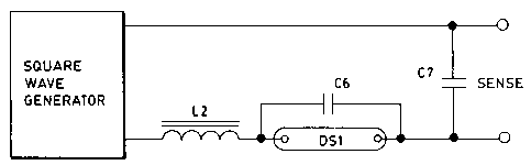
FIG. 2 is a simplified diagram of one method of
series sensing both AC and DC voltages of an arc
discharge lamp;
FIG. 3 is a simplified diagram of another method of
parallel sensing both AC and DC voltages of an arc
discharge lamp;
FIG. 4 is a schematic diagram of one embodiment of
a ballast for a single arc discharge lamp in accordance
with the present invention; and
FIG. 5 is a schematic diagram of another embodiment
of a ballast for multiple arc discharge lamps in
accordance with the present invention.
21~~9~
BEST MODE FOR CARRYING OUT THE INVENTION
For a better understanding of the present
invention, together with other and further objects,
advantages and capabilities thereof, reference is made to
the following disclosure and appended claims in
connection with the above-described drawings.
FIG. 1 is a plot of lamp voltage as a function of
time for one cycle showing the introduction of a DC
to component to the lamp voltage waveform as one lamp
cathode wears out. In a normally operating arc discharge
lamp, as indicated by the waveform lA having an RMS lamp
voltage of 50 volts, the cathode fall voltages of each
cathode are equal. Since the current waveform driving
the lamp, in this example, is symmetrical around the zero
axis, the lamp voltage will contain an AC component and
no DC component. As the lamp approaches end-of-life when
the electron-emissive material on one of the electrode
filaments becomes depleted, the lamp will appear to
partially rectify and a DC component will be added to the
total lamp voltage as indicated by waveforms 1B and 1C.
Due to an increase in cathode fall voltage, the power
consumed by the depleted cathode increases and may lead
to excessive local heating of the lamp and fixture if not
limited.
It should be noted that a depletion of emissive
material on the opposite cathode would also be indicated
by the addition of a DC component (of opposite polarity)
but with a negative increase in the peak voltage
appearing in the second half of the lamp voltage
~14~~~~
_8_
waveform.
In T2 (i.e., ~ inch) diameter lamps, it would be
desirable to limit the increase in cathode power to a
maximum of 6 watts in order to avoid any excessive local
heating. For a larger diameter lamp, the allowable
increase in cathode power may be adjusted accordingly.
In the present example, a 6 watt increase in cathode fall
power corresponds to a change in overall DC lamp voltage
from zero volts to about 52 volts. The present invention
monitors the condition of each lamp electrode by sensing
the DC component in the lamp's voltage waveform
independent of the AC component.
With particular attention to FIG. 2, there is
illustrated a simplified diagram for series sensing both
DC voltage and AC current of an arc discharge lamp
according to one embodiment of the invention. In FIG. 2,
a squarewave generator provides an AC waveform having no
DC component. While a squarewave generator is shown, it
is understood that it may be replaced by a sinewave or
2o other waveform generator. The output of the squarewave
generator in FIG. 2 is connected to a series combination
of an inductor L2, an arc discharge lamp DS1 and a
sensing capacitor C7. A starting capacitor C6 is
connected across lamp DS1. Inductor L2 acts as an AC
impedance to limit current through lamp DS1.
At the end of the useful life of the lamp when the
electron-emissive material on one of the cathode
filaments becomes depleted, the lamp will partially
rectify and a DC voltage component will develop across
capacitor C7. The voltage developed across capacitor C7
-g_
will be equal in magnitude and opposite in polarity to
the DC voltage component across lamp DS1. The value of
capacitor C7 is not critical to the magnitude of the
sensed DC voltage.
Preferably, starting capacitor C6 is two orders of
magnitude smaller than capacitor C7 and is used with
inductor L2 in a resonance circuit to ignite lamp DS1.
If lamp DS1 is off, the squarewave generator sees a
series LC circuit. If the squarewave's fundamental or a
harmonic frequency matches the L2C6 series resonance,
very high resonance currents will flow.
The high current through capacitor C6 develops a
high voltage across capacitor C6 which is used to ignite
the lamp. This high resonant current also passes through
capacitor C7 and develops a high AC voltage thereacross.
In the present embodiment, this AC voltage is used by the
sense circuit to be described below to detect that the
ballast is in a high current resonant starting mode. The
inverter is disabled if the lamp does not ignite within
an acceptable amount of time (e. g., 2-4 seconds).
The value of sense capacitor C7 in FIG. 2 can be
varied to control the magnitude of the sensed AC voltage
independent of any DC component discussed earlier. Sense
capacitor C7 has independent AC and DC voltage components
which are used by shutdown circuitry 20. The sensed DC
voltage component is used to trigger shutdown circuitry
20 and thereby disable the ballast in response to
detection of a rectifying lamp as the lamp approaches
end-of-life. Alternatively, the shutdown circuitry is
triggered by the sensed AC voltage component if the lamp
-10-
does not light or if the lamp is removed from the circuit
or, in other words, an open circuit condition or high AC
lamp voltage is detected.
Capacitor C6 is not necessary if the output voltage
of the squarewave generator is high enough to light the
lamp or if some other starting means is used. In this
case, only the DC voltage of capacitor C7 needs to be
monitored.
FIG. 3 illustrates a simplified diagram for
parallel sensing both AC and DC voltages of an arc
discharge lamp according to another embodiment of the
invention. In FIG. 3, the output of the squarewave
generator is connected to a series combination of an
inductor L2, an arc discharge lamp DS1 and a capacitor
C7. A series combination of capacitors C6 and C20 is
connected across arc discharge lamp DS1 to provide
resonant starting. A resistor R20 is connected in
parallel with capacitor C6.
Capacitors C6 and C20 form an AC voltage divider
which provides an AC voltage across capacitor C20 that is
proportional to the AC lamp voltage. Capacitor C6 is
generally smaller than capacitor C20 by an order of
magnitude so resonant calculations must include the
effect of capacitor C20.
Simple inverter-type circuits employing, for
example, a two transistor squarewave inverter, often
generate an undesired DC output voltage component. In
the approach illustrated in FIG. 2 this error voltage
develops across capacitor C7. However, if the
transistors of the inverter are well matched, this error
-11-
voltage will be relatively small. In the approach
illustrated in FIG. 3, any error voltage will develop
across capacitor C7 and will not affect the sense output.
Capacitor C7 in FIG. 3 is optional and can be used to
block any DC voltage which may be present at the output
of the squarewave generator. If desired, capacitor C7
may be eliminated.
At the end of the useful life of the lamp when the
electron-emissive material on one of the cathode
filaments becomes depleted, the lamp will partially
rectify and a DC voltage component will develop across
capacitor C20 in FIG. 3. The voltage developed across
capacitor C20 will be equal in magnitude and polarity to
the DC voltage component across lamp DS1. The value of
capacitor C20 is not critical to the magnitude of the
sensed DC voltage.
FIG. 4 represents a schematic diagram of a
preferred embodiment of a ballast for a discharge lamp
DS1. Lamp DS1 is an arc discharge lamp such as a low-
pressure fluorescent lamp or a high-pressure high
intensity discharge lamp having a pair of opposing
filamentary cathodes E1, E2. Each of the filamentary
cathodes is coated during manufacturing with a quantity
of emissive material. Lamp DS1, which forms part of a
load circuit 10, is ignited and fed via an oscillator 12
which operates as a DC/AC converter. Oscillator 12
receives filtered DC power from a DC power supply 18
which is coupled to a source of AC power. Conduction of
oscillator 12 is initiated by a starting circuit 14. In
order to prevent excessive heating of the cathodes,
214
-12-
circuit 20 temporarily disables the oscillator upon
detection of a lamp which is approaching the end of it's
useful life and is beginning to rectify. In a preferred
embodiment, circuit 20 will also temporarily disable the
oscillator upon detection, for example, of a completely
failed lamp (i.e., no current flow therethrough) and a
removed lamp.
A pair of input terminals IN1, IN2 are connected to
an AC power supply such as 108 to 132 volts, 60 Hz. A
fuse F1, a circuit breaker CB1 and a varistor RV1 are
connected in series across input terminals IN1, IN2 in
order to provide over current, thermal and line voltage
transient protection, respectively.
A network 16 consisting of an inductor L1, a pair
of capacitors C11 and C12, and a resistor R17 is
connected in series with input terminal IN1 and the input
of a DC power supply 10. Network 16 forms a third order,
damped low-pass filter that waveshapes the AC input
current so as to increase the power factor and lower the
total harmonic distortion the input of the DC power
supply presents to the AC power supply. Details of this
network can be found in U.S. Pat. No. 5,148,359 which
issued to Ngyuyen.
DC power supply 18 consists of a voltage doublet
arrangement which includes a pair of diodes D1 and D2 and
a pair of capacitors C2 and C3. Capacitors C2 and C3 are
shunted by resistors R14 and R15, respectively.
Resistors R14 and R15 safely discharge capacitors C2 and
C3 when power is off and also allow for the quick
resetting of the shutdown circuit by discharging the
~~~p399
-13-
latching operation in about 2.5 seconds. A pair of
capacitors C1 and C11 together with inductor L1 provide
EMI noise filtering.
Oscillator 12, which includes (as primary operating
components) a pair of series-coupled semiconductor
switches, such as bipolar transistors Q1, Q2 or MOSFETS
(not shown), is coupled in parallel with output terminals
+VCC and -VCC of DC power supply 18. The collector of
transistor Q1 is connected to terminal +VCC. The emitter
is connected to one end of a resistor R4. The other end
of resistor R4 is connected to the collector of
transistor Q2. The emitter of transistor Q2 is coupled
to terminal -VCC through a resistor R6.
Base drive and switching control for transistors Q1
and Q2 are provided by secondary windings Tla and Tlb of
a saturable transformer and base resistors R3 and R5,
respectively. A pair of flyback diodes D7 and D8 direct
energy stored in inductor L2 back into the power supply
capacitors C2 and C3 when both transistors Q1 and Q2 are
2o not conducting.
Oscillator starting circuit 14 includes a series
arrangement of resistors R1, R13 and R16 and a capacitor
C5. The junction point between resistor R1 and capacitor
C5 is connected to a bi-directional threshold element CR1
(i.e., a diac). One end of threshold element CR1 is
coupled to the base or input terminal of transistor Q2.
During normal lamp operation, oscillator starting
circuit 14 is rendered inoperable due to a diode
rectifier D3 by holding the voltage across starting
capacitor C5 at a level which is lower than the threshold
-14-
voltage of threshold element CR1.
A pair of resistors R2 and R9 and a capacitor C4
form a snubber network to reduce transistors switching
losses and to reduce EMI noise conducted back into the
power line.
Load circuit 10 comprises a parallel combination of
a capacitor C6 and lamp DS1 in series with primary
winding Tlc, an inductor L2 and a capacitor C7.
Typically, the transistor switching frequency is from
about 20 Khz to 60 Khz. The terminals T1, T2 of
discharge lamp DS1 may be coupled to capacitor C6 by
means of suitable sockets in order to facilitate lamp
replacement. Although FIG. 4 illustrates an instant-
start discharge lamp wherein the lead-in wires from each
cathode are shorted together and coupled to respective
terminals, other coupling arrangements are possible.
In the embodiment illustrated in FIG. 4, circuit 20
includes a full wave bridge rectifier network consisting
of diodes D4a, D4b, D5a and DSb. This rectifier network
permits detection of a DC voltage of either polarity, the
polarity of which depends upon the cathode that becomes
depleted of emissive material. A series combination of a
resistor R8 and a capacitor C9 is connected across diodes
D4a and D4b and provides a low pass filter with a time
constant of, for example, about 0.5 second. Resistor R8
and capacitor C9 filters out lamp voltage transients
which occur normally, for example, during starting when
very high resonant currents are passing through capacitor
C7. A resistor R10 shunting capacitor C9 discharges
capacitor C9 when the sensed voltages are low allowing
-15-
the shutdown circuit to reset, for example, after a
start. Resistors R8 and R10 also provide for voltage
division to set the trip level of the sensed DC voltage.
Moreover, these resistors divide the AC sensed voltage
which can be further independently adjusted by changing
the value of capacitor C7.
Circuit 20 further includes an optical isolator IC1
having an input terminal (pin 1) connected to a series
combination of a bi-directional threshold element CR2 and
a resistor R7. The other input terminal (pin 2) of
optical isolator ICl is connected to the negative
terminal of capacitor C9. One of the output terminals
(pin 4) of optical isolator IC1 is connected to output
terminal -VCC of DC power supply 18. The other output
terminal (pin 3) is connected to one end of a diode D6.
The other end of diode D6 is coupled through a resistor
R11 to the base or input terminal of transistor Q1. A
series combination of a resistor R12 and a capacitor C10
is connected to the output terminals of optical isolator
IC1.
The current waveshape through lamp DS1 is
approximately a sinewave and only varies ~4% over the
acceptable rectifying lamp voltage range. Assuming a
constant sinewave of lamp current and a sinewave of lamp
voltage, the following shutdown relations can be
developed:
Pcath-~x* Ramp * Vdc/(2 * SQR(2))~
3o Vtrip ((R8+R10)*VCS/R10-ICS/(n*F*C7*SQR(2)~Vtcc*F*~tSl+1)
-16-
where:
Pcath=Rectifying cathode fall field power increase in watts.
It=3.14159
Il~p RMS current through the lamp in amperes.
Vd~ The rectifying cathode DC voltage in volts.
SQR=The square root of (...)
Vt~p The DC voltage where the shutdown circuit will activate in volts. A
window is defined by using the minimum and maximum parameter values. If
Vtrip<0,
to then Vtrip 0. When Vdc = or < Vtrip, the ballast shuts down.
R8 and R10=Circuit voltage divider resistors in ohms.
VCS=The firing voltage of solid state switch CR2 in volts.
ICS=Resonating current through capacitor C7 in amperes. Approximately
equals the lamp current when the lamp is on.
F=Ballast oscillating frequency in HZ.
C7=Circuit sensing capacitor in Farads.
Vtcc Supply voltage from -Vcc to +Vcc in volts.
~tsi The difference between the storage times in seconds of transistors Q 1
and Q2.
It should be noted that the power increase in the
dying cathode is directly proportional to the magnitude
of the measured DC voltage across the lamp. Since either
polarities of DC voltages is monitored by the sensing and
disabling circuit due, in part, by the full wave bridge
rectifier D4a, D4b, D5a and DSb, failure of either
cathode will cause the oscillator to be disabled.
The activation voltage of circuit 20 is directly
proportional to several parameters. The tolerances of
these parameters define a sensing window for a family of
-17-
ballasts that monitor the failure of either cathode or a
high resonant current starting mode. It is desirable to
use transistors that are closely matched or operate at a
lower frequency to minimize the Otsi effect of transistor
differences. Base drive and collector loading must also
be matched or ~tsi will be increased. Differences in
transistor heating can cause ~tsi to increase. For
example, external transistor case heating can cause Otsi
to increase up to 1 volt per °C difference between the
transistors. It is desireable for the transistors to be
in physical contact with one another to minimize
temperature differences.
In the example ballast illustrated in FIG. 4, the
oscillating frequency is about 50 KHZ and the unselected
transistor mismatch is 300 nanoseconds maximum. This
results in a sensed mismatch error voltage of under ~5
volts DC which corresponds to a cathode power sensing
error of ~0.5 watt. The other parameters are selected to
provide a trip window range of 13.7 to 35.9 volts which
yields a 1.5 to 3.8 watts possible cathode increase at
100 mA of lamp current. The maximum acceptable window,
noted earlier for the T2 diameter lamp, is within the
range of from about 3 to 52 volts which yields a 0.3 to
6.0 watt possible rejectable cathode increase range at
100 mA of lamp current.
It should also be noted that the activation voltage
of circuit 20 is proportional to the current through
capacitor C7. This current is approximately equal to the
lamp's current when the lamp is on and can be considered
a constant. While the lamp is starting or out of the
-18-
circuit, this current will equal the very large resonant
starting current through capacitor C6. This causes the
lower side of the trip window to move towards 0 volts as
capacitor C9 charges'and the ballast will shut down when
Vtrip-0 after a delay if the lamp does not start.
Setting Vtrip- 0, allows for the calculation of ICS which
is independent of Vdc. With the values used in the
embodiment, the nominal shut down resonating current is
210 mA or about twice the rated lamp current.
l0 The operation of the ballast will now be discussed
in more detail. When terminals IN1 and IN2 are connected
to a suitable AC power source, DC power source 18
rectifies and filters the AC signal and develops a DC
voltage across capacitors C2 and C3. Simultaneously,
starting capacitor C5 in oscillator starting circuit 14
begins to charge through resistors R1 and R13 to a
voltage which is substantially equal to the threshold
voltage of threshold element CR1. Upon reaching the
threshold voltage (e. g., 32 volts), the threshold element
breaks down and supplies a pulse to the input or base
terminal of transistor Q2. As a result, current from the
DC supply flows through resistor R6, the collector-
emitter junction of transistor Q2, primary winding Tlc,
inductor L2 and capacitors C6 and C7. Since the lamp is
essentially an open circuit during starting, no current
flows through the lamp at this time. Current flowing
through primary winding Tlc causes saturation of the
transformer's core which forces the inductance of the
transformer to drop to zero. A resulting collapse in the
magnetic field in the transformer causes a reverse in
-19-
polarity on secondary windings Tla and Tlb. As a result,
transistor Q2 is turned off and transistor Q1 is turned
on. This process is repeated causing a high voltage to
be developed across capacitor C6 (and lamp DS1) as a
result of a series resonant circuit formed by capacitors
C6, C7 and inductor L2. The high voltage developed
across capacitor C6 is sufficient to ignite lamp DS1.
At the end of the useful life of the lamp when the
electron-emissive material on one of the cathode
to filaments becomes depleted, the lamp will partially
rectify and a DC voltage component will develop across
capacitor C7 in FIG. 4. The voltage developed across
capacitor C7 will be equal in magnitude and opposite in
polarity to the DC voltage component across lamp DS1.
The value of capacitor C7 is not critical to the
magnitude of the sensed DC voltage.
The voltage developed across capacitor C7 is
rectified by diodes D4a, D4b, D5a and D5b and filtered by
capacitor C9. Resistors R8 and R10 provide for voltage
division to set the trip level of the DC voltage measured
across capacitor C7.
Resistors R8 and R10 also divide the AC sensed
voltage which can be further independently adjusted by
changing the value of capacitor C7. By properly
adjusting resistors R8, R10 and capacitor C7, the shut
down circuit 20 can be adapted to also disable the
oscillator in the event the lamp does not light or if the
lamp is removed from the circuit.
When the voltage across capacitor C9 reaches the
threshold voltage of switch element CR2, optical isolator
-20-
threshold voltage of switch element CR2, optical isolator
IC1 is triggered causing shunting of the output terminals
(pins 3 and 4) of IC1 and coupling of the base of
transistor Q1 to -VCC. Because of the limited voltage
available at the base of transistor Q1, the base drive
current will be insufficient to turn on transistor Q1,
causing an interruption in operation of the oscillator.
With the ballast shut down, no signal is supplied to
capacitor C9 which begins to discharge through resistor
R10. The output of IC1 (at pins 3 and 4) remains shunted
maintaining transistor Q1 biased off and the ballast in a
shutdown state. The output of IC1 contains a latching
solid state switch (a triac) which receives latching
current from +VCC through resistors R2 and R9 and from
terminal IN1 through resistors R1 and R13.
After power to the ballast is disconnected, the
voltage across capacitors C2 and C3 begin to discharge
through discharge resistors R14 and R15. The circuit is
reset and conduction of transistors Q1 and Q2 is
restarted by reconnecting power to the ballast after
allowing the voltage across capacitor C9 to drop
sufficiently that the holding current level of IC1's
output triac (pins 3 and 4) is not maintained. It is
possible to modify circuit 20 for example, with a non-
latching optical isolator, so that it would not be
necessary to disconnect power to the ballast in order to
reset the shut down circuit.
If switch CR1 fails to turn on during starting, the
inverter will not oscillate. To disable turn on of
switch CRl, a resistor R16 is preferably connected across
-21-
and R13 across DC power supply 18.
If the ballast is connected to an AC line voltage
of less than 90 volts, capacitor C5 will not charge to a
voltage sufficient to cause switch CR1 to turn on and the
inverter of the ballast will be disabled. Moreover, if
the ballast is on when the line voltage is reduced, and
the shutdown circuit momentarily turns off the inverter
but does not latch off the inverter due to insufficient
holding current through the triac of IC1, the circuit
could restart without resistor R16 and flash on and off.
However, with resistor R16, the ballast stays off, i.e.,
does not restart. Resistor R16 also provides for low
line voltage shutdown.
FIG. 5 illustrates a two lamp circuit diagram
demonstrating independent shutdown with multiple lamps
DS1, DS2. The input side of each shutdown circuit 20 and
22 is duplicated for each lamp while the output side is
common. Optical isolators IC1 and IC2 separate the input
and output sides. Separate sensing capacitors C7 and C13
provide for independent lamp sensing. The shut down
performs as noted above, however, failure of either lamp
will shut down the ballast and extinguish both lamps.
Although only two lamps are shown, it is within the scope
of the invention to include any suitable number of lamps.
As a specific example but in no way to be construed
as a limitation, the following components are appropriate
to the embodiment of the present disclosure, as
illustrated by FIGS. 4 and 5:
2~4~~~
-22-
Item Type Schematic Value
C1 Capacitor (ceramic) 0.022 MFD
C2 Capacitor (electolytic) 33 MFD
C3 Capacitor (electrolytic) 33 MFD,
C4 Capacitor (ceramic) 330 PF
C5 Capacitor (ceramic) 0.047 MFD
C6 Capacitor (ceramic) 0.0022 MFD
C7 Capacitor (ceramic) 0.022 MFD
C9 Capacitor (electrolytic) 10 MFD
C10 Capacitor (ceramic) 0.022 MFD
C11 Capacitor (film) 0.5 MFD
C12 Capacitor (film) 1 MFD
C13 Capacitor (ceramic) 0.022 MFD
C14 Capacitor (ceramic) 0.0022 MFD
C15 Capacitor (electrolytic) 10 MFD
CB1 Thermal Breaker 100 C
CR1 Diac 32 Volts
CR2 Diac 32 Volts
CR3 Diac 32 Volts
D1 Diode 1N4249
D2 Diode 1N4249
D3 Diode GL34J
D4a Diode (~) CMPD2004S
D4b Diode (~) CMPD2004S
D5a Diode (~) CMPD2004S
D5b Diode (~) CMPD2004S
D6 Diode 1N4937GP
D7 Diode 1N4937GP
D7a Diode (~) CMPD2004S
D7b Diode (~) CMPD2004S
D8 Diode 1N4937GP
D8a Diode (~) CMPD2004S
D8b Diode (~) CMPD2004S
DS1 Fluorescent 20 inches
Lamp
DS2 Fluorescent 20 inches
Lamp
F1 Fuse 3 Amps
214~~~
IC1 Opto/triac TLP525G
IC2 Opto/Triac TLP525G
L1 Inductor 500 mH
L2 Inductor 4.0 mH
L3 Inductor 4.0 mH
Q1 NPN Transistor BULK26
Q2 NPN Transistor BULK26
R1 Resistor 220 K ohm
R2 Resistor 220 K ohm
R3 Resistor 33 ohm
R4 Resistor 2.7 ohm
R5 Resistor 33 ohm
R6 Resistor 2.7 K ohm
R7 Resistor 330 ohm
R8 Resistor 47 K ohm
R9 Resistor 220 K ohm
R10 Resistor 150 K ohm
R11 Resistor 330 ohm
R12 Resistor 330 ohm
R13 Resistor 220 K ohm
R14 Resistor (FIG. 4) 470 K ohm
R15 Resistor (FIG. 4) 470 K ohm
R16 Resistor (FIG. 4) 82 K ohm
R14 Resistor (FIG. 5) 330 K ohm
R15 Resistor (FIG. 5) 150 K ohm
R16 Resistor (FIG. 5) 47 K ohm
R17 Resistor 50 ohm
Tla Transformer 3 Turns
Tlb Transformer 3 Turns
Tlc Transformer 5 Turns
VR1 MOV 150 VAC
There has thus been shown and described an inverter
disabling circuit which provides lamp and circuit
component protection following an increase in lamp
voltage resulting from a relatively small increase in
-24-
cathode power. The disabling circuit does not require
tight control of circuit component tolerances and is
readily adaptable to multiple lamp configurations.
While there have been shown and described what are
at present considered to be the preferred embodiments of
the invention, it will be apparent to those skilled in
the art that various changes and modifications can be
made herein without departing from the scope of the
invention.