Note : Les descriptions sont présentées dans la langue officielle dans laquelle elles ont été soumises.
21~15~7
TITI,~
LIQUID CRYSTAL DEVICE AND PROCESS FOR PREPARING THE SAME
The present invention relates to a liquid crystal
device used for conducting optical modulation in various
fields such as optical communication, stereoscopic image
display, image processing, optical operation and plain
image display, and to a process. for preparing said device.
1~ More particularly, the invention relates to a liquid
crystal device using electrooptic effect of the smectic
liquid crystal phase and to a process for preparing said
device.
B_A_CKGROUND OF THF INVENTInN
In order to lighten various optical modulation devices
and display devices or to reduce power consumption required
for these devices, a tendency of using liquid crystal
devices for these devices has been recently increased. Of
various liquid crystal devices, ferroelectric or
antiferroelectric liquid crystal devices using electrooptic
effect of a smectic liquid crystal phase (hereinafter
referred to as "smectic liquid crystal device") have been
paid attention because they have a wider view angle of
field and a higher response speed as compared with TN
liquid crystal devices. Particularly because the
antiferroelectric crystal devices are excellent in impact
resistance and almost free from a problem of printing a
21515~'~
2
liquid crystal material on the inner surface of a liquid
crystal cell, they have been recently paid much attention.
The smectic liquid crystal device includes a liquid
crystal cell in whir_h a liquid crystal material capable of
S exhibiting a smectic liquid crystal phase (hereinafter
referred to as "smectic liquid ~~rystal material") with a
thickness of not more than several ~t.m is filled between
electrodes provided on a pair o:E substrates, and also
includes, if necessary, various polarization control means.
For conducting optical modulation with a sufficiently high
contrast using the device, a layer of the smectic liquid
crystal material in the liquid crystal cell is desired to
be uniformly orientated so that the layer normal directions
of the smectic liquid crystal (normal directions against
the smectic liquid crystal layer) shown in Figs. 3-A, 3-B
and 3-C are almost the same as Each other. In these
figures, the liquid crystal molecules are orientated in
such a manner that each liquid crystal molecule has a tilt
angle 8, to form a liquid crystal layer. The layer normal
2 0 shown in Fig. 3 is parallel with the electrode surface of
the liquid crystal cell. In Fic~. 3-A, a liquid crystal
layer formed from liquid crystal. molecules whose every
spontaneous polarization is in the upward direction and a
liquid crystal layer formed from liquid crystal molecules
whose every spontaneous polarization is in the downward
direction are layered one upon another. In Fig. 3-B,
liquid crystal layers each formed from liquid crystal
molecules whose every spontaneous polarization is in the
21515~~
3
upward direction are layered on~~ upon another. In Fig. 3-
C, liquid crystal layers each f~~rmed from liquid crystal
molecules whose every spontaneous polarization is in the
downward direction are laminated one upon another.
S Particularly in the case o:E optical switches for
optical communication, optical abutters for stereoscopic
image display and spatial optical modulators used for image
display, image processing and optical operation, a contrast
of at least about 100 is necess<~ry, so that it is required
that not only the smectic liquid crystal layer is uniformly
orientated all over the device surface but also occurrence
of various defects in the smect_~c liquid crystal layer is
inhibited.
For making the layer norma~_ directions of the smectic
liquid crystal the same as each other, there is
conventionally known a method of= first forming an
orientation film made of a polymer thin film such as a
polyimide thin film on the interface between the substrate
and the liquid crystal material and then subjecting the
2 0 orientation film surface which i.s to be brought into
contact with the liquid crystal material to a rubbing
treatment. The term "rubbing treatment" used herein means
a treatment of rubbing the surfa:ce of the orientation film
formed on the substrate in a given direction with a cloth
or the like.
When the liquid crystal material is filled between the
orientation films whose rubbing directions are parallel
with each other, however, plural domains having layer
2:~51~6'~
4
normal directions of the smectic liquid crystal different
from those of their adjacent domains are often formed.
Especially in the case where the layer normal directions of
the smectic liquid crystal are ;strikingly different with
domains, if electric voltage is applied to the liquid
crystal cell to change the orientation state of the smectic
liquid crystal layer inside the liquid crystal cell, light
leaking takes place because the extinction positions of the
smectic liquid crystal layer dii=fer with domains.
Therefore, the liquid crystal device provided with such a
liquid crystal cell as mentioned above has a problem that
the contrast between brightness and darkness of the output
lights before and after optical modulation ~is conducted by
this liquid crystal device becomes smaller as compared with
the case of using a liquid crystal device in which the
layer normal directions of the ;~mectic liquid crystal
present inside the liquid crystal cell are the same as each
other. That is, a sufficiently high contrast cannot be
obtained by the use of a ferroel.ectric or antiferroelectric
liquid crystal device provided with a liquid crystal cell
in which a liquid crystal material is filled between such
orientation films as have rubbing directions parallel with
each other.
For solving this problem, particularly in the
antiferroelectric liquid crystal device, there have been
proposed methods of shifting the rubbing direction against
the orientation film formed on each of the upper and lower
substrates. For example, Japanese Patent Laid-Open
2)~51~G'~
s
Publication No. 371925/1992 proposes a method of shifting
the rubbing direction by the sum (61 + 62) of the angle 61
which is formed by the rubbing direction and the layer
normal of the liquid crystal in a smectic A phase on the
surface of the orientation film provided on the upper
substrate and the angle 62 which. is formed by the rubbing
direction and the layer normal of the liquid crystal in a
smectic A phase on the surface of the orientation film
provided on the lower substrate., Japanese Patent Laid-Open
Publication No. 3676/1994 proposes a method of shifting the
rubbing direction by a given angle.
However, the method proposed in Japanese Patent Laid-
Open Publication No. 371925/1992 is not applicable because
the angle between the rubbing directions on the surfaces of
the orientation films formed on the upper and lower
substrates cannot be determined in the case of a liquid
crystal material whose layer normal against the rubbing
direction is not decided univocally or a liquid crystal
material which cannot be in a smectic A phase.
2 0 Also in the method proposect in Japanese Patent Laid-
Open Publication No. 3676/1994, there is a problem that the
preferred range of the angle to obtain sufficiently uniform
orientation is not always clear.
In the above-mentioned conventional methods, moreover,
2s stripe defects induced by application of an electric field
cannot be inhibited, and hence when switching between the
ferroelectric states, which is brought about by applying
electric voltage to the antiferroelectric liquid crystal
21 51as~
device, is used for the optical modulation, a sufficiently
high contrast can be hardly obtained only by shifting the
rubbing direction of the surface of the orientation film
formed on each of the upper and lower substrates by
application of an electric field.
OBJECT OF THE INVENTION
The present invention is intended to solve such
problems associated with the prior art as mentioned above,
and it is an object of the invention to provide a liquid
crystal device which can conduct optical modulation with a
high contrast using electrooptic effect of the smectic liquid
crystal phase and to provide a process for preparing said
device.
It is another object of the invention to provide a
liquid crystal device which can inhibit stripe defects
occurring in the course of driving the liquid crystal device
thereby to conduct optical modulation with keeping the state
of high contrast and to provide a process for preparing said
device.
SUMMARY OF THE :CNVENTION
The liquid crystal devicE~ (or element) according to
the present invention comprises a :Liquid crystal cell filled
with a liquid crystal material capable of exhibiting a
smectic phase. The cell includes upper and lower substrates
each having an electrode and an orientation film on a surface
of the electrode, in which the surface of each orientation
film in contact with the liquid crystal material has been
subjected to an orientation treatment in a direction to
72932-207
21 51567
7
control an orientation direction o:E the liquid crystal
material contacted thereto, and the=_ orientation treatment
direction of one orientation film :is different from the
orientation treatment direction of the other orientation film
such that a cross angle formed by those orientation treatment
directions of the orientation film;, as measured in the
clockwise direction based on the orientation treatment
direction of the orientation film of the upper substrate
side, is represented by the following formula [I] or [II]
to a = lso° - s [I]
360° - b [II]
wherein 0° < b <_ 90°
In this liquid crystal device, it is preferred
that:
(a) when the liquid crystal cell filled with the
liquid crystal material in a smect_~c phase is placed between
two polarizing plates of the crossed Nicols arrangement in
such a manner that the amount of tree transmitted light, which
transmits through one polarizing p7_ate, the liquid crystal
20 cell and the other polarizing plate in this order, would be
minimum, the minimum value T of the light transmittance
represented by the following formu7_a [IV] is not more than
1.0 %~
o,
T = [ (I-IO) /I100] x 100 [IV]
wherein I is the minium amount of t:he transmitted light, IO
is an amount of the transmitted light in the crossed Nicols
arrangement when the liquid crystal. cell is not
72932-207
2~~~~~"~
s
placed, and Iloo is a difference between Io and the amount
of the transmitted light in the parallel Nicols arrangement
when the liquid crystal cell is not placed;
(b) when the liquid crystal. cell filled with the
S liquid crystal material in a smectic phase is placed
between two polarizing plates of the crossed Nicols
arrangement in such a manner that the amount of the
transmitted light, which transmits through one polarizing
plate, the liquid crystal cell a.nd the other polarizing
1~ plate in this order with applying electric voltage between
the electrodes of the liquid crystal cell to vary the
optical axis of the cell, would be minimum, the minimum
value T' of the light transmitta.nce represented by the
following formula [V] is not more than 1.0 0;
IS T' - [ (I'-Io) /Iloo] x 100 [V]
wherein I' is the minimum amount of the transmitted light,
Io is an amount of the transmitted light in the crossed
Nicols arrangement when the liquid crystal cell is not
placed, and Iloo is a difference between Io and the amount
2 ~ of the transmitted light in the parallel Nicols arrangement
when the liquid crystal cell is not placed; or
(c) when the liquid crystal cell filled with the
liquid crystal material in a smectic phase is placed
between two polarizing plates of the crossed Nicols
2S arrangement in such a manner that the amount of the
transmitted light, which transmits through one polarizing
plate, the liquid crystal cell and the other polarizing
plate in this order after alternating voltage is applied
21 515 87
9
between the electrodes of the liquid crystal cell to drive
the cell and application of the voltage is stopped, would be
minimum, the minimum value T" of t:he light transmittance
represented by the following formula [VI] is not more than
1.0 %~
o,
T" - [ (I"-IO) /I100] x 100 [VI]
wherein I" is the minimum amount o:E the transmitted light, IO
is an amount of the transmitted light in the crossed Nicols
arrangement when the liquid crystal cell is not placed, and
1100 is a difference between IO and the amount of the
transmitted light in the parallel l~licols arrangement when the
liquid crystal cell is not placed.
The present invention al:~o provides a process for
preparing a liquid crystal device having a liquid crystal
cell filled with a liquid crystal material capable of
exhibiting a smectic phase and including upper and lower
substrates each having an electrode and an orientation film
on a surface of the electrode. The process comprises a step
of subjecting a surface of each or_Lentation film to an
orientation treatment in a direction to control an
orientation direction of a liquid crystal material contacted
thereto. The orientation treatment: is conducted in such a
manner that the cross angle formed by the orientation
treatment direction of one orientation film and the
orientation treatment direction of the other orientation film
in the cell, as measured in the clockwise direction based on
the orientation treatment direction of the orientation film
of
72932-207
10
the upper substrate side, would be an angle represented by
the following formula [I] or [II]:
A = 180° - 8 [I]
A = 360° - 8 [II]
S wherein 0° < $ < 90°.
In the process for preparing a liquid crystal device
according to the invention, it is preferred that:
the liquid crystal material in an isotropic phase is
cooled to conduct phase transition of from the isotropic
phase to a smectic phase while electric voltage larger in
the absolute value than that required for varying the
optical axis of the liquid crysi:al material when the liquid
crystal material is in a smectic phase is applied between
the electrodes of the liquid crystal cell; or
electric voltage larger in the absolute value than
that required for varying an opi~ical axis of the liquid
crystal material when the liquid crystal material is in a
smectic phase is applied between the electrodes of the
liquid crystal cell.
BRIEF DESCRIPTION OF THE DRAWIN
Fig, 1 schematically illustrates one example of the
liquid crystal devices according to the present invention.
Figs. 2-A-1, 2-A-2, 2-B-1 and 2-B-2 each schematically
illustrates rubbing directions of the orientation films in
the liquid crystal device shown in Fig. 1.
Figs. 3-A, 3-B and 3-C illustrate various orientation
states of the liquid crystal material in a smectic phase
21 51567
11
f i 1. led i nsi~ie the smect i.c L i.<yii.cl cr_ysta.l cell of the 1 i.qoid
crystal device according to the present invention.
UET'11ILED_ UE~( fyIPTIC~N~E_'_ Tt-tE INVEN'I'IQN
S [I~:i.qui_d crystal. device]
First, the liquid crystal. device according to the
invention is described with reference to the attached
drawings.
E'ig. 1 shows one example of the 1i_qui.d crystal device
LU accordi.ng to the invent.i.on .
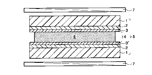
The liquid crystal device comprises a liquid
crystal cell 5 which has a pair of substrates 1,1,
electrodes ?.,2 forrned on the surfaces of both substrates
1,1, an orientation film 3 formed on one electrode 2, an
l.S ori_eutation fi lm 3' formed on tine other electrode 2, and in
the cell 5 a liquid crystal material 6 is filled i.n a gap 4
between the orientation films 3,3'.
'1'Lre sut~:,tr_<~t_e L is, for_ exarnLol.e, a t.rarrsparent glass
plate, a transparent: plastic plate or a transparent plastic
2 ~ film. Examples of t:he transparent glasses include soda-
lime glass" borosilicate glass, non-alkali glass and
quartz. Examples of the transparent plast=i_cs include
polyolefin, polyester and polystyrene. When other glass
plate than a quartz plate, the transparent plastic plate or
25 the transparent plastic film is used as the substrate 1, it
is preferred to pre iminarily form an ~zndercoat (not shown)
such as a S.i_OZ film on tree substrate 1_ by means of cii.p
coating, deposition or sputtering and then forming thereon
72932-207
;015.15~"~
12
the electrode 2, to prevent elution of impurities contained
in the substrate l, such as metallic ion and stabilizer,
into the liquid crystal material 6.
In the liquid crystal device 10, a conductive film
which is transparent to (transmits) such a light of
wavelength as is modulated by the liquid crystal device 10
is used as each of the electrodes 2,2. Examples of such
conductive films include an indium tin-oxide conductive
film (known as "ITO") and a zinc' oxide conductive film.
The conductive film is formed on the substrate 1 by means
of, for example, dip coating, CVD method, sputtering, ion
plating or vacuum deposition.
In the present invention, it is enough'that at least
one of the electrodes 2,2 is transparent to such a light of
wavelength as is modulated by the liquid crystal device 10.
When one electrode 2 is transparent to such a light of
wavelength as is modulated by th,e liquid crystal device 10,
the other electrode 2 can be selected from electrodes of
various types according to the u.se application of the
liquid crystal device 10. For example, the above-mentioned
transparent electrode or an elecarode obtained by forming a
photoconductive layer such as a layer of amorphous silicon
or CdSe on the transparent electrode can be employed. In
the latter case, when electric voltage is applied between
the transparent electrodes, the intensity of electric field
formed in the liquid crystal material between the
orientation films 3,3' varies according to the intensity of
the light with which the photoconductive layer is
21 51567
13
irradiated. Utilizing the characteristics, for example, the
polarization state of the reflected light of a light which
enters from the side of the substrate having only a
transparent electrode can be contrc>lled.
Further, on one or both of the electrodes 2,2, an
insulating film, such as a film of Si02, having a thickness
of 100 to 1,000 A may be formed by means of, for example,
vacuum deposition or sputtering, to prevent short circuit.
The orientation films 3,?.' may be the same as or
different from each other, and they are formed from thin
films of polymers such as polyimide and polyvinyl alcohol,
preferably polyimide. The polymer thin film preferably
having a thickness of 50 to 3,000 ~~ is formed as the
orientation film 3 or 3' on the electrode 2 or on an
insulating film such as a Si02 film when such insulating film
is provided on the electrode 2, by means of printing, spin
coating, deposition polymerization, dip coating or the like.
Especially when the orientation films 3,3' are polyimide thin
films, the liquid crystal device 10 can be stably driven for
a long period of time.
In the liquid crystal cell 5, the surfaces, in
contact with the liquid crystal material 6, of the
orientation films 3,3' have been subjected to an orientation
treatment, for example, by rubbing the surfaces of the
orientation films 3,3' with a raised cloth such as nylon,
silk or rayon in one direction (rubbing treatment). This
orientation treatment is conducted in such a manner that the
cross angle formed by the orientation treatment direction of
72932-207
21 51567
14
one orientation film 3 contacted to the liquid crystal
material 6 and the orientation treatment direction of the
other orientation film 3' contacted to the liquid crystal
material 6, as measured in the clockwise direction based on
the orientation treatment direction of the orientation film
of the upper substrate side, i.e., light outgoing side of the
liquid crystal cell including upper and lower substrates,
would be an angle represented by t:he following formula [I] or
[II]
a = 180° - 8 [I]
360° - b [II]
wherein 0° < b <_ 90°, as shown in E'igs. 2-A-1, 2-A-2, 2-B-1
and 2-B-2.
In the liquid crystal cell 5 of the liquid crystal
device 10 shown in Fig. l, a liquid crystal material capable
of exhibiting a smectic phase is filled as the liquid crystal
material 6 between the orientation films 3,3' which have been
subjected to the orientation treatment so that the
orientation treatment directions form the above cross angle.
In the liquid crystal device 10, the orientation
directions are controlled by the orientation films 3,3' in
the above-mentioned manner and the liquid crystal cell 5
filled with a liquid crystal material capable of exhibiting a
smectic phase as the liquid crysta:L material 6 is provided.
Hence, optical modulation can be carried out with a higher
contrast at a higher response speed utilizing the
electrooptic change of the smectic phase. The contrast
72932-207
a1~1a6'~
~s
of the liquid crystal device 10 can be further improved
when b is preferably not less than 2°, more preferably not
less than 3°, particularly preferably not less than 5°, and
is preferably not more than 40°, more preferably not more
s than 35° .
In the liquid crystal cell 5, the liquid crystal
material 6 is filled in a gap 4 between the orientation
films 3,3' as described above. This gap 4 is generally
formed by bonding a pair of sub~~trates 1,1 together
1~ interposing a spacer (not shown) between the orientation
films 3,3'.
As the spacer, there can be used a resin film from
which the liquid crystal filling portion and the inlet
portion have been cut off and which has a thickness
is corresponding to the desired distance of the gap 4. Also
employable are a spherical spacer having a diameter almost
equal to the desired distance of: the gap 4 (e. g., spherical
alumina spacer, spherical silica spacer, spherical resin
spacer) and a column-like spacer (e. g., glass rod spacer).
20 When the resin film is used as the spacer, an adhesive
layer is provided between each of the substrates 1, 1 and
the spacer, and the adhesive layer is cured to bond each of
the substrates 1, 1 and the spacer together. When the
spherical spacer is used, the spacer is scattered on one
2s substrate 1, then the other substrate 1 is superposed
thereon, and both the substrate: 1,1 are bonded together
with an adhesive. When a column-like spacer is used, an
adhesive is mixed with the spacer, the resulting mixture is
,~151~6~
16
applied to one substrate 1, and this substrate 1 and the
other substrate 1 are bonded together with the mixture.
The distance of the gap 4 thus formed, i.e., thickness of
the liquid crystal material 6 filled inside the liquid
S crystal cell 5, is preferably adjusted to an optimum value
determined by the wavelength of a light to be modulated by
the liquid crystal device 10, birefringence index of the
liquid crystal material 6 and entering and outgoing methods
of the light. For example, when the light to be modulated
by the liquid crystal cell 10 is a visible light and the
light is incident on the liquid. crystal device from the
side of one substrate 1 of the liquid crystal cell 5 and
then transmits through the liquid crystal cell 5 so as to
modulate the light by the liquid crystal device 10 without
using any phase plate, the thickness of the liquid crystal
material filled inside the liquid crystal cell 5 is
preferably in the range of 1.5 to 3 Vim.
The liquid crystal material 6 filled inside the liquid
crystal cell S may be a single compound or may be a
2 0 composition of plural compounds., as far as it exhibits a
smectic phase within the workir,~g temperature range of the
liquid crystal device 10.
In the present invention, a liquid crystal material
capable of exhibiting a smectic: phase, preferably a chiral
smectic phase, is used as the liquid crystal material 6.
There is no specific limitation on the liquid crystal
material 6 as far as it exhibits a smectic phase within the
working temperature range of the liquid crystal device 10.
1~
However, preferably used is a liquid crystal material
showing antiferroelectricity because it has high impact
resistance and is almost free from printing a liquid
crystal material on the inner surface of a liquid crystal
S cell. On the point that the working temperature range of
the liquid crystal device 10 cart be widened and the working
properties such as an electroopt:ical contrast of the liquid
crystal device 10 can be improved, the liquid crystal
material 6 particularly preferably contains a compound
represented by the following formula [III]:
R' - (A-X) p- (B-Y) q- (C-Z) r-R* [ II I ]
wherein R' is a group of 3 to 20 carbon atoms selected from
an alkyl group, an alkoxy group,, a halogenated alkyl group
and a halogenated alkoxy group;
A, B and C are each independently a group selected
from the following groups
-~- - 00-~~-- -O-_ -~-~~- O
> > . ,
N
O O o H , ~~,-O O
V
N N N
O O O ~- andL
N ~ N N
2 0 whose hydrogen atoms may be wholly or partly replaced with
an atom or a group selected from a halogen atom, a methyl
group, an ethyl group, a methox:y group, an ethoxy group, a
hydroxyl group, a trifluorometh;yl group, a difluoromethyl
1 s 2 ~~. 5 ~. ~ 5'~
group and a monofluoromethyl group, and at least one of A,
B and C is the following group:
or
S
whose hydrogen atoms may be wholly or partly replaced with
an atom or a group selected from a halogen atom, a methyl
group, an ethyl group, a methoxy group, an ethoxy group, a
hydroxyl group, a trifluorometh:yl group, a difluoromethyl
group and a monofluoromethyl group;
X, Y and Z are each independently a divalent group
selected from -C00-, -OCO-, -CH;,CHz-, -CH20-, -OCH2-, -S-S-,
-CO-CH2- and -CH2-CO-;
R* is an optically active group of 4 to 20 carbon
atoms having at least one asymmetric carbon atom, hydrogen
atoms bonded to the carbon atoms in said group may be
wholly or partly replaced with a halogen atom, and said
group may contain at least one .atom selected from a silicon
atom, an oxygen atom and a sulfur atom as a bond group; and
2 0 p, q and r are each independently 0 or 1, and at least
one of p, q and r is 1.
Listed below are examples of the compounds represented
by the above formula [III].
21~1~~~'
19
~~ COO-C*H(CF3)C6Hls
C H O O COO O H
21
COO-C*H(CH3)C6H13
C H 0 O COO
10 21
COO-C*H(CF3)(CH2~-O-C2H5
C H O O COO
to 21
COO-C*H(CF3)(CH2)5-O-C2H5
C H O O COO ~1
10 21
In the liquid crystal device 10 shown in Fig. 1,
polarizing plates 7,7 are arranged on both sides of the
liquid crystal cell 5 filled with the liquid crystal
5 material 6 so that the light transmits through one
polarizing plate 7, the liquid crystal cell 5 and the other
polarizing plate 7 in this order.
In the liquid crystal devi<:e 10, one liquid crystal
cell 5 is placed between two po_Larizing plates 7,7, but in
10 the liquid crystal device according to the invention,
plural liquid crystal cells 5 may be placed in parallel
with each other, if necessary, so that the light transmits
through the plural cells. For example, when a given
polarized light released from the light source is incident
on the liquid crystal cell 5, or when the observer observes
the outgoing light from the liquid crystal device 10 with
polarizing eyeglasses, one of the two polarizing plates 7,7
may be omitted. When a given polarized light released from
the light source is incident on the liquid crystal cell 5
and the observer observes the outgoing light from the
20 ~~~~.5~~
liquid crystal device 10 with polarizing eyeglasses, the
liquid crystal devi<:e may be composed of only the liquid
crystal cell 5.
As described above, various changes and modifications
of the liquid crystal device according the invention are
possible within the scope of the patent claims.
In any case, in the liquid crystal device of the
invention, it is preferred that:
(a) the liquid crystal cel:L 5 filled with the liquid
crystal material 6 in a smectic phase is placed between the
two polarizing plates 7,7 of the crossed Nicols arrangement
in such a manner that the amount. of the transmitted light,
which transmits through one pol<3rizing plate 7, the liquid
crystal cell 5 and the other polarizing plate 7 in this
order, would be minimum;
(b) the liquid crystal cell 5 filled with the liquid
crystal material 6 in a smectic phase is placed between the
two polarizing plates 7,7 of the crossed Nicols arrangement
in such a manner that the amount. of the transmitted light,
2 0 which transmits through one polarizing plate 7, the liquid
crystal cell 5 and the other polarizing plate 7 in this
order with applying electric voltage between the electrodes
2,2 of the liquid crystal cell .'i to vary the optical axis
of the cell 5, would be minimum; or
(c) the liquid crystal cel~'~_ 5 filled with the liquid
crystal material 6 in a smectic phase is placed between the
two polarizing plates 7,7 of the crossed Nicols arrangement
in such a manner that the amount: of the transmitted light,
21
which transmits through one poly rizing plate 7, the liquid
crystal cell 5 and the other polarizing plate 7 in this
order, as measured after alternating voltage is applied
between the electrodes of the liquid crystal cell 5 to
S drive the cell 5 and application of the voltage is stopped,
would be minimum.
When the liquid crystal material 6 is in a smectic
phase, the liquid crystal material 6 shows birefringence,
and the polarization direction of the extraordinary light
in this case is an optical axis of the liquid crystal
material 6.
In the above case (a), it is desired that the minimum
value T of the light transmittance represented by the
following formula [IV] is not more than 1.0 o, preferably
not more than 0.8 ~, particularly preferably not more than
0.5 0;
T = [ (I-Io) /Iloo] X 100 [IV]
wherein I is the minimum amount of the transmitted light,
Io is an amount of the transmitted light in the crossed
Nicols arrangement when the liquid crystal cell is not
placed, and Iloo is a difference between Io and the amount
of the transmitted light in the parallel Nicols arrangement
when the liquid crystal cell is not placed.
In the above case (b), it is desired that the minimum
value T' of the light transmitt<ince represented by the
following formula [V] is not more than 1.0 0, preferably
not more than 0.8 0, particular_'Ly preferably not more than
0.5 a;
22
T' - [ (I'-Io) /Iioo] X 100 [V]
wherein I' is the minimum amouni~ of the transmitted light,
Io is an amount of the transmitted light in the crossed
Nicols arrangement when the liquid crystal cell is not
placed, and Iloo is a difference between Io and the amount
of the transmitted light in the parallel Nicols arrangement
when the liquid crystal cell is not placed.
In the above case (c), it .is desired that the minimum
value T" of the light transmittance represented by the
following formula [VI] is not more than 1.0 ~, preferably
not more than 0.8 ~, particularly preferably not more than
0.5 ~ .
o,
T" _ [ (I"-Io) /Iloo] X 100 [VIJ
wherein I" is the minimum amount of the transmitted light,
Io is an amount of the transmitted light in the crossed
Nicols arrangement when the liquid crystal cell is not
placed, and Iloo is a difference between Io and the amount
of the transmitted light in the parallel Nicols arrangement
when the liquid crystal cell is not placed.
2 0 The liquid crystal device having the minimum value T
or T' of the light transmittance of not more than 1.0 is
suitably used as a liquid crystal device for optical
modulation such as an optical shutter, and the liquid
crystal device having the minimum value T" of the light
transmittance of not more than 1.0 is suitably used as a
liquid crystal device for display.
23
In the liquid crystal device 10 shown in Fig. 1, two
polarizing plates 7 are arranged in the crossed Nicols
state or in the parallel Nicols state. The liquid crystal
device 10 in which two polarizing plates 7 are arranged as
above and a smectic liquid crystal material showing
antiferroelectricity is filled in the liquid crystal cell 5
as the liquid crystal material 6 can be applied to various
uses utilizing the antiferroelectricity. For example, it
can be used as an optical shutter having a wide view angle
of field and a high response speed in the field of
stereoscopic image display. When a smectic liquid crystal
material showing antiferroelectricity and having a tilt
angle of 22.5 degrees or thereabout is used as the liquid
crystal material 6 and the liquid crystal cell 5 is placed
in such a manner that the angle formed by the layer normal
direction of the smectic liquid crystal inside the liquid
crystal cell 5 and the transmission axis of the polarizing
plate 7 on the incidence side would be 22.5 degrees, a
liquid crystal device having any one of the minimum values
T, T' and T" of not more than 1.0 o can be obtained.
Further, if any one of the minimum values T, T' and T"
of the light transmittance is made not more than 1.0 ~, a
liquid crystal device having an optical contrast of not
less than 100 can be obtained. Therefore, the liquid
crystal device having any one of the minimum values T, T'
and T" of not more than 1.0 a can be suitably used in
various fields where a contrast of at least about 100 is
required, such as fields of optical communication,
21 51567
24
stereoscopic image display, image processing and optical
operation.
In contrast therewith, in the conventional liquid
crystal devices, any of the minimum values T, T' and T" of
the light transmittance cannot be l~:ept at a level of not more
than 1.0 %, as shown in the examples described later, and the
minimum value of the light transmit:tance exceeds 1.0 % while
the liquid crystal device is used. Therefore, the optical
contrast of such liquid crystal device can be hardly kept at
not less than 100.
[Process for preparing liquid crystal device]
Next, the process for preparing a liquid crystal
device according to the invention .LS described in detail.
Referring to Figs. l, 2-A-1, 2-A-2, 2-B-1 and
2-B-2, when a liquid crystal devicE~ comprising a liquid
crystal cell filled with a liquid crystal material capable of
exhibiting a smectic phase and including upper and lower
substrates each having an electrode and provided with an
orientation film on the electrode side surface is prepared in
the process of the invention, the :surfaces of the orientation
films 3,3' are subjected to an orif~ntation treatment in a
direction to control orientation directions of a liquid
crystal material 6 contacted therei~o in the cell 5. The
orientation treatment is conducted in such a manner that the
cross angle formed by the orientation treatment direction of
one orientation film 3 and the oriE=ntation treatment
72932-207
21 515 67
24a
direction of the other orientation film 3', as measured in
the clockwise direction based on the orientation treatment
direction of the orientation film of the upper substrate
72932-207
~~~1~~~
side, would be an angle represented by the following
formula [I] or [II]:
8 = 180° - 8 [I]
8 = 360° - 8 [II]
S wherein 0° _< $ < 90°
As described hereinbefore, it is desired that 8 is
preferably not less than 2°, moi:e preferably not less than
3°, particularly preferably not less than 5°, and is
preferably not more than 40°, more preferably not more than
10 35° .
The liquid crystal device 10 which is controlled in
the orientation directions by t:he orientation films 3,3'
and is provided with the liquid crystal cell 5 filled with
a liquid crystal material capable of exhibiting a smectic
15 phase as the liquid crystal material 6 as described above
can conduct optical modulation with a high contrast at a
high speed utilizing the electrooptic change of the smectic
phase.
That is, the process of the invention can prepare a
20 liquid crystal device capable of conducting optical
modulation with a high contrast at a high speed.
According to the process of the invention, further,
the above-mentioned cross angle does not always need to be
adjusted to a fixed angle (e.g., 6.8°) on the basis of the
25 layer normal direction of the smectic liquid crystal
present inside the liquid crystal cell, differently from
the conventional processes, and the cross angle can be
adjusted within the range of about 90° shown in the formula
w_ 215~5s~
26
[I] or [II] . Therefore, even if th.e layer normal direction
(i.e., basis of the above-mentioned angle) is not decided
univocally, optional modulation can be carried out with a
high contrast at a high speed.
The liquid crystal cell provided with two
orientation films which controls orientation directions of a
liquid crystal material contacted t:o the orientation films so
as to intersect at an angle of the above-mentioned range can
be obtained by:
(i) initially forming an orientation film on a
surface of an electrode provided on each of a pair of
substrates for a liquid crystal ce7.l, and
(ii) then subjecting a surface of each orientation
film to the orientation treatment in a direction in such a
manner that the orientation treatment directions of both of
the orientation films intersect at an angle represented by
the formula [I] or [II] , fo7_lowed by arranging the pair of
the substrates for a liquid crysta7_ cell thus treated so that
the orientation films face each other.
In this process, the cro~~s angle is determined by
the orientation directions control7_ed by the orientation
films and the arrangement of a pain- of the substrates each
having an electrode and the orientation film adhered thereto
for a liquid crystal cell.
Preferred embodiments of the process for preparing
a liquid crystal device according t;o the invention are
described below with reference to Fig. 1.
72932-207
__ 2~~1~~,~
27
In this invention, preferat>ly used is a process in
which the liquid crystal material 6 in an isotropic phase
is cooled to conduct phase tran~;ition of from the isotropic
phase to a smectic phase while electric voltage larger in
the absolute value than that rec;uired for saturating the
variation of the optical axis of the liquid crystal
material 6 when the liquid crystal material 6 filled in the
liquid crystal cell 5 is in a smectic phase is applied
between the electrodes of the liquid crystal cell 5
(hereinafter referred to as "the first process" of the
invention).
Also preferably used is a process in which electric
voltage larger in the absolute value than that required for
saturating the variation of the optical axis of the liquid
crystal material 6 when the liquid crystal material 6
filled in the liquid crystal cel_1 5 is in a smectic phase,
preferably electric voltage of not less than 1.3 times,
particularly preferably not less than 2 times, in the
absolute value, as much as the above-mentioned voltage, is
applied between the electrodes of the liquid crystal cell 5
(hereinafter referred to as "the second process" of the
invention) .
In any of the first process and the second process, a
liquid crystal device having at least one of the minimum
values T, T' and T" of the light: transmittance of not more
than 1.0 % can be prepared, even if any orientation film is
not formed on the electrodes.
a
28
Further, in the liquid crystal device prepared by the
first process or the second process, stripe defects
occurring in the driving procedure of the liquid crystal
device can be inhibited, and a high contrast of not less
S than 100 can be kept for a long period of time because at
least one of the minimum values T, T' and T" of the light
transmittance is not more than 1.0 o. On the other hand,
when a liquid crystal device is prepared by other process
than the above, stripe defects take place while the
resulting device is driven, or each of the minimum values
T, T' and T" of the light transmittance exceeds 1.0 0.
Therefore, it is difficult to provide even an liquid
crystal device having an initial contrast of not less than
100.
In the case of the second process for preparing a
liquid crystal device, when electric voltage of not less
than 2 times in the absolute value as much as that required
for saturating the variation of the optical axis of the
liquid crystal material 6 when the liquid crystal material
2 0 6 filled in the liquid crystal cell 5 is in a smectic phase
is applied between the electrodes of the liquid crystal
cell 5, a liquid crystal device having at least one of the
minimum values T, T' and T" of not more than 1.0 ~ can be
prepared only by applying electric voltage between the
electrodes of the liquid crystal. cell for about several
minutes. However, where the ab~;olute value of the voltage
applied between the electrodes of the liquid crystal cell
is larger than the absolute value of the voltage required
21'a 15~ ~'~
29
for saturating the variation of the optical axis when the
liquid crystal material 6 filled in the liquid crystal cell
is in a smectic phase, even ii. a difference between both
voltages is small, a liquid crystal device having at least
S one of the minimum values T, T' and T" of not more than 1.0
o can be prepared by prolonging the time for applying the
voltage between the electrodes of the liquid crystal cell.
In any of the first process and the second process for
preparing a liquid crystal material according to the
invention, it is preferred to alternately change the
polarities of the voltage to prE~vent an adverse phenomenon
such as printing of the liquid crystal material filled in
the liquid crystal cell caused by the direct current of the
voltage.
1S Even in the liquid crystal device prepared by the
first process of the invention, at least one of the minimum
values T, T' and T" of the lighi~ transmittance sometimes
increases while the device is driven, or stripe defects
might take place. However, when electric voltage larger in
the absolute value than that recxuired for saturating the
variation of the optical axis when the liquid crystal
material 6 filled in the liquid crystal cell 5 is in a
smectic phase is applied between the electrodes 2,2 of the
liquid crystal cell 5 before at least one of the minimum
values T, T' and T" of the ligh~~ transmittance, e.g., T,
exceeds 1.0 %, the minimum value T of the light
transmittance can be kept at a .Level of not more than 1.0
o.
2~~i~~~'~
Also even in the case where the liquid crystal device
prepared by the first process of the invention is driven
for a long period of time so that at least one of the
minimum values T, T' and T" of the light transmittance,
5 e.g., T', exceeds 1.0 a, if electric voltage larger in the
absolute value than that required for saturating the
variation of the optical axis when the liquid crystal
material 6 filled in the liquid crystal cell 5 is in a
smectic phase is applied between the electrodes of the
10 liquid crystal cell 5, the minimum value T' of the light
transmittance can be returned to not more than 1.0 0.
The process for preparing a liquid crystal device
according to the invention also includes such a case that
the first process and the second process are combined to
15 prepare a liquid crystal device having at least one of the
minimum values T, T' and T" of the light transmittance of
not more than 1.0 0.
Even the liquid crystal device prepared by the process
of the invention sometimes suffers stripe defects in the
2 0 driving procedure of the device, after the device is
allowed to stand for a long period of time. However, if
the above-mentioned first or second process is applied to
the liquid crystal cell 5 of the liquid crystal device
suffering the stripe defects, those stripe defects are
25 completely or almost completely removed and a liquid
crystal device having a contrast of not less than 100 can
be obtained.
21~ ~1~6~
31
In the case of the liquid crystal device prepared by
the first process or the second process, particularly in
the liquid crystal device prepared by the second process,
it is preferred that the polarities of the electric voltage
S applied between the electrodes of the liquid crystal cell
are changed alternately, for example, by applying
alternating current between the electrodes of the liquid
crystal cell, in order to keep at least one of the minimum
values T, T' and T" of the light transmittance at a level
of not more than 1.0 o for a long period of time.
By the use of such processes as mentioned above,
stripe defects caused by applying electric voltage between
the electrodes of the liquid crystal cell particularly in
the antiferroelectric liquid crystal device can be
inhibited. Accordingly, the above processes are preferably
applied to all the liquid crystal devices for conducting
optical modulation utilizing antiferroelectricity of the
antiferroelectric liquid crystal material and the liquid
crystal devices for conducting optical modulation utilizing
switching between the ferroelectric states.
According to the present invention, a liquid crystal
device which has a high electrooptic response speed
required in various technical fields such as optical
communication, stereoscopic image display, image processing
and optical operation and also h.as a high optical contrast
~1~~'~~~
32
can be obtained more easily and surely as compared with the
conventional processes.
In the process of the invention, the liquid crystal
material in an isotropic phase is cooled to conduct phase
S transition of from the isotropic phase to a smectic phase
while electric voltage larger in. the absolute value than
that required for saturating the variation of the optical
axis when the liquid crystal material is in a smectic phase
is applied between the electrodes of the liquid crystal
cell, or electric voltage larger in the absolute value than
that required for saturating the variation of the optical
axis when the liquid crystal material is in a smectic phase
is applied between the electrodes of the liquid crystal
cell. As a result, a liquid crystal device which is
1S restrained from stripe defects occurring in the driving
procedure of the device thereby to conduct optical
modulation with keeping a high contrast can be obtained.
The present invention will be further described with
reference to the following examples, but it should be
construed that the invention is in no way limited to those
example.
EXAMP I~E
Example 1
[Process 1 for preparing cell]
On each of two soda-lime glass substrates 1.1 mm thick
having been abraded on the surface and provided with an
undercoat of Si02 thin film, an ITO transparent electrode
~1~~~~,~
33
of 800 ~ in thickness was formed, and thereto was applied
commercially available polyimide by means of spin coating
in such a manner that the resulting polyimide film would
have a thickness of 300 ~, followed by heating at 180 °C
S for 1 hour.
Then, the surface of the polyimide film on each
substrate was rubbed in a given direction with nylon cloth.
The polyimide film side surface of one substrate was
coated with an ethanol suspension of spherical silica
IO spacer having a mean particle diameter of 2.0 ~l.m by means
of spin coating, and was heated at 110 °C for 1 hour to
evaporate ethanol so as to make the spherical silica in the
scattered state. Thereafter, this substrate and the other
substrate were placed one upon another to make the rubbing
15 directions of the polyimide films on the upper and lower
substrates different from each other by an angle 8, and
they are bonded together with a thermosetting resin.
Then, two compounds represented by the following
formulas (A) and (B) were mixed in a mixing ratio of 8 . 2
2 0 [(A):(B) - 8 . 2] by weight to give a smectic liquid
crystal material.
COO-C*H(CF3)C6H13
CloH2t ~ ~ COO ~-i
(A)
COO-C*H(CH3)C6H13
C H ~ ~ COO
21
(B)
21~~~~6'~
34
The texture of the liquid crystal material was
observed by a polarization microscope. As a result, it was
confirmed that this liquid crystal material was in a SmCA
phase at room temperature or thereabout.
S Subsequently, the liquid crystal material was poured
at 140 °C into the liquid crystal cell 5 shown in Fig. 1
and having the cross angle 8 represented by the aforesaid
formula [I] of 176°, followed by slow cooling. The liquid
crystal cell 5 was placed between polarizing plates of the
crossed Nicols arrangement equipped in a polarization
microscope in such a manner that. the darkest state was
obtained when observed by the polarization microscope in
the transmission mode. A halogen lamp was used as the
light source. The minimum value T of the light
transmittance, which is represented by the aforesaid
formula [IV], was measured by a photomultiplier equipped on
a lens barrel of the polarization microscope. As a result,
the minimum value T of the light= transmittance of the cell
was 0.5 %. Further, the cell was observed by the
2 0 polarization microscope, and it was confirmed that the
extinction positions were almost the same as each other all
over the surface of the cell and the layer normal
directions were almost parallel with each other all over
the surface of the cell.
However, when a rectangular wave of ~15 V/2 ~l.m having
a frequency of 100 Hz and DUTY of 50 %, that is an electric
field enough for the above liquid crystal cell to respond
eletrooptically, was applied to the cell, stripe defects
..
parallel with the rubbing direction took place. Therefore,
the minimum value T' of the light transmittance became 1.5
in the ferroelectric state, and the minimum value T" of
the light transmittance became 1.2 % in the
S antiferroelectric state after application of the electric
field was stopped. Accordingly, no satisfactory contrast
was obtained.
Then, a pulse wave of ~40 V/2 ~1m having a frequency of
100 Hz and DUTY of 50 % was applied to the above liquid
10 crystal cell for 5 minutes at room temperature, followed by
lowering the intensity of the electric field to ~15 V/2 u.m.
As a result, the stripe defects were prominently reduced,
and the minimum value T' became 0.3 % in the ferroelectric
state. Further, the minimum value T" became 0.2 % in the
15 antiferroelectric state after application of the electric
field was stopped. Accordingly, a contrast better than
that in the initial stage was obtained.
Example 2
The above liquid material used in Example 1 was poured
20 at 140 °C into a liquid crystal cell prepared in the same
manner as described in Example 1., and the composition was
slowly cooled to room temperature with applying a pulse
wave of ~40 V/2 ~.m having a frequency of 100 Hz and DUTY of
50 % to the cell. Then, the intensity of the electric
25 field was lowered to ~15 V/2 N.m. As a result, the minimum
value T' became 0.3 % in the fez-roelectric state, and the
minimum value T" became 0.2 % in the antiferroelectric
state after application of the electric field was stopped.
36
Exarrrole 3
Slow cooling of the liquid crystal composition was
carried out in the same manner as described in Example 2
except that a direct current field of ~40 V/2 ~1m was used
S as the electric field applied to the cell. As a result,
the minimum value T' became 0.4 o in the ferroelectric
state when the electric field of ~15 V/2 ~.m was applied,
and the minimum value T" became 0.2 o in the
antiferroelectric state after application of the electric
field was stopped.
Example 4
Slow cooling of the liquid crystal composition was
carried out in the same manner as described in Example 2
except that the application of the electric field was
initiated at 75 °C which was just above the AC transition
point. As a result, the minimum value T' became 0.4 o in
the ferroelectric state when the electric field of ~15 V/2
dun was applied, and the minimum value T" became 0.3 o in
the antiferroelectric state afte r application of the
electric field was stopped.
Comparative Example 1
The procedure of Example 1 was repeated except that
the electric field applied to the cell was varied to ~17
V/2 Vim. As a result, the minimum value T' became 1.5 ~ in
the ferroelectric state when the electric field of ~15 V/2
~tm was applied, and the minimum value T" became 1.0 ~S in
the antiferroelectric state after application of the
electric field was stopped. Accordingly, no satisfactory
37
contrast was obtained. Also in the case of applying an
electric field of ~17 V/2 [.un for 30 minutes, almost the
same results were obtained.
Comparative Examgle 2
The procedure of Example 2 was repeated except that
the electric field applied to tree cell was varied to t12
V/2 Vim. As a result, the minimum value T' became 1.5 ~ in
the ferroelectric state when the electric field of ~15 V/2
Elm was applied, and the minimum value T" became 1.0 o in
the antiferroelectric state after application of the
electric field was stopped. Accordingly, darkness of
insufficient level was only obtained.
Comparative Example 3
The procedure of Example 2 was repeated except that
the angle 8 represented by the aforesaid formula [II] was
varied to 184°, to prepare a liquid crystal device. The
minimum value T of this liquid crystal device was 1.2 0.
When the liquid crystal material inside the liquid crystal
cell of the liquid crystal devic a was observed by a
2 0 polarization microscope, occurrence of stripe defect in the
domain was not observed. Howev~=_r, the extinction positions
were different with adjacent domains. Accordingly, no
satisfactory darkness was obtained.
According to the invention, as is evident from the
2 5 results of Example 1 to Example 4, satisfactory darkness
was obtained in both the ferroelectric state and the
antiferroelectric state not only in the initial stage but
also after conducting the appli,~ation of electric field.
... ~~~~~~,~
38
Exam l~e_ S
[Process 2 for preparing cell]
On each of two soda-lime glass substrates having been
abraded on the surface, a SiOz thin film of 500 ~ in
S thickness and an ITO transparent: electrode of 800 ~ in
thickness were formed in this order, and thereto was
applied commercially available polyimide (Optomer AL1254)
by means of spin coating in such a manner that the
resulting polyimide film would have a thickness of 300
followed by heating at 180 °C,
Then, the surface of the polyimide film on each
substrate was rubbed in a given direction with nylon cloth.
The thus rubbed polyimide i:ilm (orientation film) on
one substrate was coated with an ethanol suspension of
spherical silica spacer having <i mean particle diameter of
2.0 ~sn by means of spin coating, and the substrate with the
coated layer was heated at 110 "C for 1 hour to evaporate
ethanol so as to make the spherical silica in the scattered
state on the orientation film.
2 0 This substrate with the orientation film having
scattered spacers and the other substrate with the
orientation film having no spacer were placed one upon
another in such a manner that the orientation films would
face each other, and they are bonded together with a
thermosetting resin.
[Process 3 for preparing cell]
A liquid crystal cell was prepared in the same manner
as described in the above proce:;s 2 except that two of the
39
substrates each provided with an orientation film having
been subjected to rubbing were bonded together in such a
manner that the rubbing directions of the two orientation
films would intersect at an angle 8.
[Process 1 for preparing liquid crystal device]
A liquid crystal compound of the following structure
was poured at 160 °C into the cell prepared by the above
process 2.
~~ COO-C*H (CF3) C6H13
CgHl~ ~~~ COO
Then, the cell was placed between two polarizing
plates of the crossed Nicols arrangement equipped in a
polarization microscope, and the cell was observed by the
polarizing microscope with slow cooling. As a result, in
any of the smectic A phase and t:he smectic CA phase, the
extinction positions were different by at most 9° with
domains on the same plane. Frorn this fact, it was
ascertained that the angle of the layer normal against the
rubbing direction was not univocally decided in the liquid
crystal compound of the above structure.
[Process 2 for preparing liquid crystal device]
The liquid crystal compound used in the above process
1 for preparing a liquid crysta:L device was poured as the
liquid crystal material at 160 °C into the cell prepared by
the above process 3 (the cross angle 8 represented by the
aforesaid formula [I]: 170°), and the compound was slowly
cooled.
215155'
The cell was placed between two polarization plates of
the crossed Nicols arrangement equipped in a polarization
microscope in such a manner thal~ the darkest state was
obtained when the liquid crysta.L compound in the cell was
S observed by the polarization microscope. In the
observation by the polarization microscope, a halogen lamp
was used as the light source. 'v~hen the minimum value T of
the light transmittance was evaluated in accordance with
the aforesaid formula [IV] using the minimum amount I of
10 the transmitted light, i.e., the amount of the transmitted
light in the darkness state, it was 0.1 0. Further, the
liquid crystal material inside the cell was observed by the
polarization microscope. As a result, it was confirmed
that the extinction positions were almost the same as each
15 other all over the surface of the cell and the layer normal
directions were almost parallel with each other all over
the surface of the cell.
Comparative Example 9
A liquid crystal device was prepared in the same
2 0 manner as described in Example 5 except that the cross
angle 8 represented by the aforesaid formula [I] was set to
10°.
When the minimum value T of the light transmittance
was evaluated in the same manner as described in Example 5,
25 it was 1.6 0. Further, the liquid crystal material inside
the cell was observed by a polarization microscope. As a
result, it was confirmed that the extinction positions were
._,
41
entirely different with adjacent domains and the layer
normal directions were different with places in the cell.
Example 6
A cell was prepared in accordance with the process 3
S for preparing a cell in Example 5 while setting the cross
angle 8 represented by the aforesaid formula [I) to 150°.
Into the cell was poured a liquid crystal compound of the
following formula, and the compound was slowly cooled in
the same manner as described in Example 5.
~ ~ ~~COO-C*H (CF3) C6H13
~H
CioHzy~ C00
Using the liquid crystal cell and two polarizing
plate, a liquid crystal device similar to that in Example 5
was prepared.
When the minimum value T of the light transmittance of
the liquid crystal device was evaluated in the same manner
as described in Example 5, it w<~s 0.3 0.
Somparative Example 5
A liquid crystal device wars prepared in the same
2 0 manner as described in Example 6 except that the cross
angle 8 represented by the aforesaid formula [I) was varied
to 10°.
When the minimum value T of the light transmittance of
the liquid crystal device was evaluated in the same manner
as described in Example 5, it was 1.2 e. Further, the
liquid crystal material inside the cell was observed by a
polarization microscope. As a result, it was confirmed
~~~1~~~'~
42
that the extinction positions were entirely different with
adjacent domains and the layer normal directions were
different with places in the cell.
Example 7
S A cell was prepared in accordance with the process 3
for preparing a cell in Example 5 while setting the cross
angle 8 represented by the aforesaid formula [I) to 170°.
Into the cell was poured a liqup_d crystal compound of the
following formula, and the compound was slowly cooled in
the same manner as described in Example 5.
'~~ COO-C*H (CF3) (CHZ) 5-0-C2H5
H
CioH2y~ C00 ~
Using the liquid crystal c~sll and two polarizing
plates, a liquid crystal device similar to that in Example
5 was prepared.
When the minimum value T of the light transmittance of
the liquid crystal device was evaluated in the same manner
as described in Example 5, it was 0.2 %.
Example 8
2 0 A cell was prepared in accordance with the process 3
for preparing a cell in Example 5 while setting the cross
angle A represented by the aforesaid formula [I] to 170°.
Into the cell was poured a liquid crystal compound of the
following formula, and the compound was slowly cooled in
the same manner as described in. Example 5.
43
-C00-C*H (CF3) C4H9
COO
CioH2y~
Using the liquid crystal cell and two polarizing
plates, a liquid crystal device similar to that in Example
was prepared.
S When the minimum value T of the light transmittance of
the liquid crystal device was evaluated in the same manner
as described in Example 5, it was 0.3 %.
Example 9
A cell was prepared in accordance with the process 3
for preparing a cell in Example 5 while setting the cross
angle 8 represented by the aforE>said formula [I] to 110°.
Into the cell was poured a liquid crystal compound of the
following formula, and the compound was slowly cooled in
the same manner as described in Example 5.
~~ COO-C*H (CF3) C6H13
H
C1oH21~~ C00
Using the liquid crystal cell and two polarizing
plates, a liquid crystal device similar to that in Example
5 was prepared.
2 0 When the minimum value T o:P the light transmittance of
the liquid crystal device was evaluated in the same manner
as described in Example 5, it was 0.3 a.
Comparative Example 6
A liquid crystal device was prepared in the same
manner as described in Example 9 except that the cross
44
angle 8 represented by the aforesaid formula [I] was varied
to 10°.
When the minimum value T of the light transmittance of
the liquid crystal device was evaluated in the same manner
as described in Example 9, it was 1.2 0.