Note : Les descriptions sont présentées dans la langue officielle dans laquelle elles ont été soumises.
2~~$
GROUNDED-BASE TRANSISTOR AMPLIFIER
BACKGROUND OF THE INVENTION
Field of the Invention:
The present invention relates to a grounded-base
transistor amplifier and, more particularly, to a
grounded-base transistor amplifier having a dramatically
improved noise figure (NF).
Description of the Related Art:
Most transistor amplifiers are roughly divided into
the following three types according to the grounding mode
of the amplifying transistors thereof: grounded-emitter
amplifiers, grounded-base amplifiers, and grounded-
collector(emitter-follower) amplifiers. These three
different types of amplifiers exhibit different operating
characteristics and are used properly according to
applications.
Fig. 5 is a circuit configuration diagram
illustrative of an example of the configuration of the
grounded-emitter amplifier among the three already-known
types of amplifiers; it shows a configuration example of
a grounded-emitter differential transistor amplifier
which serves as the grounded-emitter amplifier.
The grounded-emitter differential transistor
amplifier shown in Fig. 5 includes a pair of transistors
1
31 and 32 which are differentially connected, collector
load resistors 33 and 34 of the pair of transistors 31
and 32, a pair of transistors 35 and 36 constituting a
current mirror circuit (constant-current circuit), a
constant current source 37, a signal input terminal 38, a
signal output terminal 39, and an operating power supply
40.
The pair of transistors 31 and 32, which are
differentially connected, have the bases thereof
connected to the signal input terminal 38, the collectors
thereof connected to one end of the collector load
resistor 33 and one end of the collector load resistor 34
and also to the signal output terminal 39, and commonly
connected the emitters thereof connected to the collector
of the transistor 35 constituting the current mirror
circuit. The other end of the collector load resistor 33
and the other end of the collector load resistor 34 are
commonly connected to the operating power supply 40. In
the current mirror circuit, the bases of the transistors
35 and 36 are commonly connected and the collector of the
transistor 36 and one end of the constant current source
37 are connected to the commonly connected bases. The
emitters of the transistors 35 and 36 are grounded via
resistors. The other end of the constant current source
37 is directly grounded.
2
~1~~~~
In the configuration described above, whenever
constant current is supplied from the constant current
source 37 to the current mirror circuit, the value of the
current flowing through the transistor 36 is set in
accordance with the value of the constant current.
Further, the function of the current mirror sets the
value of the sink current flowing through the transistor
35. Since the collector of the transistor 35 is
connected to the commonly connected emitters of the pair
of transistors 31 and 32, the sink current flowing
through the transistor 35 is divided through the pair of
transistors 31 and 32, thereby causing an operating bias
current to be applied to the pair of transistors 31 and
32. In the circuit illustrated, an amplification
balanced high-frequency signal supplied to the signal
input terminal 38 is applied between the pair of
transistors 31 and 32 and subjected to differential
amplification through the pair of transistors 31 and 32
before_it is supplied to the signal output terminal 39
and taken out as an amplified balanced high frequency.
If an unbalanced signal is supplied to or taken out of
the amplifier, then a known unbalanced-to-balanced
transformer (not shown) or a balanced-to-unbalanced
transformer (not shown) is to be connected to the signal
input terminal 38 or the signal output terminal 39.
3
215~6~~
Fig. 6 is a circuit configuration diagram of a first
example of the configuration of a grounded-base
differential transistor amplifier which is based on the
grounded-emitter differential transistor amplifier shown
in Fig. 5 and which employs the common base instead of
the common emitter.
Such a grounded-base differential transistor
amplifier utilizes the low input impedance, high output
impedance, and good distortion characteristic in response
to large inputs which are peculiar to the grounded-base
transistor amplifier; it has been devised by the inventor
et al. of the present invention prior to the present
invention.
In Fig. 6, reference numerals 41 and 42 denote a
pair of transistors which are differentially connected;
reference numerals 43 and 44 denote the emitter resistors
of the pair of transistors 41 and 42; and reference
numeral 45 denotes a base bias power supply. Other
component elements that are identical to those shown in
Fig. 5 are given the same reference numerals.
The emitters of the pair of transistors 41 and 42
are connected to the signal input terminal 38; the bases
thereof are connected to the base bias power supply 45;
and the collectors thereof are connected to one end of
the collector load resistor 33 and one end of the
4
2158~~
collector load resistor 34 and also to the signal output
terminal 39. The collector of the transistor 35
constituting the current mirror circuit (constant-current
circuit) is connected to the emitters of the transistors
41 and 42 via the emitter resistors 43 and 44. The rest
of the configuration is the same as that of the
differential amplifier shown in Fig. 5. The resistance
values of the emitter resistors 43 and 44 are set so that
the current flowing through the transistor 35 is branched
to flow into the pair of transistors 41 and 42 and
coupled to the emitters of the pair of transistors 41 and
42 without attenuating the balanced signal supplied to
the emitters.
The operation of the grounded-base differential
transistor amplifier according to the first example is
identical to that of the grounded-emitter differential
transistor amplifier shown in Fig. 5, which has already
been described, except that the signal amplification in
the pair of transistors 41 and 42 has been changed from
the common-emitter amplification to the common-base
amplification. Hence, the description of the operation
of the grounded-base differential transistor amplifier in
the first example will be omitted.
Fig. 7 is a circuit configuration diagram showing a
second example of the configuration of the grounded-base
215862
transistor differential amplifier which is similar to the
grounded-emitter differential transistor amplifier shown
in Fig. 5 except that it has common base rather than
common emitter.
The second example has also been devised by the
inventor et al. of the present invention prior to the
present invention in order to utilize the aforesaid good
characteristics of the grounded-base transistor
amplifier.
In Fig. 7, reference numeral 46 denotes a second
transistor and reference numeral 47 denotes a third
transistor which constitutes the current mirror circuit
(constant-current circuit). Other component elements
that are the same as those shown in Fig. 5 and Fig. 6 are
assigned the same reference numerals.
The current mirror circuit is constituted by the
first transistor 36 and the second and third transistors
46 and 47, the bases thereof being commonly connected
together with the first transistor 36. The collector of
the second transistor 46 is connected to the emitter of
the transistor 41 via the emitter resistor 43; the
collector of the third transistor 47 is connected to the
emitter of the transistor 42 via the emitter resistor 44.
The rest of the circuit configuration is the same as that
of the grounded-base differential amplifier in the first
6
2~5~~~~
example shown in Fig. 6. ,
The operation of the grounded-base differential
transistor amplifier according to the second example is
identical to that of the grounded-base differential
transistor amplifier shown in Fig. 6 except for the
configuration of the current mirror circuit. Hence, the
description of the operation of the grounded-base
differential transistor amplifier in the second example
will be omitted.
The noise figure (NF) of a transistor amplifier is
normally related to the noise voltage which is generated
by transistors or resistors used for the amplifier. More
specifically, whenever currents flow through the
transistors and resistors, power is consumed and a noise
voltage occurs. This leads to a worse NF of the
amplifier.
In the known grounded-emitter differential
transistor amplifier shown in Fig. 5, the noise voltage
generated by the transistor 35 of the constant-current
circuit is supplied to the emitters of the pair of
transistors 31 and 32 in the same phase and output from
the collectors thereof in the same phase. Hence, no
noise voltage appears between the collectors.
In the grounded-base differential transistor
amplifier according to the first example shown in Fig. 6,
7
2~5~~2~
however, the noise voltage generated from the transistor
35 of the constant-current circuit is applied in the same
phase to the emitters of the paired transistors 41 and
42. Hence, as in the case of the known grounded-emitter
differential transistor amplifier shown in Fig. 5, a
noise voltage based on the noise voltage generated from
the emitter resistors 43 and 44, which are connected to
the pair of transistors 41 and 42, appears between the
collectors of the pair of transistors 41 and 42 although
a noise voltage corresponding to the noise voltage from
the transistor 35 does not appear between the collectors.
More specifically, noise voltages caused by thermal
noises appear in the emitter resistors 43 and 44,
respectively, no established phase relationship being
observed in the noise voltages which appear in the
respective emitter resistors. This means that the noise
voltages amplified through the pair of transistors 41 and
42 are not in the same phase. Accordingly, the noise
voltages cannot be cancelled and.prevented even when the
balanced-to-balanced conversion type or balanced-to-
unbalanced conversion type high-frequency transformer is
connected to the signal output terminal 39.
Likewise, in the grounded-base differential
transistor amplifier according to the second example
illustrated in Fig. 7, it is impossible to prevent the
8
21~8~~8
noise voltages generated by the transistors 46 and 47 of
the constant-current circuit and the noise voltages
generated by the emitter resistors 43 and 44 from
appearing between the collectors of the pair of
transistors 41 and 42. In other words, the noise
voltages produced by the transistors 46 and 47 of the
constant-current circuit and the noise voltages produced
by the emitter resistors 43 and 44 are all independent
from each other and there is no established phase
relationship among the noise voltages. For this reason,
the noise voltages cannot be cancelled and prevented even
if the balanced-to-unbalanced conversion type high-
frequency transformer is connected to the signal output
terminal 39.
SUMMARY OF THE INVENTION
The present invention has been made with a view
toward solving the problem described above and it is an
object of the present invention to provide a grounded-
base transistor amplifier which is capable of almost
completely cancelling a noise voltage generated in a
transistor of a constant-current circuit, thereby
achieving an extremely low noise figure.
To this end, according to the present invention,
9
~~~ss~s
there is provided a grounded-base transistor amplifier
equipped with: a pair of transistors wherein the bases
thereof are grounded at a high frequency, the emitters
thereof receive signals, and the collectors thereof issue
amplification signals; a first coil and a second coil
which are connected in series between the emitters of the
pair of transistors and which have almost the same
inductance valued and a constant-current circuit which is
connected to the node of the first and second coils and
which lets an operating bias current flow through the
pair of transistors.
According to the means stated above, the noise
voltage generated in a transistor constituting the
constant-current circuit is supplied from the node of the
first and second coils to the emitters of the pair of
transistors via the first and second coils. In-phase
noise voltages are supplied to the emitters of the pair
of transistors since the inductance values of the first
and second coils are almost identical. Therefore, even
if the noise voltages applied to the emitters are
amplified through the pair of transistors and the noise
voltages are generated at the collectors thereof, they do
not appear across the collectors since they are in-phase.
Further according to the means described above, no
emitter resistor, through which DC currents flow, is
2158~~~
connected to the emitters of the pair of transistors.
Hence, the noise voltage generated by an emitter resistor
is not applied to the emitters of the pair of transistors
and no such noise voltage appears across the collectors
of the pair of transistors, thus enabling an extremely
low noise figure to be achieved.
BRIEF DESCRIPTION OF THE DRAWINGS
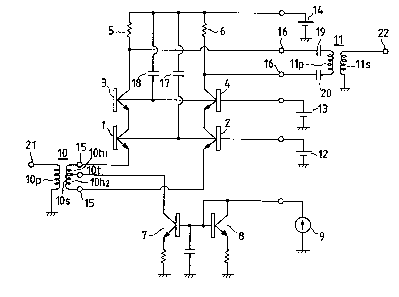
Fig. 1 is a circuit configuration diagram showing
the structure of a first embodiment of a grounded-base
transistor amplifier in accordance with the present
invention;
Fig. 2 is a characteristic diagram showing the noise
figure (NF) in the grounded-base transistor amplifier in
accordance with the embodiment;
Fig. 3 is a circuit configuration diagram showing
the structure of a second embodiment of a grounded-base
transistor amplifier in accordance with the present
invention;
Fig. 4 is a circuit configuration diagram showing
the structure of a third embodiment of a grounded-base
transistor amplifier in accordance with the present
invention;
Fig. 5 is a circuit configuration diagram showing an
example of the structure of an already-known grounded-
11
2158~~~
emitter differential transistor amplifier;
Fig. 6 is a circuit configuration diagram showing a
first example of the structure of a grounded-base
differential transistor amplifier which has been devised
prior to the grounded-base transistor amplifier in
accordance with the present invention; and
Fig. 7 is a circuit configuration diagram showing a
second example of the structure of a grounded-base
differential transistor amplifier which has been devised
prior to the grounded-base transistor amplifier in
accordance with the present invention.
DESCRIPTION OF THE PREFERRED EMBODIMENTS
The embodiments of the present invention will be
described in detail with reference to the accompanying
drawings.
Fig. 1 is the circuit configuration diagram showing
the structure of the first embodiment of the grounded-
base transistor amplifier in accordance with the present
invention.
The grounded-base transistor amplifier illustrated
in Fig. 1 includes a pair of amplifying transistors 1 and
2, a pair of buffer transistors 3 and 4, first and second
collector load resistors 5 and 6, first and second
12
~1~~~~8
transistors 7 and 8 constituting a current mirror circuit
(constant-current circuit), a constant-current source 9,
an input high-frequency transformer 10 connected for
unbalanced-to-balanced conversion, a primary winding 10p,
a secondary winding 10s, a midpoint tap 10t, half
windings lOhl and 10h2, an output high-frequency
transformer 11 connected for balanced-to-unbalanced
conversion, a primary winding 11p, a secondary winding
11s, first and second base bias power supplies 12 and 13,
an operating power supply 14, a signal input terminal 15,
a signal output terminal 16, first and second shunt
capacitors 17 and 18, and first and second coupling
capacitors 19 and 20.
The emitters of the pair of amplifying transistors 1
and 2 are connected to the signal input terminal 15 and
the bases are commonly connected to one end of the first
base bias power supply 12 and to one end of the first
shunt capacitor 17, and the collectors are connected to
the emitters of the pair of buffer transistors 3 and 4.
The bases of the pair of buffer transistors 3 and 4 are
commonly connected to one end of the second base bias
power supply 13 and to one end of the second shunt
capacitor 18. The collector of the transistor 3 is
connected to one end of the first collector load resistor
and to one end of the first coupling capacitor 19. The
13
21~~~~8
collector of the transistor 4 is connected to one end of
the second collector load resistor 6 and to one end of
the second coupling capacitor 20. The pair of
transistors 1 and 2 are constructed by transistors having
relatively large emitters, whereas the pair of buffer
transistors 3 and 4 are constructed by transistors having
relatively small emitters. Commonly connected to the
current mirror circuit are the bases of the first and
second transistors 7 and 8, and connected to the commonly
connected bases are the collector of the second
transistor 8 and one end of the constant-current source
9. In the input high-frequency transformer 10, one end
of the primary winding lOp is connected to an unbalanced
signal input terminal 21 and the other end thereof is
connected to the grounding point. Both ends of the
secondary winding lOs are connected to the signal input
terminal l5, the midpoint tap lOt thereof being connected
to the collector of the first transistor 7 of the current
mirror circuit. In the output high-frequency transformer
11, both ends of the primary winding llp are connected
the other end of the first coupling capacitor 19 and to
the other end of the second coupling capacitor 20; one
end of the secondary winding lls is connected to an
unbalanced signal output terminal 22 and the other end
thereof is connected to the grounding point. The other
14
.'
- 2158~~8
ends of the first and second collector resistors 5 and 6
are connected to one end of the operating power supply
14. The other end of the constant-current source 9, the
other ends of the first and second base bias power
supplies 12 and 13, and the other end of the operating
power supply 14 are all grounded.
The following describes the operation of the
grounded-base transistor amplifier of the first
embodiment which has the structure stated above.
When a constant current is supplied from the
constant-current source 9 to the current mirror circuit,
the value of the current flowing through the second
transistor 8 is set in accordance with the value of the
constant current and the value of the sink current
flowing through the first transistor 7 is also set by the
current mirror function. The sink current flowing
through the first transistor 7 causes the currents
flowing from the operating power supply 14 to the first
collector resistor 5, the collector/emitter path of the
buffer transistor 3, the collector/emitter path of the
amplifying transistor 1, and the half winding lOhl of the
secondary winding lOs and also the currents flowing from
the operating power supply 14 to the second collector
resistor 6, the collector/emitter path of the buffer
transistor 4, the collector/emitter path of the
215868
amplifying transistor 2, and the half winding 10h2 of the
secondary winding 10s, to flow through the midpoint tap
lOt of the secondary winding lOs of the input high-
frequency transformer 10 connected to the collector of
the first transistor 7. This causes the operating bias
current to be applied to the pair of amplifying
transistors 1 and 2 and the pair of transistors 3 and 4.
With such an operating bias current set, when an
unbalanced high-frequency signal is supplied to the
unbalanced signal input terminal 21, the unbalanced high-
frequency signal is converted to a balanced high-
frequency signal through the input high-frequency
transformer 10 before it is supplied to the emitters of
the pair of amplifying transistors 1 and 2 via the signal
input terminal 15. Then, the balanced high-frequency
signal is amplified through the pair of transistors 1 and
2 in the grounded-base mode and led out to the collectors
thereof before it is supplied to the emitters of the
following pair of buffer transistors 3 and 4. The
amplified balanced high-frequency signal is further
amplified through the pair of buffer transistors 3 and 4
in the grounded-base mode and led out to the collectors
thereof and supplied to the high-frequency transformer 11
via the first and second coupling capacitors 19 and 20.
The amplified balanced high-frequency signal is converted
16
2158~~8
back to the unbalanced high-frequency signal through the
high-frequency transformer 11 before it is supplied to
the unbalanced signal output terminal 22.
During such amplification of the high-frequency
signal, the noise voltage generated by the first
transistor 7 of the current mirror circuit is supplied
from the collector of the first transistor 7 to the
midpoint tap lOt of the secondary winding lOs of the
input high-frequency transformer 10; a noise current
based on the noise voltage of the transistor 7 flows
through the two half windings lOhl and 10h2 of the
secondary winding 10s. The noise current flowing through
the two half windings 10h, and 10h2 causes in-phase noise
voltages to appear at both ends of the secondary winding
lOs of the input high-frequency transformer 10 because
the numbers of turns of the two half windings lOhl and
10h2 are the same and the inductance values thereof are
therefore the same. Hence, the noise voltage from the
transistor 7 is applied in the same phase to the emitters
of the pair of transistors 1 and 2. The noise voltage is
amplified through the pair of transistors 1 and 2 and the
buffer transistors 3 and 4 and it reaches the collectors
of the pair of buffer transistors 3 and 4; however, the
noise voltage appearing at the collector of the buffer
transistor 3 is in the same phase as that appearing at
17
21~~6~
the collector of the buffer transistor 4 and therefore
the noise voltage does not appear across the collectors
thereof. Accordingly, when a balanced signal is taken
out through the collectors of the pair of buffer
transistors, the noise voltage is cancelled an it does
not appear in the output. To take out a signal in the
unbalanced mode without causing a noise voltage to appear
at the unbalanced signal output terminal 22, the signal
should be taken out via the output high-frequency
transformer 10 which is connected in the balanced-to-
unbalanced conversion mode as shown in Fig. 1.
In the first embodiment, the emitters of the pair of
transistors 1 and 2 are connected to the collector of the
transistor 7 via the secondary winding lOs of the input
high-frequency transformer 10. In this case, no noise
voltage is produced because no power is consumed at the
secondary winding lOs and no emitter resistor, which
consumes power, is connected to the emitters of the pair
of transistors 1 and 2. For this reason, the NF can. be
decreased in the amplification by the grounded-base
differential transistor of the first embodiment. This
noise controlling effect cannot be obtained by the
grounded-base differential transistor amplifier according
to the first example shown in Fig. 6 or the second
example shown in Fig. 7; only the grounded-base
18
215$68
differential transistor amplifier of the first embodiment
provides the effect.
Referring to the characteristic diagram shown in
Fig. 2, the NF in the grounded-base transistor amplifier
of the first embodiment is indicated by a characteristic
curve a. For the purpose of comparison, the NF in the
grounded-base transistor differential amplifier of the
second example illustrated in Fig. 7 is indicated by a
characteristic curve b.
In Fig. 2, the axis of ordinate indicates the NF and
the axis of abscissa indicates signal source impedance
(Rs). Curve a represents the characteristics of the
grounded-base transistor amplifier of the first
embodiment and curve b represents the characteristics of
the grounded-base transistor differential amplifier of
the second example.
It has been theoretically identified that the NF of
an amplifier generally depends mainly on the signal
source impedance Rs, input impedance (Zin) of an
amplifier, and equivalent noise resistance (Rn) of the
amplifier. The grounded-base transistor amplifier of the
first embodiment should not be directly compared with the
already-known grounded-emitter transistor differential
amplifier illustrated in Fig. 5 or the grounded-base
transistor differential amplifier of the first example
19
21~~5~~
shown in Fig. 6 because they differ in the input
impedance (Zin) of the amplifier, the equivalent noise
resistance (Rn) of the amplifier and other factors.
Nevertheless, the comparison between the grounded-
base transistor amplifier of the first embodiment and the
grounded-base transistor differential amplifier according
to the second example illustrated in Fig. 7 has revealed
the following. As shown in Fig. 2, no significant
improvement in the NF is observed between the grounded-
base transistor amplifier of the first embodiment and the
grounded-base transistor differential amplifier according
to the second example when the signal source impedance
(Rs) is tens of ohms (~2) or less however, the NF in the
grounded-base transistor amplifier of the first
embodiment is dramatically improved over the NF in the
grounded-base transistor differential amplifier according
to the second example when the signal source impedance
(Rs) exceeds tens of ohms (S2) .
As stated previously, the pair of amplifying
transistors 1 and 2 in the first embodiment are
relatively large. According to the general rule of
transistors that the noises in large transistors are
smaller than those in small transistors, the noises in
the amplifying transistors 1 and 2 are small, thus
enabling the amplification with a small NF.
215~62~
On the other hand, the use of the relatively large
amplifying transistors 1 and 2 is accompanied by a
relatively large collector parasitic capacitance composed
primarily of a collector junction capacitance of the
amplifying transistors 1 and 2. Connecting the collector
load resistors 5 and 6 directly to the collectors of the
amplifying transistors which have the large collector
parasitic capacitance would result in a large time
constant which depends on the collector load resistors 5
and 6 and the relatively large collector parasitic
capacitance, making it difficult to achieve the
amplification characteristics with good high frequency
characteristic.
The first embodiment includes the relatively small
buffer transistors 3 and 4 in addition to the amplifying
transistors 1 and 2; the relatively small transistors 3
and 4 provide relatively small collector capacitances
accordingly. This enables a small value of the time
constant which is determined by the collector load
resistors 5 and 6 and the collector parasitic
capacitance. In this case, the collectors of the
amplifying transistors 1 and 2 are coupled to the
emitters of the buffer transistors 3 and 4, generally
leading to a relatively small impedance of the emitters.
This allows the amplification to be implemented with good
21
21562
frequency characteristics.
Thus, according to the first embodiment, the
emitters of the pair of amplifying transistors 1 and 2
receive only the noise signal from the transistor 7 which
constitutes the constant-current circuit and the noise
voltage thereof is cancelled between the collectors of
the amplifying transistors 1 and 2 and it hardly appears
in the output. As a result, the noise can be controlled
to a sufficiently low level and amplification with a good
high frequency characteristic can be implemented.
The first embodiment relates to an example wherein
the pair of buffer transistors 3 and 4 are connected to
the output terminals of the pair of amplifying
transistors 1 and 2. The present invention, however, is
not limited to examples having such configuration; it may
be applied also to a case wherein a pair of relatively
small amplifying transistors are used. Further, when
relatively small collector parasitic capacitances can be
obtained or when the deterioration in frequency
characteristics is allowed to a certain extent or in
other similar cases, the pair of buffer transistors 3 and
4 may be omitted if possible and the collectors of the
pair of amplifying transistors 1 and 2 may be connected
to the collector load resistors 5 and 6.
Furthermore, in the first embodiment, the balanced
22
215~~28
high-frequency signal is converted to the unbalanced
high-frequency signal through the output high-frequency
transformer 11 before it is taken out from the unbalanced
signal output terminal 22. The invention, however, is
not limited to such configuration; it may be applied to a
different configuration wherein the output high-frequency
transformer 11 is omitted and the balanced high-frequency
signal is supplied to the signal output terminal 16 so
that the balanced high-frequency signal may be taken out
through the signal output terminal 16.
In addition, the first embodiment employs the
unbalanced-to-balanced transformer for the input high-
frequency transformer 10 and the balanced-to-unbalanced
transformer for the output high-frequency transformer 11.
The invention, however, is not restricted to such a
configuration; it may also be applied to a different
configuration wherein the balanced-to-unbalanced
transformer is used for the input high-frequency
transformer 10 and/or the output high-frequency
transformer 11.
A resistor of a small resistance value may be
inserted as a kind of a ballast resistor between the
emitters of the pair of grounded-base transistors and the
secondary winding of the input high-frequency transformer
in order to make the current operating point of the pair
23
21~8~28
of grounded-base transistors stable against the
variations in the base/emitter voltage and current
characteristics of the transistors. Such a resistor does
not need to have a large resistance value unlike the
resistors 43 and 44 shown in Fig. 6 which are required to
provide relatively large resistance values. In this
case, however, attention should be paid to the fact that
the noise slightly increases although the noise produced
can be reduced to a lower level because of the smaller
resistance value.
Fig. 3 is the circuit configuration diagram showing
the structure of the second embodiment of the grounded-
base transistor amplifier in accordance with the present
invention. The second embodiment employs the first and
second coils in place of the input high-frequency
transformer 10.
In Fig. 3, reference numeral 23 denotes the first
coil, reference numeral 24 denotes the second coil which
has the same inductance value as the first coil 23, and
reference numeral 25 denotes the node of the first coil
23 and the second coil 24. Other component elements
which are the same as those shown in Fig. 1 are assigned
the same reference numerals.
The second embodiment differs from the first
embodiment only in that it is equipped with the first and
24
second coils 23 and 24, whereas the first embodiment is
equipped with the input high-frequency transformer 10
which includes the secondary winding lOs having the
midpoint tap 10t. There is no other structural
difference between the second embodiment and the first
embodiment; therefore, no further description of the
structure of the second embodiment will be given.
The operation and the advantages of the second
embodiment are almost the same as those of the first
embodiment described above; therefore, no further
description of the operation and advantages will be
given. It should be noted, however, that the second
embodiment provides an additional advantage in that the
grounded-base differential transistor amplifier according
to the second embodiment is available at a lower cost
than the one according to the first embodiment because
the second embodiment does not require the input high-
frequency transformer 10.
A single center tap type coil can replace all the
first coil 23, the second coil 24, and the node 25. When
such a center tape type coil is employed, the
interconnection between the first coil 23 and the second
coil 24 is enhanced. As a result, just like the first
embodiment, the noise from the transistor 7 constituting
the constant-current circuit can be applied to the
2~.5~~~~
emitters of the grounded-base transistors 1 and 2 with
better balance, enabling the noise appearing across the
signal output terminals 16 and 16 to be balanced better.
In other words, a better NF characteristic can be
obtained by using the center tap type coil although the
coil structure is slightly more complicated.
Fig. 4 is the circuit configuration diagram which
shows the structure of the third embodiment of the
grounded-base transistor amplifier according to the
present invention; it shows an example wherein a
capacitor is connected in parallel to the first coil 23
and the second coil 24.
In Fig. 4, reference numeral 26 denotes a capacitor
and reference numeral 27 denotes a parallel resonance
circuit. The other component elements which are the same
as those shown in Fig. 3 are assigned the same reference
numerals.
Structurally, the third embodiment differs from the
second embodiment only in that it is equipped with a
parallel resonance circuit 27 constructed by the first
coil 23 and the second coil 24 which are connected in
series and a capacitor 26 which is connected in parallel
to the above-mentioned coils. There is no other
structural difference between the third embodiment and
the second embodiment; therefore, no further description
26
of the structure of the third embodiment will be given.
The operation and the advantages of the third
embodiment are almost the same as those of the second
embodiment described above; therefore, no further
description of the operation and advantages will be
given. It should be noted, however, that the third
embodiment provides the following additional advantage
which is not available with the second embodiment:
setting the resonance frequency of the parallel resonance
circuit 27 constituted by the first and second coils 23
and 24 and the capacitor 26 so that it is equivalent to
the frequency of the signal applied to the emitters of
the pair of transistors 1 and 2 enables only the signal
component to be applied efficiently to the emitters of
the pair of transistors 1 and 2, thereby attaining higher
amplification efficiency in the pair of transistors 1 and
2.
In this case, a balanced signal may be supplied to
both ends of the parallel resonance circuit 27 or an
unbalanced signal may be supplied to one end of the
parallel resonance circuit 27, the other end thereof
being grounded.
Thus, as described above, according to the present
invention, the noise voltage generated by the transistor
7 constituting the constant-current circuit is applied to
27
the emitters of the pair of transistors 1 and 2 via the
first and second coils 23 and 24, then it is amplified
through the transistors 1 and 2 before it is output from
the collectors thereof. The noise voltages applied to
the emitters, however, bear the in-phase relationship and
the noise voltages output to the respective collectors
also carry the in-phase relationship; therefore, no noise
voltage appears across the collectors of the pair of
transistors 1 and 2. Hence, there is an advantage in
that a grounded-base differential transistor amplifier
with a dramatically decreased NF can be achieved.
Further according to the present invention, since
there is no emitter resistor through which DC currents
flow into the emitters of the pair of transistors 1 and
2, the noise voltage generated by such an emitter
resistor is not applied to the emitters of the pair of
transistors 1 and 2. This aspect also leads to the
advantage in that a grounded-base differential transistor
amplifier with a significantly decreased NF can be
achieved.
In this case, providing the emitters of the pair of
transistors 1 and 2 with the first and second coils 23
and 24 connected in series eliminates the need of the
expensive unbalanced-to-balanced conversion type high-
frequency transformer 10. This provides an additional
28
advantage in that an inexpensive grounded-base transistor
amplifier can be achieved. As another additional
advantage, efficient amplification is ensured by reducing
unnecessary signals so that only a required signal may be
applied to the respective emitters of the pair of
transistors 1 and 2.
29