Note : Les descriptions sont présentées dans la langue officielle dans laquelle elles ont été soumises.
!. ,
WO 95/06270
PCT/US94/09050
1
POLYMER MICROSTRUCTURES WHICH FACILITATE
FIBER OPTIC TO WAVEGUIDE COUPLING
Background of the Invention
~o
1. Field of the Invention
The present invention is directed to an optical coupling device
for facilitating the coupling of an optical fiber to an optical waveguide
and to a method for fabricating such coupling device. Another aspect
of this invention relates to optical fiber to optical waveguide
interconnect comprising the coupling device of this invention, and
arrays comprising, a plurality of such arrays.
2. Description of the Prior Art
2 o Recent developments in the area of optical communications
have provided a large number of optical waveguide devices for the
control and routing of light. Optical waveguide devices which are
created on independent substrates are often referred to as planar
integrated optical devices or photonic devices. These devices can be
2 s further characterized as passive devices, those which serve only to
route the propagation of light along a particular path, and active
devices, those which control some function of the propagating light,
such as its intensity or polarization, or which dynamically control the
path along which the light propagates. However, the propagation of
3 0 light on a substrate bearing an optical waveguide is usually suitable
only for short propagation distances, usually much less than a meter.
For longer distance propagation the optical fiber is the medium of
choice due to its excellent transmission characteristics and ability to
be fabricated in lengths of many kilometers. Therefore, if an optical
35 waveguide device is to be utilized in an optical communication or
WO 95/06270 PCT/US94l09050
2
sensor or distribution system, it is usually required that it be coupled
to an optical fiber at least one point, and often at many points, on the .
substrate. An optical waveguide device which has been coupled to
lengths of optical fibers for ease of insertion into an optical fiber
system is sometimes referred to as a "pigtailed" waveguide device by
1o those skilled in the art. Light propagates through the core region of
optical fibers and these core regions can be as small as a few microns
in diameter. Thus, in order that the fiber to waveguide coupling is
accomplished in an efficient manner that does not waste most of the
light, the alignment of the fiber to the waveguide is of necessity a
critical parameter. Numerous articles and methods have been devised
in the prior art to provide for efficient coupling of optical fibers to
substrates bearing optical waveguide devices. The need for critical
alignment tolerances has resulted in a high degree of complexity and
cost for these devices and methods of the prior art. There are many
2 o descriptions of methods which utilize silicon "V-grooves" as a
positioning element, such as US 4,767,174, which make use of the
fact that certain crystalline orientations of silicon can be preferentially
etched to a high degree of accuracy. This is accomplished by a series
of lithographic steps including resist coating and exposure, followed
by liquid etching. However, the V-groove, once fabricated, serves
only to position the optical fiber relative to the surface of the silicon
wafer. It still remains to position the fiber end relative to the
waveguide end. This is usually accomplished by micromanipulation of
the two components relative to each other followed by fixing the
3o alignment by an optical quality glue. Micromanipulation is an
expensive and time consuming operation for use in a manufacturing '
operation. Alternatively, the V-groove and optical fiber can be
positioned relative to the waveguide by the use of additional
positioning elements, but these also increase the complexity and
therefore cost of the method. Even when the V-groove technique is
WO 95/06270 PCTlUS94/09050
3
utilized only to couple two optical fibers to one another, as in US
4,973,126 there are several additional positioning elements required.
Also, the V-groove techniques serve to position an optical fiber
relative to some surface, such as that of the silicon itself, but the V-
groove does not provide any force to retain the optical fiber in
1o position. That is, the optical fiber can easily slip out of the groove
unless one or more additional elements are present to provide some
retaining force. Typically, a cover plate or a second substrate
containing V-grooves is forced down in contact with the optical fibers
to hold them in the V-grooves and an optical cement or photopolymer
is used to hold the assembly together.
Several methods have been taught in the prior art for creating
optical fiber positioning devices on the substrate which also bears a
waveguide or integrated optical device. These techniques do serve to
reduce the overall number of separate elements which must be
2 o assembled to complete the optical fiber to waveguide coupling.
However, the techniques still remain complex in manufacture or they
lack sufficient retaining force to provide a simple, low-cost, yet
effective method of providing such a coupling. US 5,150,44.0
describes a method wherein waveguides are printed in a plastic film,
in which film are subsequently created rectangular grooves, as by
excimer laser ablation of the film near the waveguide terminus.
Subsequently, the film bearing the waveguide and grooves is
laminated on both sides with additional film layers such that the
openings of square cross section are created in the plane of the
3 o waveguide. The ends of the openings are generally made accessible
and smooth by a subsequent microtoming step. The square opening
is then filled with a liquid photopolymer adhesive and optical fibers are
then admitted into the square opening and fixed in place with a
cementing process. This method involves a large number of
manufacturing steps such as lamination and excimer laser ablation
WO 95/06270 ' PCT/US94/09050
- 4
and is limited to the specific waveguide type of invention, that is, to
waveguides created in thin plastic sheets of the same order thickness
as the waveguide which can be conveniently notched by methods
such as laser ablation. The method does not provide for a convenient
method of attaching optical fibers to optical waveguides created on
l0 other useful substrates such as semiconductor wafers, polyimide
circuit board materials, glass, lithium niobate and other crystalline and
ceramic substrates. Neither does it provide for a method of attaching
optical fibers to any film except those which are the thickness of the
optical waveguide, unless they are supported on another layer which
is removable after the notching process, which adds further
complexity to the manufacturing process. US 4,735,677 describes a
method for providing guides for aligning optical fibers on the surface
of a silicon substrate. In this method it is necessary to first grow a
layer of glass on the silicon wafer by a soot process wherein a glass
precursor is treated by flame hydrolysis to deposit glass particles on
the silicon, followed by heating in an electric furnace to consolidate
the glass. This layer of glass is then lithographically patterned and
etched, as by reactive ion etching (RIE), to form the positioning
elements. After formation of these elements, an optical fiber can be
inserted between them and fixing is accomplished with an adhesive or
by melting the glass with a C02 laser beam. This technique involves
a great number of processing steps and is limited to substrates which
are not damaged by high temperature processes or those which do
not contain sensitive electronic devices which would be damaged by
3 o an RIE etch. A number of desirable substrates for waveguide devices
such as polyimide printed circuit boards and polycarbonate would not
be useful for these reasons. Further, like the V-groove techniques, it
serves only to position the optical fibers yet provides no rigidity or
retaining force to the coupling except through the addition of an
adhesive or another high temperature melting process. Several
SUBSTITUTE SHEET (RULE 26~
WO 95/06270
PCT/US94/09050
5 methods for forming fiber optic positioning devices in molded
thermoplastics are provided. Japan Kokai Patent 278004 provides for
optical fiber guide grooves of approximately triangular cross section
' by a method of compression molding a thermoplastic resin in a die.
This essentially provides a die-molded plastic version of a silicon V-
groove. While eliminating the need for a lithographic etch to produce
the V-grooves, the remaining drawbacks of the technique remain.
Thus the need to align the V-grooves to the waveguide is still present
and the need for additional elements to hold the fiber optics into the
V-grooves still exists and is taught in Kokai Patent 278004. Japan
Patent Publication 254404 further teaches hybrid optical circuits
formed by die-molding an inorganic glass or a plastic resin. The result
is a substrate bearing positioning elements for optical devices and
optical fibers such as with US 4,735,677, but without the need to
deposit a soot layer and etch. However, the shape of the optical fiber
holding channel must be such that the dimension of the top is equal
to or larger than the bottom, or it will be difficult or impossible to
release the substrate from the die mold. Japan Patent Publication
254404 teaches that release from the mold is made easier if the
holding blocks are made V-shape or trapezoid shape with the top of
the channel larger than the bottom of the channel. Thus again, this
method partially solves the problem of positioning an optical fiber
relative to a waveguide, but does not provide for a secure retaining
force on the fiber. In all of these prior art methods, some force must
be applied to hold the optical fiber within the positioning grooves.
3 0 Further, if a liquid optical cement or photoactive monomer or optical
matching fluid is introduced to the coupling region it will wet between
the optical fiber and the wall of the positioning groove by the force of
capillary action. This will serve to float the fiber within the groove
and thus misalign it with the waveguide, unless the secondary
element is present to hold the optical fiber down within the groove
'SUBSTITUTE SHEET (RULE 26)
WO 95106270 PCT/US94/09050
with a greater force. The methods of die molding a plastic resin
suffer the additional drawback of the necessity of maintaining the die
free of any contamination. If the grooves in the master die which will
form the waveguide or the positioning elements become contaminated
on repeated use, the error will be faithfully repeated on each
io successive molding, and prevent accurate optical fiber positioning.
Finally, in the die mold method of Japan Patent Publication No.
254404, the substrate, waveguide and positioning elements are
formed together from the same material. This precludes the ability to
position optical fibers to waveguides created on other desirable
substrates such as silicon wafers, lithium niobate wafers and printed
circuit boards, and limits the choice of waveguide material to the
class of die-moldable plastics and glasses.
Thus, the need remains for devices and methods which allow
for simple, accurate positioning of optical fibers to optical waveguides
on a variety of desirable substrates, which do not require many
additional manufacturing steps or positioning elements or elaborate
alignment by micromanipulator and which provide a secure retaining
force to the optical fiber without the need for additional elements held
in place by optical adhesives or thermal heat treatments.
One aspect of this invention is directed to an optical coupling
device comprising:
a substrate having a surface region at a pre-determined position
on a surface of said substrate for placement of an optical waveguide;
and
a channel on the surface of said substrate for optically aligning
and coupling an optical fiber having a diameter dimension d~ and an
optical waveguide positioned at said predetermined position, wherein
the longitudinal axis of said channel is in alignment with said
WO 95/06270 PCTJUS94/09050
7
predetermined position such that on placement of said optical fiber in
said channel and placement of said optical waveguide in said position
the light carrying core of said fiber and said waveguide are in optical
alignment or substantially in optical alignment, said channel having
sidewalls and a floor wherein the separation of said sidewalls at a
1o cross-sectional depth dimension d2 in the direction normal to said
floor has a width W1 and the separation of said sidewalls adjacent to
said floor has a width W2, wherein W1, W2, d1, and d2 are selected
such that:
(a) W2 is greater than W 1;
(b) d2 is greater than 1 /2 d 1; and
(c) d 1 is greater than W ~ and is equal to or less than W2,
wherein on placement of said optical fiber in said channel the force
required to displace said optical fiber from said channel is equal to or
greater than about 0.01 Newton (N), as determined by the test
2 o method depicted in F1G. 10 and described herein below (hereinafter
referred to as "retaining force test").
Another aspect of this invention is directed to a optical coupling
device with an optical waveguide comprising:
a substrate;
an optically transmissive waveguide on a surface of said
substrate; and
a channel on the surface of said substrate for optically aligning
and coupling an optical fiber having a diameter dimension d 1 and said
optical waveguide, wherein the longitudinal axis of said channel is in
3 o alignment or substantially in alignment with said waveguide such that
on placement of said optical fiber in said channel the light carrying
core of said fiber and said waveguide are in optical alignment or
substantially in optical alignment, said channel having sidewalls and a
floor wherein the separation of said sidewalls at a cross-sectional
depth dimension d2 in the direction normal to said floor has a width
WO 95106270 PCT/~1594/09050
8
W~ and the separation of said sidewalls adjacent to said floor has a
width W2, wherein W 1, W2, d ~ , and d2 are selected such that: ,
(a) WZ is greater than W ~ ;
(b) d2 is greater than 1 /2 d ~ ; and
(c) d ~ is greater than W 1 and is equal to or less than W2,
1o wherein on placement of said optical fiber in said channel the force
required to displace said optical fiber from said channel is equal to or
greater than about 0.01 Newton (N), as determined by retaining force
test.
Still another aspect of this invention relates to an optical fiber
to optical waveguide interconnect comprising:
a substrate;
an optically transmissive waveguide positioned on a surface of
said substrate: and
a channel on the surface of said substrate for optically aligning
2 o and coupling an optical fiber having a diameter dimension d 1 and said
optical waveguide, wherein the longitudinal axis of said channel is in
alignment or substantially in alignment with said waveguide, said
channel having said optical fiber positioned therein such that the
light carrying core of said fiber and said waveguide are in optical
alignment or substantially in optical alignment, said channel having
sidewalls and a floor wherein the separation of said sidewalls at a
cross-sectional depth dimension d2 in the direction normal to said
floor has a width W~ and the separation of said sidewalls adjacent to
said floor has a width W2, wherein W ~ , W2, d ~ , and d2 are selected
3 0 SUCK that:
(a) W2 is greater than W~;
(bD d2 is greater than 1/2 d~; and ,
(c) d ~ is greater than W 1 and is equal to or less than W2,
wherein the force required to displace said optical fiber from said
channel is equal to or greater than about 0.01 Newton (N), as
WO 95/06270
' PCT/US94/09050
9
't
determined by retaining force test.
Yet another aspect of this invention is directed to an improved
pigtailed planar optical device having a plurality of optical waveguide
to optical fiber interconnects on the substrate of this invention and a
packaged planar optical device comprising the improved pigtailed
to planar optical device enclosed in a polymeric package.
Still another aspect of this invention relates to a method for
forming an optical coupling device comprising a substrate having a
surface region at pre-determined position on a surface of said
substrate for placement of an optical waveguide, and a polymeric
optical fiber positioning element for optically aligning and coupling an
optical fiber having a diameter d1 and said optical waveguide
positioned at said predetermined position , said polymeric optical fiber
positioning element comprising a channel having sidewalls, wherein
the longitudinal axis of said channel is in alignment or substantially in
alignment with said pre-determined position, such that on placement
of said optical fiber in said channel and said optical waveguide in said
pre-determined position, said optical fiber and said optical waveguide
are in optical alignment or substantially in optical alignment, said
channel having sidewalls and a floor wherein the separation of said
sidewalls at a cross-sectional depth dimension d2 in the direction
normal to said floor has a width W 1 and the separation of said
sidewalls adjacent to said floor has a width W2, wherein W 1, W2, d 1.
and d2 are selected such that:
(a) W2 is greater than W 1;
3 0 (b) d2 is greater than 1 /2 d 1; and
(c) d 1 is greater than W 1 and is equal to or less than W2,
wherein the force required to displace said optical fiber from said
channel is equal to or greater than about 0.01 Newton (N), as
determined by retaining force test, said process comprising the steps
3 5 of:
SUBSTITUTE SHEET (RULE 2$j
WO 95!06270 PCTlITS94/09050
5 a) placing a layer comprising one or more photopolymerizable
monomers onto a surface of a substrate;
b) exposing said layer to a pattern of actinic radiation to form
an exposed pattern of polymerized monomer having the surface
dimensions of said polymer positioning element and a pattern of
10 unexposed monomer; and
c) developing said layer by removing said unexposed monomer
to form said polymer positioning element on the surface of said
substrate wherein the longitudinal axis of said waveguide isn
alignment or substantially in alignment with said position.
This invention also relates to a method for forming an optical
coupling device with an optical waveguide comprising a substrate, an
optically transmissive waveguide positioned on a surface of said
substrate, and a polymeric optical fiber positioning element for
optically aligning and coupling an optical fiber having a diameter d 1
and said optical waveguide, said polymeric optical fiber positioning
element comprising a channel having sidewalls, wherein the
longitudinal axis of said channel is in alignment or substantially in
alignment with the longitudinal axis of said waveguide, such that on
placement of said optical fiber in said channel said optical fiber and
said optical waveguide are in optical alignment or substantially in
optical alignment, said channel having sidewalls and a floor wherein
the separation of said sidewalls at a cross-sectional depth dimension
d2 in the direction normal to said floor has a width W 1 and the
separation of said sidewalls adjacent to said floor has a width W2,
3 0 wherein W 1, W2, d 1, and d2 are selected such that:
(a) W2 is greater than W 1;
(b) d2 is greater than 1 /2 d 1; and
(c) d 1 is greater than W 1 and is equal to or less than W2,
wherein the force required to displace said optical fiber from said
channel is equal to or greater than about 0.01 Newton (N), as
~S~UBSTITUTE SHEET (RULE 26)
WO 95/06270
PCT/US94/09050
11
determined by retaining force test, said process comprising the steps
of:
a) placing a layer comprising one or more photopolymerizable
monomers onto a surface of a substrate having a waveguide thereon;
b) exposing said layer to a pattern of actinic radiation to form
an exposed pattern of polymerized monomer having the surface
dimensions of said polymer positioning element and a pattern of
unexposed monomer; and
c) developing said layer by removing said unexposed monomer
to form said polymer positioning element on the surface of said
substrate wherein the longitudinal axis of said channel is in alignment
or substantially in alignment with the longitudinal axis of said
waveguide.
Yet another aspect of this invention relates to a method for
forming an optical coupling device with an optical waveguide
2 o comprising a substrate, a polymeric optically transmissive waveguide
positioned on a surface of said substrate, and a polymeric optical fiber
positioning element for optically aligning and coupling an optical fiber
having a diameter d ~ and said optical waveguide, said polymeric
optical fiber positioning element comprising a channel having
sidewalls, wherein the longitudinal axis of said channel is in alignment
or substantially in alignment with the longitudinal axis of said
waveguide, such that on placement of said optical fiber in said
channel said optical fiber and said optical waveguide are in optical
alignment or substantially in optical alignment, said channel having
s o sidewalls and a floor wherein the separation of said sidewalls at a
cross-sectional depth dimension d2 in the direction normal to said
floor has a width W~ and the separation of said sidewalls adjacent to
said floor has a width W2, wherein W ~ , W2, d 1, and d2 are selected
such that:
3 5 (a) WZ is greater than W ~ ;
WO 95/06270 ' PCT/US94I09050
c~~~~
'-,.12
(b) d2 is greater than 1 /2 d 1; and
(c) d 1 is greater than W 1 and is equal to or less than W2,
wherein the force required to displace said optical fiber from said
channel is equal to or greater than about 0.01 Newton (N), as
determined by retaining force test, said process comprising the steps
of:
a) placing a layer comprising one or more photopolymerizable
monomers onto a surface of a substrate;
b) exposing said layer to a pattern of actinic radiation to form
an exposed pattern of polymerized monomer having the surface
dimensions of said polymer positioning element and said waveguide,
and a pattern of unexposed monomer; and
c) developing said layer by removing said unexposed monomer
to form said polymer positioning element on the surface of said
substrate wherein the longitudinal axis of said channel is in alignment
or substantially in alignment with the longitudinal axis of said
waveguide.
This invention exhibits one or more advantages. For example, it
is useful on a wide variety of substrates on which optical waveguides
are desired. It does not involve any high temperature processing
which may deleteriously affect the substrate or optical waveguide. It
utilizes a photolithographic method which combines both high
positioning or alignment accuracy with simplicity of manufacturing
method and low cost. It provides for a firm retaining force on the
optical fiber, thus simplifying the attachment of optical fibers to
3 0 optical waveguides, especially for the important case of attaching
multiple fibers or arrays of optical fibers to a single substrate or
optical waveguide array. It provides for an accurate alignment and ,
firm retention of an optical fiber positioned in a small area on the
optical waveguide substrate, thus allowing for a higher density of
optical interconnects than methods of the prior art which utilize bulky
SL~STI'fUTE SHEET (RULE 2~
WO 95/06270
PCT/US94/09050
13
clips and positioning elements. It provides a unique geometry to the
optical fiber positioning channel which is not provided by prior devices
and methods for fabricating same. Finally, it allows for simple
" assembly of optical fibers to optical waveguides, without the
necessity of complex, expensive positioning devices, which would
adversely affect the cost of manufacture.
Brief Description of the Drawings
The invention will be more fully understood and further
advantages will become apparent when reference is made to the
following detailed description of the invention and the accompanying
drawings in which:
FIG. 1 is a perspective view of a preferred optical coupling
device of this invention.
FIG. 2 is a perspective view of an embodiment of a preferred
optical coupling device and optical waveguide of this invention.
FIG. 3 is perspective view of an embodiment of a preferred
optical fiber to optical waveguide interconnect of this invention.
FIG. 4 is a perspective view of the embodiment of FIG. 3
having an optical buffer layer.
FIG. 5 is a cross-sectional view of a preferred optical fiber to
optical waveguide interconnect of this invention depicted in FIG. 3
along line 5'-5.
FIG. 6 is a cross-sectional view of another preferred optical
fiber to optical waveguide interconnect of this invention having a
3 o trapezoidal shaped or substantially trapezoidal shaped channel having
two optical fibers positioned therein.
FIG. 7 is a perspective view of an array of this invention with
more than one optical coupling devices and optical fiber to optical
waveguide interconnected on the surface of a substrate.
FIG. 8 is a perspective view of another preferred array of this
~tBSTITUTE SHEET ERULE 261
WO 95/06270 PCT/US94/09050
14
invention.
FIG. 9 is a perspective view 'with a cutaway section of a
packaged optical fiber to optical interconnect of the invention similar
to that of FIG. 3, but including a polymeric overcoat.
FIG. 10 shows a device for determining the retaining force of
to the coupling device of this invention.
FIG. 11 illustrates a preferred process for the formation of a
coupling device of the present invention.
FIG. 12 illustrates another preferred process for the formation
of a coupling device of the present invention.
D~~~~:~*ion of the Preferred Embodiments
The preferred embodiments of this invention will be better
understood by those of skill in the art by reference to the above
figures. The preferred embodiments of this invention illustrated in the
figures are not intended to be exhaustive or to limit the invention to
the precise form disclosed. They are chosen to describe or to best
explain the principles of the invention, and its application and practical
use to thereby enable others skilled in the art to best utilize the
invention.
One preferred embodiment of the coupling device of this
invention is depicted in FIG. 1 and is identified by the numeral 10.
Device 10 comprises channel 12 positioned on a surface of substrate
20. Channel 12 can be of any shape or length provided that it has a
certain specific geometric dimensions. Channel 12 can be formed by ,
lithographic techniques using photopolymerizable monomers and the
like. Channel 12 can be a single construction or can be formed from .
a number of parts. In the preferred embodiments of the invention
depicted in FIG.1, channel 12 is formed of lithographic techniques and
is formed by a pair of adjacent positioning elements 14 which form
SUBSfilTUTE SHEET (RULE 26)
WO 95/06270 ~ PCT/US94/09050
5 sidewalls 16 and 18 of channel 12 and a portion of the surface of
substrate 20 which forms floor 24 of channel 12. Channel 12 is
positioned on the surface of substrate 20 such that it's longitudinal
axis is in alignment or substantially in alignment with predetermined
position 22 on the surface of substrate 20.
10 Substrate 20 can be formed of any solid material used in the
formation of substrate for conventional optical waveguide devices.
Desired characteristics of these materials include mechanical and
optical stability at typical operating temperatures of the device.
Preferred materials for use in the fabrication of substrate 20 include
15 printed circuit board material, polymers, quartz, glass, fused silica,
semiconductor wafers and inorganic crystals.
A preferred coupling and optical waveguide device of this
invention is depicted in FIG.2 and is represented by the numeral 26.
Coupling and optical waveguide device 26 comprises polymer
positioning elements 14 defining channel 12 on the surface of
substrate 20. Device 26 also includes channel waveguide 28 at a
predetermined position (which corresponds to position 22 in device
10) on the surface of substrate 20 which is in alignment or
substantially in alignment with the longitudinal axis of channel 12.
A preferred optical fiber to waveguide interconnect of this
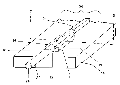
invention is depicted in FIG. 3 represented by the number 30.
Interconnect 30 comprises polymer positioning elements 14, defining
sidewalls 16 and 18 of channel 12, on the surface of substrate 20
and a channel waveguide 28 in alignment or substantially in
3 0 alignment with the longitudinal axis of channel 12. Interconnect 30
also includes optical fiber 32 positioned in channel 12 such that the
light carrying core 34 of optical fiber 32 is in optical alignment or
substantially in optical alignment with waveguide 28 such that light
can be propagated through light carrying core 34 and into optical
channel waveguide 28.
SUBSTITUTE SHEET (RULE 2f~
WO 95/06270 ~ PCT/US94/09050
~~i802~ 16
Another preferred optical fiber to optical waveguide
interconnect of this invention is depicted in FIG. 4 and identified by
the numeral 36. Interconnect 36 includes all of the components of
interconnect 30 identified by like numerals. In addition, interconnect
36 includes optional optical buffer layer 38 on a surface of substrate
l0 20 and waveguide 28 and elements 14 are positioned on the surface
of buffer layer 38. Optical buffer layer 38 is required by the nature of
guided wave propagation of light for those cases where the refractive
index of the substrate is larger than that of the channel optical
waveguide, in order to provide for low propagation loss waveguide
structures. Any material which can provide this function can be used
in the fabrication of buffer layer 38. Illustrative of materials used in
the fabrication of buffer layer 38 are low refractive index
photopolymers, spin-coated polymer layers, spin-on glasses, silicon
dioxide, oxides formed by chemical vapor deposition (CVD) and
fluoropolymers. Preferred materials are low refractive index
photopolymers and fluoropolymers , more preferred materials are low
refractive index photopoiymers.
The relative positions of channel 12 and waveguide 28 or
predetermined position 22 on the surface of substrate 20 is critical to
the invention. As depicted in FIG.s 1, 2, 3 and 4, channel 12 and
waveguide 28 or predetermined position 22 are positioned so that the
longitudinal axis of channel 12 and the longitudinal axis of waveguide
28 or position 22 are in alignment or are substantially in alignment
such that when optical fiber 32 is placed in channel 12 the light
3 0 carrying core 34 of the optical fiber 32 and waveguide 28 or
predetermined position 22 are in optical alignment or substantially in
optical alignment such that light can propagate through core 34 and
into waveguide 28. In the preferred embodiments of the invention as
depicted in the figures, where channel 12 is formed by sidewalls 16
and 18 of elements 14 and floor 24 of substrate 20, elements 14 are
S1)BSTITUTE SHEET (RUL~ 2fi)
WO 95/06270 PCT/US94/09050
17
positioned to provide this effect. In the more preferred embodiment
of this invention where polymer positioning elements 14 are created
by lithographic means from photopolymerizing monomers, elements
14 can be aligned with channel waveguide 28 with a relatively high
degree of accuracy. For example, an especially accurate method of
1o alignment is to create polymeric positioning elements 14 and channel
optical waveguide 28 from the same polymerizable monomers during
the same ultraviolet light (UV) exposure step. This can be
accomplished by placing both lithographic features onto the same
pattern mask or by programming a laser direct-write apparatus to
scan both patterns in a single UV exposure step.
FIG. 5 is a cross-sectional view, along line 5'-5 of FIG. 3, of
interconnect 28 which depicts channel 12, elements 14, sidewalls 16
and 18, optical fiber 32, core 34 and substrate 20 in the requisite
unique geometrical relationships that must exist for the proper
2o functioning of the present invention. The relationship of these
elements is critical to the advantages of this invention. That is,
through use of optical fiber 32 and channel 12 having certain
geometrical parameters on placement of fiber 32 in channel 12 such
fiber 32 is retained in the channel 12 such that the force required to
displace said optical fiber from said channel is equal to or greater than
about 0.01 Newton (N), as determined by retaining force test
depicted in FIG. 10 discussed below. In general, the cross-section of
channel 12 is such that channel 12 has a width dimension of W 1 at a
region of channel 12 at a depth dimension of d2 from floor 24 of
channel 12 in the direction normal to said floor 24 and has a width
dimension of W2 at a region of channel 12 adjacent to floor 24 of
channel 12. Optical fiber 32 has a diameter d 1. To provide the
benefits of this invention, the parameters W 1, W2, d 1, and d2 are
selected such that:
(a) W2 is greater than W 1;
SUBSTITUTE SHEET (RULE 25)
WO 95/06270 , ~ PCT/US94/09050
18
(b) d2 is greater than 1 /2 d 1
(c) d 1 is greater than W 1 and is equal to or less than W2.
The values of W 1, W2, d 1, and d2 may vary widely and still
meet the above conditions, provided that the coupling of optical fiber
32 in channel 12 is such that the force required to displace optical
to fiber 32 from channel 12 is equal to or greater than about 0.01
Newton (N), as determined by retaining force test depicted in F1G. 10
discussed below. However, in general the dominating factors are the
relative values of d1 , d2 and W1 . In the preferred embodiments of
the invention, W 1 is from about 0.6 d 1 to about 0.99 d 1, more
preferably from about 0.8 d 1 to about .99 d 1 and most preferably
from about 0.9 d 1 to about 0.99 d 1. The value of d2 is preferably
from greater than 1 /2 d 1 to about 2 d 1, and is more preferably from
about 0.6 d 1 to about 0.99 d 1 and is most preferably from about 0.8
d1 to about .99 d1. In the embodiments of choice, d2 is from about .
2 0 0.9 d 1 to about 0.99 d 1. The value of d 1 is the diameter of any
optical fiber such as conventional single mode fibers, polarization-
preserving fibers, multi-mode fiber or cable. UV-NIR transmissive fiber
cable and hard polymer clad fiber cable. The value of d 1 is preferably
equal to or less than 1 mm, more preferably from about 125 pm to
about 1 mm and most preferably from about 125 pm to about 250 w
m. In the embodiments of choice the value of d 1 is from about 125 w
m to about 140 pm.
The value of W2 may vary widely and the only requirement is
that W2 is greater than W 1 and is greater than or equal to d 1. W2 is
3 o preferably greater than d 1 to about 2d 1, more preferably from about
1.0 d 1 to about 1.5 d 1 and most preferably from about 1.0 d 1 to
about 1.2 d1. In the embodiments of choice W2 is from about 1.0 d1
to about 1.1 d 1.
The length of channel 12 may vary widely provided that the
force required to displace said optical fiber from said channel is equal
WO 95/06270 PCT/US94109050
19
to or greater than about 0.01 Newton (N), as determined by retaining
force test depicted in FIG. 10 discussed below. In the preferred
embodiments of this invention, the length of channel 12 is equal to or
greater than about d 1. The length of channel 12 is more preferably
from about 0.1 to about 20 mm and is most preferably from about
0.5 to about 10 mm. In the embodiments of choice, the length of
Channel 12 is from about 1 to 5 mm.
The cross sectional shape of channel 12 may vary widely and
still meet the above conditions, provided that the coupling of optical
fiber 32 in channel 12 passes the test of the method of FIG. 10. In
FIG. 5, sidewalls 16 and 18 are depicted as being straight, but this is
not a necessary requirement of the invention, and sidewalls 16 and
18 may be curved, concave, convex or the like, or one may straight
and the other may not, as long as the essential dimensional
requirements of the invention are not violated.
2o In the preferred embodiments of the invention depicted in FIG.s
1 to 5, channel 12 is of trapezoidal or substantially of trapezoidal
cross-section. In the preferred embodiment of FIG. 5, channel 12 is
formed by two parallel or substantially parallel polymer positioning
elements 14 on the surface of substrate 20. Channel 12 has
sidewalls 16 and 18 formed from a side of each of elements 14 and
floor 24 formed by the surface of substrate 20 between elements 14.
As shown in FIG. 5, polymer positioning elements 14 define channel
12 which is of inverted trapezoidal cross section having the longer of
the two parallel or substantially parallel unequal sides with dimension
40 which is greater than dimension 42 of the other of the two
unequal parallel sides, and with the longer of the two parallel unequal
sides of dimension 40 positioned on top and the shorter of the
unequal parallel sides of dimension 42 positioned in contact with the
substrate 20, or the surface of optional buffer layer 38 (See FIG. 4)
s 5 on substrate 20.
WO 95/06270 . PCTIUS94/09050
5 The wall angle which the side of polymer positioning elements
14 makes with the normal to substrate 20 is indicated by the letter a
Angle a must be greater than zero if polymer element 14 is to
possess the preferred shape of an inverted or substantially inverted
trapezoid. If angle a is zero, then the cross section of elements 14 is
1o merely a rectangle as in the prior art and will not possess the
unexpected ability to retain the position of an optical fiber 32 in
channel 12 created between two such elements 14 such that the
coupling passes the test of FIG. 10. The larger that angle a is
fabricated the easier it is to maintain optical fiber 32 within channel
15 12. However, there are practical limitations to how large angle a can
be conveniently fabricated. If angle a becomes too large, then the
width dimension of polymer element 14 (dimension 40 in Fig. 5) must
also become large in order that the base of polymer element 14
(dimension 42 in Fig. 5) has sufficient contact area with substrate 20
2 o to insure relatively good adhesion, and this is deleterious to the
density of interconnections that are a primary benefit of this
invention. Therefore, wall angles a are preferably limited to the range
of from about 1 ~ to about 300. The more preferred range of wall
angles a fall in the range from about 20 to about 250 and most
preferred are wall angles in the range of about 30 to about 20°.
Polymer positioning elements 14 possess certain important
physical properties. These physical properties allow elements 14 to
deform under the applied stress when an optical fiber of diameter d 1
larger than width dimension W1 of the opening at the top of channel
3 0 12 is inserted therein. However, the deformation should not be
permanent and polymer positioning element 14 should as rapidly as
possible return or substantially return to its original dimensional shape
in order to provide for a useful retaining force on optical fiber 32. The
properties must therefore provide some degree of elastic strength.
Also the polymer should not be overly brittle or it will be damaged by
W O 95/06270
PCT/US94/09050
21
the insertion, nor can it be overly hard or it may cause damage to
optical fiber 32. It is clear why the prior art methods utilizing glass
positioning elements are not appropriate from a materials property
standpoint. The polymer preferably is a polymer with a molecular
weight equal to or greater than about 50,000 and more preferably
l0 equal to or greater than 100,000. In the most preferred embodiment
of this invention, the polymer material is a photo-polymer which is a
crosslinked polymer above its gel point, that is, the molecular weight
is essentially infinite. The crosslinked photopolymer not only has the
most preferred physical properties, but is also the simplest case for
removal of the unirradiated monomer as the crosslinked photopolymer
will no longer dissolve in the developing solvent when elements 14
are formed by lithographic techniques. The polymer should be
largely amorphous (less than 50% crystallinity) rather than crystalline
and its glass transition temperature (Tg) should be less than its use
temperature in order to ensure that there is a high degree of chain
segment mobility. It is preferred that the crystallinity of the polymer
is less than about 25°~ and more preferred that the crystallinity is
less than about 10%. In the most preferred embodiment the polymer
is completely amorphous, that is, the crystallinity is about 0%. A
completely amorphous polymer is especially preferred for the
embodiment of the present invention wherein a single lithographic
step is utilized to produce both polymer positioning elements 14 as
welt as polymeric optical waveguide 28 from a single layer of
reactive monomer on a substrate 20, in that it will yield an optical
3 o waveguide with the lowest amount of loss due to scattering of light
from polymer crystalline regions. As to the Tg, since a useful
temperature at which to attach optical fibers to optical waveguide
devices is room temperature, it is essential that the Tg of the
photopolymer is less than room temperature. Thus, it is preferred
that the Tg is less than about 30°C and more preferred less than
SUBSTITUTE SH~ET (RULE 26)
WO 95/06270 PCT/US94/09050
22
1.
about 20°C and most preferred are photopolymer materials whose Tg
is less than 10°C. It is preferred that the Tg of the photopolymer as
just described be an inherent property of the polymer. However, it is
recognized that it is possible to adjust the Tg of a polymer by a
number of methods known in the general art of polymer science, such
as by the addition of plasticizers or by swelling the polymer with a
solvent, and polymers so treated may also be useful in the method of
the invention without departing from its scope. In addition, it is
further recognized that unreacted monomer which is trapped within
the photopolymer matrix may serve as such a plasticizer material.
Further, it is recognized that once the optical fiber is inserted into the
channel structure of the invention, it is no longer required that the Tg
of the polymer positioning elements fall within the critical range.
Such Tg may, at a later time, be adjusted to a higher value as by
evaporation of solvent or plasticizer or as by further cross-linking of
2 0 the polymer. Likewise, though less convenient, a polymer having a
Tg greater than room temperature, i.e. above about 30°C, may be
employed if the assembly of the device is carried out at elevated
temperatures equal to or greater than the Tg of the polymer followed
by cooling to a temperature less than the Tg. The polymer which
makes up positioning element 14 preferably contains a number of
crosslinks to prevent overall movement of the polymer chains and
thus restore the necessary geometry of element 14 after the
introduction of optical fiber 32 into positioning channel 12 between
elements 14. This recovery of the shape of polymer element 14 is
associated with the properties of resilience and low permanent set. In
the preferred case, wherein the polymer material which comprises
positioning element 14 is a crosslinked polymer above its gel point,
there is, of necessity, a minimum of one primary chemical bond
crosslink per polymer chain. In the more preferred compositions at
least one of the reactive monomers is a multifunctional monomer, that
SUBSTITUTE SHEET (RULE 26)
wo 9s/o6z~o
PCT/US94/09050
23
is, it contains two or more reactive functionalities on the same
molecule. When such a multifunctional monomer is present as a
major component of the monomer mixture then the resulting polymer
will be much more extensively crossiinked and there will be many
crosslinks per polymer chain.
The tensile strengths which are displayed by polymers useful in
the invention preferably range from about 100 to about 850 kg cm-2
with the more preferred range being from about 150 to about 300 kg
cm-2 .
The percent elongation of the crosslinked photopolymers useful
in the method of the invention preferably ranges from about 2 to
about 300°~ with the more preferred range being about 2 to about
10096 due to the increased level of crosslinking in the more preferred
compositions. Useful values of hardness preferably range from about
to about 200 s (pendulum hardness) with more preferred values
2 o being about 40 to about 150 s.
A wide variety of polymers can be used in the fabrication of
elements 14. Preferred for use in the fabrication of elements 14 are
photopolymers formed by the photo-polymerization of a
photoreactive monomer or mixtures of such monomers such as
urethane acrylates and methacrylates, ester acrylates and
methacrylates, epoxy acrylates and methacrylates, polyethylene
glycol acrylates and methacrylates and vinyl containing organic
monomers. Illustrative of such acrytate and methacrylate monomers
are aryl diacrylates or methacrylates, triacrylates or rnethacrylates and
3 o tetra acrylates or methacrylates as for example mono-di,-tri- and
tetraacryiates or methacrylates of benzene, naphthalene, bisphenol-A,
biphenylene, methane biphenylene, di-(trifluoromethyl) methane
biphenylene, phenoxyphenylene and the like. Useful monomers also
include aliphatic acrytaies, diacrylates, triacrylates and tetraacrylates
as for example, butyl acrylate, ethylhexyl acrylate, phenoxyethyl
WO 95/06270 PCTIUS94/09050
24
acrylate, p-carboxylethyl acrylate, isobornyl acrylate,
tetrahydrofurfuryl acrylate, cyclohexyl acrylate, propylene glycol
monoacrylate, 2-(2-ethoxyethoxy) ethyl acrylate, N-vinyl
pyrrolidone,l,6-hexanediol diacrylate or dimethacrylate, neopentyl
glycol diacryiate, diethylene glycol diacrylate or dimethacrylate,
1o triethylene glycol diacrylate or dimethacrylate, tetraethylene glycol
diacrylate or dimethacrylate , polyethylene glycol diacrylate or
dimethacrylate, dipropylene glycol diacrylate, tripropyiene glycol
diacrylate, ethoxylated neopentyl glycol diacrylate, propoxylated
neopentyl glycol diacrylate , aliphatic diacrylate, alkoxylated aliphatic
diacrylate, aliphatic carbonate diacryiate, trimethylolpropane
triacrylate or trimethacrylate. pentaerythritol triacrylate, ethoxylated
trimethylolpropane triacrylate, propoxylated trimethylolpropane
triacrylate, glyceryl proxytated triacrylate, tris (2-hydroxyethyl)
isocyanurate triacrylate, pentaerythritol tetraacrylate, dipentaerythritol
2 o pentaacrylate , ditrimethylolpropane tetraacrylate, alkoxylated
tetraacrylate. The most preferred monomers include
trimethylolpropane triacrylate, pentaerythritol triacrylate, ethoxylated
trimethylolpropane triacrylate, glyceryl proxylated triacrylate,
pentaerythritol tetraacrylate, dipentaerythritol pentaacrylate,
ditrimethylolpropane tetraacrylate, methyl methacrylate, n-butyl
acrylate, 2-ethylhexyl acrylate, isodecyl acyiate, 2-hydroxyethyl
acrylate, 2-hydroxypropyl acrylate, cyclohexyf acrylate, 1,4-
butanediol diacrylate, ethoxylated bisphenol A diacrylate,
neopentylglycol diacrylate, diethyleneglycol diacrylate, diethylene
3 o glycol dimethacrylate, 1,6-hexanediol diacrylate, and pentaerythritol
tetra-acrylate.
Especially useful are mixtures wherein at least one monomer is
a multifunctional monomer such as a diacrylate or triacrylate, as these
will produce a network of crosslinks within the reacted photopolymer.
The preferred monomer mixtures for use in the method of the
WO 95/06270 PCT/US94/09050
5 invention are mixture of 33% Genomer T1600 urethane acryiate and
67% 1,6-hexanediol diacrylate; and the mixture of 67% ethoxylated
bisphenol A diacrylate and 33% trimethylol propane triacrylate.
Channel 12 may include a single optical fiber 32 or more than
one optical fiber 32 as depicted in FIG. 6. Turning now to Fig. 6,
1o which is a cross sectional view through the region of the polymeric
positioning elements 14 on a suitable substrate 20. In the following
embodiment, elements 14 are positioned such that two optical fibers
32 are accommodated in the channel 12 which is formed between
elements 14 such that the light carrying core 34 of each optical fiber
15 32 is in optical alignment or substantially in optical alignment with a
waveguide /not depicted) . This also is an embodiment of the present
invention whereby the density of optical waveguides can be increased
or the length and area of the fan-in and fan-out regions can be
reduced. The retaining force on optical fibers 32 is not as great as
2 o the embodiment where only a single optical fiber occupies a
positioning channel, yet it is still sufficient to allow for increased
utility in attaching optical fibers to optical waveguides on substrates
over the methods of the prior art.
A preferred array of this invention is shown in FIG. 7 and is
25 represented by numeral 46. Turning now to Fig. 7, in the following
embodiment, an array of optical waveguides 48 on a single substrate
50 is provided with an aligned array of the polymeric positioning
elements 52 of the present invention. Each pair of elements 52 is
centered on, and parallel to, the centerline of the end of optical
3 o waveguide 48 with which it is associated, the alignment preferably
being accomplished by known methods of the art as for example by
lithography, such as by utilizing exposure masks which also contain
registration marks thereon. The end of optical fiber 54 is shown to be
inserted into one of the channels 56 formed by polymer positioning
3 5 elements 52 such that it light carrying core 58 of fiber 54 is aligned
WO 9SI06270 PC~YUS94/09050
26
and centered on the end of optical waveguide 48. Optical fiber 54 is
f
held firmly in the channel by the retaining force exerted upon it by the
polymer positioning elements which have the required geometry as in
FIG.s 1 to 5, without the necessity of additional elements or optical
glues or melting. This firm positioning allows additional optical fibers
54 to be placed in nearby channels 56 without disturbing the
positioning of optical fiber 54 which is already in place. This .provides
for a greatly increased ease of fabrication for attaching optical fibers
54 to optical waveguides 48 over the methods of the prior art. Also
provided is the ability to introduce each optical fiber in an array
individually, thus overcoming the cumulative positioning error
associated with prior art methods wherein the entire optical fiber array
is loaded simultaneously.
Another preferred array of this invention is depicted in FIG. 8
and is represented by the numeral 60. Turning now to Fig. 8, in
2 o embodiment 60 depicted therein an array of optical waveguides 62 on
a single substrate 64 with an optional optical buffer layer 66 is
provided with an aligned array of polymeric positioning elements 68
such that the positioning elements 68 which are not the outermost
form the sidewall of two adjacent channels 70. That is, the central
polymer positioning elements 68 are shared by two optical
waveguides 62. Thus, if the number of optical fibers 72 to be
attached is n, then the number of required polymer positioning
elements 68 is n + 1. In this manner it is possible to reduce the
separation between adjacent optical waveguides 62 on substrate 64
s o and thereby either increase the density of optical waveguides 62 or
reduce the size of the fan-in and fan-out region of a multi-port optical
waveguide device known to those skilled in the art.
An optical fiber to waveguide interconnect of this invention or
an array of such interconnects as depicted in FIG.s 1 to 8 can be
3 5 fabricated with an overcoat layer as depicted in FIG. 9. Turning now
WO 95/06270 PCT/US94/09050
to Fig. 9, which is a perspective view with a cutaway section through
the region of polymeric positioning elements 52, of the embodiment,
similar to that of FIG. 7. Polymer positioning elements 52 are
lithographically formed by a photopolymerization process on the
surface of substrate 50 which may optionally also bear an optical
io buffer layer (not showy so as to provide a channel structure 56 of
the required geometry. Channel 56 provides both alignment
positioning and retaining force to optical fiber 54 such that the light
carrying core 58 of the optical fiber 54 is held in contact with the end
of optical channel waveguide 48 on the surface of substrate 50.
Polymer positioning elements 52 serve to hold optical fiber 54 in
position while an overcoat material layer 74 is applied to the
structure. Layer 74 serves to protect the optical waveguide structure
from physical damage or dust and also serves as a means of adjusting
the numerical aperture (N.A.) of channel optical waveguide 48 so as
2 o to match the numerical aperture of optical fiber 54 and thereby
reduce the optical losses due to numerical aperture mismatch. Such
an overcoat layer 74 may comprise an optical cement, a reactive
monomer mixture which is cured to a polymer as by thermal or photo
polymerization, a glass precursor which is cured to a glass, or a
plastic or glaaa which is applied by a solution technique followed by
drying. Polymer positioning elements 52 of the present invention
maintain the positioning of optical fiber 54 by the retaining force
imposed by the unique geometry of elements 52 such that optical
fiber 54 is not displaced during the overcoating process, thus
3 0 overcoming the drawbacks of the prior art methods.. Specifically,
optical fiber 54 is not "floated" in channel 56 by the force of capillary
action of the overcoating liquid, but is held down in contact with
substrate 50 by the retaining force generated by the unique geometry
of elements 52. The methods of the prior art require additional
s 5 elements to apply the force necessary to maintain the position of the
WO 95/06270 PCT/US94/09050
c
28
optical fibers during such an overcoating process.
Fig. 10 depicts a test method which illustrates the retaining
force polymer positioning elements 14 provide upon optical fibers
which are inserted therein and for evaluating such force. In the
preferred embodiments of the test depicted in FIG. 10, an array of
io polymer positioning elements 76 and polymer optical waveguides 78
are printed by a process of mask irradiation of a reactive monomer
mixture onto the surface of a silicon wafer substrate 80 bearing a thin
layer of an optical buffer 82. Glass optical fiber 84 is inserted into
one of the channels 86 formed by a pair of polymer positioning
i5 elements 76 such that it is held in alignment with optical waveguide
78. No glues or additional elements are present to increase the
retaining force on optical fiber 84, which is held in place solely by the
retaining force of polymer positioning elements 76. The other end of
optical fiber 84 is inserted into a hole 88 which is drilled into the end
20 of an aluminum block 90, which has a mass of 1 grams, preferably 10
grams, even more preferably 50 grams, more preferably 75 grams
and most preferably 100 grams, and is secured in the hole 88 by
several drops of epoxy glue 92. A block having a mass of 1 gram will
exert a force of 0.01 Newton on the coupling of optical fiber 84 and
25 elements 78 , a block having a mass of 10 grams will exert a force of
0.1 Newton on the coupling of optical fiber 84 and elements 76, a
block having a mass of 50 grams will exert a force of 0.5 Newton on
the coupling of optical fiber 84 and elements 76, a block having a
mass of 75 grams will exert a force of 0.75 Newton on the coupling
3 0 of optical fiber 84 and elements 76, and a block having a mass of
100 grams will exert a force of 1.0 Newton on the coupling of optical
fiber 84 and elements 76. The silicon wafer substrate 80 is placed in
clamp 94 and suspended such that the aluminum block is lifted clear
of the table top 96. Block 90 is allowed to hang from wafer 80, held
3 5 solely by the retaining force generated by the interaction of polymer
WO 95!06270 PCT/LTS94/09050
29
positioning elements 76 (preferably about 5 mm long) with optical
fiber 84 for a period of one hour without any noticeable change in the
position of optical fiber 84 relative to optical waveguide 78. This
method demonstrates the unexpected stability of optical fiber 84 to
optical waveguide 78 coupling which is provided by the channel of
1o this invention having unique geometry which the methods of the prior
art do not provide unless additional elements or cements are present.
Figs. 11 and 12 illustrate the method of the present invention
by which polymer positioning elements of the required unique
geometry are provided. In Fig. 11 is detailed a method whereby
polymer elements 98 are provided by a pattern of mask irradiation
with UV light. Substrate 100 which may optionally be coated with a
layer of optical buffer material 102 is coated with layer of
photoreactive monomer layer 104 to a thickness which is greater than
the radius t h d1) of the optical fiber which is to be coupled to the
optical waveguide. Image mask 106 bearing a pattern of opaque
areas 108 which allow UV light 110 to pass through only in the areas
which comprise the pattern of polymer positioning elements 112, and
optionally the pattern of channel waveguide elements (not depicted),
is positioned above monomer layer 104 in close proximity, and UV
light 110 as for example from a mercury or xenon lamp, is directed to
fall on the surface of image mask 106. UV light 110 which passes
through the clear areas of mask 106 causes a photopolymerization
reaction in the regions 112 of monomer layer 104 which are directly
under those image areas. No photoreaction occurs in those areas of
3 o monomer layer 104 which are shielded from the UV light by the
opaque areas 108 of image mask 106. After irradiation by UV light,
image mask 106 is removed and the unreacted monomer is washed
away with a suitable solvent such as acetone or methanol, leaving a
pattern of photopolymerized structures on substrate 100 which
correspond to polymer positioning elements 98 of the present
WO 95/06270 PCTIUS94/09050
~1~~02~
. 30
invention which define channels 114 having the preferred trapezoidal
or substantially trapezoidal cross section having the required geometry
to pass the test of FIG. 10. The simplicity and ease of
photodelineation of polymer structures and the great alignment
accuracy which is possible with lithographic methods in general,
to allows the method of the present invention to overcome many of the
drawbacks of the methods of the prior art. The unique geometry of
polymer positioning elements 98, that being an inverted trapezoid as
shown on the right hand side of Fig. 11, is achieved by the choice of
proper conditions of irradiation. The optical absorption of the
unreacted monomer layer 104 at the wavelengths of the UV light
must be high enough, such that a gradient of UV light intensity is
established through the film. That is, the amount of UV light available
in the monomer layer to cause the initiation of the photoreaction will
decrease from the top, or the image mask side, towards the bottom,
or the substrate side, due to the finite absorption of the monomer
layer. This gradient of UV light causes a gradient in the amount of
photopolymerization reaction that occurs from top to bottom, and this
results in the unique geometry of the developed polymer structure, a
geometry which is easily accessible with the method of the present
invention, but not easily attained with the methods of the prior art.
The gradient in the amount of photopolymerization which occurs from
the top to the bottom of the film may be further influenced by the
presence of dissolved oxygen gas in the monomer layer, such oxygen
acting to curtail or quench the photopolymerization reaction except in
3 o those areas where ail oxygen has been consumed by the free radicals
produced in the photopolymerization process. Such action of
dissolved oxygen gas on the progress of photopolymerization
reactions is well known to those skilled in the art. Further, the
requisite geometry of the photopolymer structures may be further
influenced by the process of self-focusing. That is, the light falling on
WO 95!06270 PCT/US94/09050
31
the surface of the monomer layer 104 initiates photopolymerization at
that surface, and since the refractive index of the solidified polymer
material is higher than that of the liquid monomer, it acts to refract
the light passing through it. In this manner the aerial image of light
falling on the monomer nearer to the substrate side of the monomer
layer is altered through refraction caused by the already-polymerized
material which lies above it. This effect may cause a narrowing of
the resultant polymerized structure from the top surface, upon which
the imaging light was directed, towards the bottom, or substrate side
of the layer.
In Fig. 12, a UV laser beam 116 is focused onto the surface of
the monomer layer 118 with a focusing optical element 120, such as
a quartz microscope objective, and the photopolyrnerized sections
121 are provided by scanning the focused laser spot on the surface of
monomer layer 118 in a pattern corresponding to the polymer
2 o positioning elements 122, and optionally in the pattern of an optical
waveguide device toot depicted). After the exposure is complete, the
unexposed monomers are rinsed from substrate 124 by a suitable
solvent such as acetone or methanol to yield polymer positioning
elements 122 having the desired geometry on the surface of substrate
124, which may optionally carry a layer of optical buffer 126. In the
case of the method of Fig. 12, the required unique geometry of
polymer positioning elements 122 is provided by the same process of
optical gradient within monomer layer 118, but is also further
enhanced by the focal properties of focusing optical element 120,
3 o which converts the parallel beam of the laser into a focused cone of
light which intersects the monomer layer with a cross section that has
the desired inverted trapezoid geometry. The influences of dissolved
oxygen and self-focusing on the resulting geometry of the fabricated
photopolymer elements may also be considerable in the case of
scanning laser exposure.
WO 95/06270 PCTlUS94/09050
32
Photoreactive monomer layers 104 and 118 comprise a
photopolymerizable monomer or a mixture of such monomers and one
or more photoinitiators and optionally one or more stabilizers. Useful
monomers include those described above for use in the formation of
positioning elements such as methyl methacrylate, n-butyl acrylate, 2-
1o ethylhexyl acrylate, isodecyl acylate, 2-hydroxyethyl acrylate, 2-
hydroxypropyl acrylate, cyclohexyl acrylate, 1,4-butanediol diacrylate,
ethoxylated bisphenol A diacrylate, neopentylglycol diacrylate,
diethyleneglycol diacrylate, diethylene glycol dimethacrylate, 1,6-
hexanediol diacrylate, trimethylolpropane triacrylate, pentaerythritol
triacrylate and pentaerythritol tetra-acrylate and mixture thereof.
Especially useful are mixtures wherein at least one monomer is a
multifunctional monomer such as a diacrylate or triacrylate, as these
will produce a network of crosslinks within the reacted photopolymer,
such as a mixture of Genomer T1600 urethane acrylate and 1,6-
hexanediol diacrylate or a mixture of ethoxylated bisphenol A
diacrylate and trimethylolpropane triacrylate.
A wide variety of photoinitiators are suitable for use in initiating
polymerization by UV light in the monomer mixtures. Many good
descriptions of useful initiators for photopolymer systems are available
in the art including Photopolymerization of Surface Coatings, chapter
3 (1982) by C.G. Roffey. Preferred photoinitiators are those which
are soluble in the preferred monomers and which have useful
absorption at the wavelengths of light chosen for irradiation. If the
necessary unique geometry of the photopolymer element is to be
provided by the establishment of a gradient of photoinitiation events
through the thickness of the monomer layer, then it is important that
the layer has significant optical absorption at the irradiating
wavelength. If the optical absorption of the constituent monomers is
small at these wavelengths the requisite absorption may be provided
by the photoinitiator. Combinations of several photoinitators are
SUBSTITUTE SHEET (RULE 26)
WO 95/06270 PCT/US94/09050
33
useful to broaden wavelength sensitivity or to increase loading
solubility or to match the photospeed of the monomer system to the
particular light source to be employed. Especially useful
photoinitiators in the method of the invention include 2-hydroxy-2-
methyl-1-phenyl-propan-1-one fDarocur 1173), 2,2-dimethoxy-2-
lo phenylacetophenone (Irgacure 651 ) and 1-hydroxycyclohexyl phenyl
ketone sensitized 1:1 with benzophenone (Irgacure 500). An
especially preferred mixture of photoinitiators is a 1:1:1 mixture of
these three sensitizers.
The amount of initiator which is useful in the photomonomer
i5 mixtures is dependent on the desired photo speed at the available
optical power present in the source of irradiation and on the desired
wall angle and thickness of the polymeric positioning element. In
general, less initiator is required for a high brightness, focused source
such as a scanned laser beam and more is required for a low
2 o brightness source such as a mercury lamp which has been spread out
to cover a large area such as a printed circuit board. Useful loadings
of photoinitiators, by percent weight of the total monomer mixture
layer, are 0.1 to 10% with a preferred range of 0.5 to 8% and a most
preferred range of 2 to 6%.
25 The following examples are intended to further teach the utility
of the invention. The scope of the invention is not limited by the
examples. sa other uses within the scope of the invention will be
evident to those skilled in the art. The invention is limited only by the
appended claims.
A silicon wafer was spin coated at 6000 rpm with a
photocurable fluoromonomer mixture [80 parts F8 perfluoropolyether
diol diacrylate, 108 parts F4.0 perffuoropolyether diol diacrylate, 6
parts hexafluoroisobutyfene/ vinyl alcohol copolymer, 3 parts Irgacure
WD 95/06270 PCT/US94/09050
34
500 and 3 parts Darocure 1173] which was then cured under a 1000
Watt xenon lamp for 1 minute under a nitrogen atmosphere to provide
a 4 micron thick optical buffer layer. The wafer was baked for 10
minutes at 120 C, followed by a 30 second oxygen reactive ion etch
(RIE) to improve adhesion of the subsequent waveguide layer. The
io substrate was spread with a 180 micron thick layer of photocurable
acrylate monomer mixture f50 parts Genomer T1600 urethane
acrylate, 98 parts 1,6-hexanediol diacrylate, 1 part Darocure 1173, 1
part Irgacure 651 and 1 part Irgacure 500]. The substrate was placed
on a computer controlled positioning stage under the focused beam of
a UV argon laser. The computer was programmed to move the
sample under the laser beam so as to expose only discrete areas of
the sample in the design of a 3 X 1 channel waveguide combiner,
with individual pairs of polymer positioning elements at the end of
each of the 4 ports of the waveguide device. After the selective
2 o pattern exposure was complete, the substrate was rinsed in acetone
to wash away the unreacted monomer from all areas not exposed to
the laser irradiation. The result was a rib waveguide 3 X 1 combiner
on a semiconductor substrate with precisely aligned polymer
positioning elements to facilitate the attachment of fiber optic
"pigtails". The polymer positioning elements were delineated so that
a bare glass fiber of diameter 140 micron would be tightly held in the
channel formed between them.
3 o The waveguide device of Example 1 was placed under a
dissection microscope to magnify the waveguide termination area.
Bare glass optical fiber strands were hand-inserted into the channels
formed by the polymer positioning elements. It was immediately
noted that, once inserted, the glass optical fibers were held very
3 5 tightly by the polymeric positioning elements. It was therefore quite
wo 95/0620
PCT/US94/09050
5 easy to successively pigtail each of the four waveguide ports without
disturbing any of the previously inserted optical fibers.
The pigtailed device of Example 2 was clamped down under a
1o CCD camera so that the fiber termination area could be observed on a
TV screen. The optical fiber pigtail was held by an XYZ positioning
stage so that it could be moved relative to the waveguide substrate.
The positioning stage was used to translate the optical fiber in both
the in-plane and out-of-plane directions. It was possible to cause a
15 large bend in the optical fiber in either direction without inducing the
optical fiber to come out of the polymer positioning elements.
A pigtailed sample was prepared as in Examples 1 and 2,
2 o except in this case the non-fluorinated acrylate monomer mixture of
Example 1 was utilized to form the optical buffer layer and a higher
index acrylated monomer mixture [96 parts ethoxyiated bisphenol A
diacrylate, 33 parts trimethylolpropane triacrylate, 3 parts Irganox
1010 antioxidant, 1 part Darocure 1173, 1 part Irgacure 651 and 1
25 part Irgacure 5001 was used to form the optical waveguides and the
polymer positioning elements. No reactive ion etching was used.
After the glass optical fiber pigtails were in place, the entire structure
was overcoated with a thick layer of the lower index acrylate
monomer mixture, which was then UV exposed to polymerize it. The
3 o result was a device which was fully encapsulated by a polymer layer
to protect it from dirt and physical damage. The polymer positioning
elements were capable of maintaining the alignment of the glass
optical fibers to the ends of the optical waveguide device during the
overcoating process .without the need for additional retaining
3 5 elements.
WO 95/06270 PCTIUS94/09050
36
_ ~ . ,
EXAMPLE 5
A 3 X 1 combiner was produced as in Example 4 except that
the substrate was polyimide laminate circuit board material rather than
a silicon wafer.
,~1CAMPLE 6
A chrome on glass photomask was produced which contained a
pattern of straight line optical waveguides with sets of polymer
positioning elements of length 5mm at each end. The mask was
brought into contact with a 125 micron thick layer of the high index
photocurable monomer mixture of example 4 on a silicon substrate
bearing a thin layer of the photocured low index optical buffer of
example 4. The sandwich structure of substrate, photocurable
monomer and image mask was placed under the collimated output of
2o a 1000 Watt xenon lamp fitted with UV reflecting optics. The
monomer was exposed for 12 seconds, after which the mask was
removed and the unexposed regions were rinsed away with acetone.
The straight optical waveguides and polymer positioning elements
remained on the optically buffered silicon substrate. A length of glass
optical fiber was inserted into the channel formed by one pair of the
polymer positioning elements so that it was aligned with the polymer
waveguide. The other end of the optical fiber was epoxied to an
aluminum weight weighing 110 grams. After the epoxy dried, the
wafer bearing the waveguide was hung vertically so that the weight
3 o was suspended solely by the gripping action of the polymer
positioning elements. The interaction length between the optical fiber
and the polymer positioning elements was only 5mm and no type of
glue or epoxy was present in this region. The weight was allowed to
hang from the waveguide substrate for several months and no
displacement of the optical fiber occurred.
WO 95/06270 PCT/US94/09050
37
EXAMPLE 7
An optical waveguide with pairs of polymer positioning
' elements at each end was prepared with an image mask exposure as
in Example 6, except that the substrate was a polyimide laminate
1o circuit board material rather than a silicon wafer.
FXAMPLE 8
Example 4 was repeated except that two polymer optical
waveguides were written with a 40 micron separation and the
polymer positioning elements were laser written with a separation
slightly less than twice the diameter of the glass optical fiber. Two
bare optical fiber pigtails were placed in the channel between the
polymer positioning elements at each end of the optical waveguides,
for a total of four pigtails. The polymer positioning elements were
2 o capable of maintaining the alignment of each of the optical fibers to
its respective waveguide during the overcoating process.
Polymer positioning elements were prepared on silicon
substrates by both the focused laser writing process of example 1
and the masked irradiation process of example 6. The crystalline
silicon wafers were then cleave fractured perpendicular to the
polymer positioning elements so as to provide a cross section of the
elements. The cross-sections of the cleaved polymer positioning
3 o elements were then examined by optical and scanning electron
microscopy. The structure of the polymer elements was observed to
have the requisite geometrical shape of a preferred embodiment of the
present invention, that being inverted trapezoids with the longer of
the two unequal parallel sides located on top and the shorter of the
unequal parallel sides located adjacent to the silicon wafer substrate.
WO 95/06270 PCT/US94/09050
38
The resulting shape of the channel between two such structures in
proximity was also of the required geometry of the present invention, _
that being a channel with a smaller opening at the top and a larger
separation at the substrate. The shape of the channel could also be
described as a trapezoid with the longer of its two parallel unequal
1o sides adjacent to the substrate. The width of the channel separation
at the top was less than the 140 micron diameter of a suitable glass
optical fiber, while the bottom separation dimension was adequate to
accommodate such an optical fiber dimension.
EXAMPLE 10
A substrate comprising a sheet of Lexan polycarbonate was
spin coated with a thin layer of the optical buffer material of Example
4 and exposed to a xenon lamp for 10 seconds to cure. The
substrate was then coated with a 20 micron thick layer of a reactive
2 o monomer mixture comprising [56 parts ethoxylated bisphenol A
diacrylate, 19 parts trimethylol propane triacrylate, 21 parts Genomer
T1600 urethane acrylate, 41 parts 1,6-hexanediol diacrylate, 1.7
parts Irganox 1010 antioxidant. 1 part Darocure 1173, 1 part Irgacure
651, 1 part Irgacure 5001. The focused UV laser apparatus of
Example 1 waa used to write a pattern consisting of a rectangular
plateau which was then developed by rinsing with methanol. The
substrate bearing the plateau structure was then coated with a 120
micron thick layer of the high index monomer mixture of Example 4
and the same focused UV laser apparatus was used to write a pattern
3 o corresponding to a straight channel waveguide with pairs of polymer
positioning elements at each end. The channel waveguide was the
same length as the plateau feature and was positioned such that the
waveguide was on top of the plateau and the ends of each were
coincident. The polymer positioning elements were therefore placed
3 5 just beyond the edge of the plateau. The exposed structure was
WO 95/06270 PCT/US94/09050
39
rinsed free of unreacted monomer with methanol to provide a channel
optical waveguide on a 20 micron plateau with a pair of polymer
positioning elements centered on each end of the waveguide, but
positioned just beyond the edge of the rectangular plateau. The
channel structure formed by each pair of polymer positioning elements
1o was pigtailed with a glass optical fiber of diameter 140 microns and
core diameter of 100 microns. In this manner, the optical fiber was
precisely aligned with the optical waveguide and the plateau region
served as an offset, so that the lowest portion of the optical fiber core
was precisely located with the bottom of the optical waveguide, thus
providing excellent vertical and horizontal alignment. The pigtailed
waveguide structure was overcoated with the same monomer mixture
which comprised the plateau structure and the mixture was
photocured for 1 minute under a xenon lamp. The refractive indexes
of the cured waveguide material and the cured overcoat material were
2 o chosen such that the numerical apertures of the waveguide and the
optical fiber were matched.
Example 10 was repeated except the substrate was a polyimide
circuit board material and the unexposed monomer was removed with
an acetone rinse.
3 o Example 11 was repeated except that a chrome on glass
photomask and a xenon tamp were used in place of the focused UV
laser to print both the rectangular plateau features and the optical
waveguides with polymer positioning elements.
WO 95/06270 PCT/US94/09050
- 40
COIIIIPARATIVE EXAMPLE
A chrome photomask was prepared with patterns of straight
channel optical waveguides terminated with pairs of positioning
elements. The pairs of positioning elements were centered on the
rnidfine on the straight optical waveguides sections and there was a
1o separation of 240 microns between the centerlines of the positioning
elements. The widths of the positioning elements was varied from 90
to 110 microns in 5 micron increments such that the width of the
channel formed between each pair of elements ranged from 150 to
130 microns. This pattern was printed by lithographic exposure as in
Example 6 to form polymer channel waveguides with associated
polymer positioning elements, where the width of the top of the
channel formed between such elements was varied from 150 to 130
microns (where this separation width is equivalent to dimension W1
of Fig. 5). Glass optical fibers of diameter 140 microns were then
2 o inserted into each channel in alignment with the polymer optical
waveguides. Referring to Figure 5, this represents the cases where
dimension W1, the separation between the positioning elements at
the top of the channel, ranges from less than the optical fiber
diameter to greater than the optical fiber diameter. Upon inserting the
fibers into the channel and subjecting them to very small
disturbances, such as lifting the substrate and allowing the weight of
the fibers to hang on the union it was observed that those channels
with top separations of 145 and 150 microns failed to retain the fiber
in contact with the end of the channel waveguide. The channel with
3 o a top separation 140 microns was able to hold the fiber position for
very small disturbances, but failed if the force on the fiber was .
increased. The channels with top separations of 135 and 130
micron, (smaller than the optical fiber diameter] provided for a very
robust union of optical fiber to optical channel waveguide, and were
not~disturbed even if small weights were suspended from the optical
WO 95/06270 ~ PCT/US94/09050
41
fiber. The channel with 135 micron top separation was preferred as it
provided a secure union, but required less force on the optical fiber
during insertion. Thus, those positioning elements that do not posses
the necessary geometry of the invention, that is, those whose top
separation dimension is greater than the diameter of the optical fiber
to to be inserted, do not provide for the desirable properties of the
present invention, those being secure and accurate positioning of
optical fibers to optical waveguides.