Note : Les descriptions sont présentées dans la langue officielle dans laquelle elles ont été soumises.
21~4529
IMPROVED ELASTI~ MEMBER FOR
MICROMEC~IANICAL DEVICE
BAC~GROUND OF THE INVENTION
5 1. Field of the I~-v~Lion
Thi~ ~nven~on relates to microme~h~nir~l devices, more par~cularly to
micromer~nir~ql device ~inges a~d elas~c members.
2. R~kFrou~d of the Inven~on
Micromech~nir.~l devices Eener~lly ~nclude mini~ re devices manl.fart~.red
upon a substrate with moving part~. One example of such a device i~ the digital
mic~o~or device, or ~MD. Other PY~mr~les iuclude micro~ecelerometers,
micromotors aIld gears. Some of these structures in~ P a support member from
wh~ch ~nother component of the micro~hine i~ suspen-le~ uch as a hinge or
beam.
} ~ The repeated movempnt~ of the suspe~ded comp~nQnt~ require a hinge or
beam that is elastic yet robust. The flPYihility is req~ed so a~ to allow the
suspen~ed component to move. If the hinge or beam is no~ robust, it could becomeperm~nPntly twisted in the dil~L~u~l of moveme~t~ or be ~Pfio~ned plastically so as
to ch~nge its ~imPncjt~n~
2 0 Various tl~eorip~ have been proposed to PX~ in thLs behavior, includirlg
microslip of ~islo-~*nnc, hea~rier oYi~l~*nn at grain bo~n~rieR on one side
compared to the other, or eYen the developm~nt of sur~ace film.c.
TI-20449 Page I
Z18~29
-
The use of alloys of aluminum with ~t~oge~ and otber ei~m~nts to form
mixtures of ordered compounds have beell proposed. For an example of these type
of compounds, refere~ce lS made to commonly assigned Patent A~plication No.
081339.363, e~titled "~icrorne~h?~nic~l Dev~ce Hav~ng an Improved Beam." The
5 goal in these types of proc~es wa~ to develop some type of intermetallic ~nth more
slip res~stance than face-centered cubic (FCC) cryst~lline stmctures. However,
further improvements are necess~y to u~er~o~e ~e a~ove mentioned problems, ~n
ir~n to taking iDto cQ~ itlPra~on marl~lf~rtltring defects such as whi ~kers and
hillocks, which have been observed with amorphous Al-N alloys.
TI-20449 Page 2
218~29
SUMMARY OF THE INVENTION
One aspect of the invention i~ aD. improved elastic member for
microme~.h~ni~ l devices. The device i~cludes a sta~donary member and a moving
member, which are c~nnecte~l by the elastic ~Pmher. The member is formed using
5 nitr~ed ~ minllm or ~ou~ minum alloys to form a metal film ~om which the
elas~ic mem~er ~ formed. The film~ can be either amorphous or polywy~Lalline
~ t is one advantage of the i~ve~lion to provide a elastic member with
isotropic ela~tic properties.
~ t is another ad~a~tage of the ~nvention to provide a elastic mem~er with
0 high tencilP~ streng~h.
It is another advantage of the i~vention to provide smooth films when
deposite~
It is another advantage of t~e invention in that it pro~ides an ela~tic member
composed of ~lempnts which can ~e easily dry etched.
Tl-~0~9 Page 3
2184529
BRIEF DESCRIPTION OF THE DRAWIN~S
For a more complete lln~p~st~nrling of the present invention and for further
adva~tages thereo reference is now made to the ~ollo~g Detailed Desc~p~on
ta~en ~n conjunct;ion with the ~ omranying Drawing~ in which:
Figure 1 shows a plan view of a micromech~nir~l device
Figure 2 shows a side view of a micromech~nic~l device during its
ma~l~f~ct~rin~ process u~g ~lnminum alloy hinges and beams. take~ generally
alo~g 3ine 2-2 fr~m Figure 1.
Figures 3a-3f show side views of a mul~-level micromerh~nir~l device ~ n
it man~f~rtllrinE process using s~lllminllm ~lloy hi~ges and beams.
Fi~ure 4 ~hows the deposlted film stress achieved by reactive sputte~g f rom
a 1~ target as a fimction of the total Ar (N~ pressure for several different gas
COmpo.Si*rJn.~.
TI-20449 Page 4
2184529
-
OETAII.ED DESCRIPIION O~ THE PREFli~RRFJr) ~MBODIMENTS
A pla~ v~ew of a portion of a microme~h~nit~l spat~al light modulator is
shown in Figure 1. An array of such devices ~s manufactured r-lonolithically on a
substrate 10. Each pixel 12 consists of a ~l~flPct~hle mas~. in t~ case a mirror 14.
s suppor~ed on t;wo oppo8ite cornar~ by l~ ges 20a and 20b. ~inges 20a and 2~b are
o~ten connecte-l together by a "be~n" of metal that is p~tte~ned out of the samemetal laver used in fo~rning the hinEe8, upon which the ~i~ r metal i9 deposited.
~Jnder~eath the mirror, on the s~ ace of t~e substrate, are tuo addressing
electrodes, addressed along 3ines 18a and 18b. The ~i~,or 14 is electric~lly
0 corlductive a~ld held at a C~ bias.
When a bias is applied to either electrode 18a or 18b, the ~-~or is attracted
to that electrode by ~ re el~qlatic force~ and ~3PflP~tc t~,w~dq that
electrode. The ~flec~ion mnt;nn is allowed by the hinges 20a and 20b, which flex or
deform to allow the mass OI the ~i~Or to move. The ~o- moves uD~l it comes to
rest on one or the other ls~ntline electrodes 16a or 16b, whieh are held at the s~me
bias as the mirror to pre~ t t;u.~t ~low.
This eY~mple of a micrQn~P~h~niC~ tial light mo~ tor is a digital
m~crom~or device (DMD, prev~ously known a~ a rl~fnrm~le ~llu~ device).
Huwever, the nature of t~e sLr~e~ and ~ e-Lies of the hinges and other parts of
2 0 the mirTor that allow the freedom of movement are applir,z~h1e to all types of
TI-20449 Page ~
218~529
-
microme~ h~nic~l devices that have elastic members connected mov~g components
anchored to stationary compone~ts.
These dev~ces result I rom a monolithir manufacturing process which is
described in greater detail in US Pstents 5,061,049. incorporated by reference
5 hereizl. For discussion purpose~ the manufacturing process has been simplified. A
s~de view of a dence L~ shown iIl Figure 2.
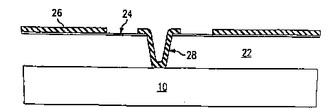
Ihe substrate 10 upo~ which the arrays of devices are built must first be
manufactured with (~MOS addressing ~ . A metal layer, commonly r~fel . ed
to as M3. is then deposited upon the CMOS wafer to form the e~ectrodes. A ~ayer of
10 photoresist is then spun on to act as a spacing materia~ and into which vias are
formed. A thiD metal film 24 with a t~irkn~ss of 500-700 an~;sl~o~s (A) is
depositéd onto of the spacing nl~tP7j , This tbin metal film is then patterned and
etched to form h~ges and the beam which c~nnects the two hin ~e~ for each mirror.
A final metal layer ~s then deposited which nearly romrletely fills the vlas ~ the
1~ spaci~g m~tPri~l to form support posts 28 This layer is p~ttprned and etched to
leave mirrors supported un~l~rne~t~ by a besm of meta~ cnnnected to the hinges.
~hich i~ turn are connecte~ to the support posts.
In order to allow the ~i~l~r~ to move ~ee~y, the spacing m~t~ri~l is etc~ed.
typicallv u~g a pl~qm~ etch, to le~ve an air gap 22 over which the ~or is
2 o suspended. The ent~re array of devices is manufactured on the wafer, resulting in
an a~ay of m1niature movabIe ~ , each oIIe of which can control a pixel in a
Tl-20449 Page 6
2184529
displayed or pri~ted image, among other uses. To form an image, for example, each
mirror is co~tro~led to either direct light towards a display surface or away from the
~ surface. How much light is directed toward~ the surface by each rnirror deterrnines
the brightDess of that pixel. By controlling the entire array in that manner thes image i9 formed.
However, ~is ~lrning of tbe .ui~lol- towards and away from a display surface
reqwres repeated flPYin~ of the hinges }n response to the approp~iate addressings~ This can cause the hinges to become pe~n~nently flexed or ~7~formed in
one direchon or the other, resulting in a degraded picture as the ~Or ~11 always10 direct a small port;ion of the light either to~ ds or away ~rom the screen.
The problem exists even in ~t~te structures su~h as mul~-level DMD
dev~ces su~ as is shown in Figure~ 3a-3f. The multi-level D~ formed with the
~ame iI~itial steps as the single lerel DMD. Figure 3a show~ the initial fnrm~tinn of
the spaciug layer 34 on top of a protective o~ade 32 which covers the electrode layer
30. Electrode layer 30 is on the ~llhstr?~te 10. Vias 36 are cut in t~e ~pacing layer
34, just as iD the single level device.
Thin metal film 24 is then deposited a~ show~ in Figure 3b upon the spaci~g
m~teri~l a~ld into t~e ~ 36 to fosm the posts 28. Thi~ film will form the hingesand beams of the device ju~t as before, but ~n thi~ embodiment they ~rill be on the
2 o elect~cally act~ve level of the device, with the ll~i~l(ir being formed one level a~ove
TI-20449 Page 7
2184~29
_,
them. In the next step, a t~ pr layer of metal is deposited, patte~ned aIld etched
to form hiDge and post caps 36 and a yoke 38 as shown in Figure 3c.
In Figure 3d, this yoke layer of metal is covered with another layer of sp~cing
material 40. A ~ia 42 is fonned in the spacing m ~t~ l directly over the yo~e 38.
s In Figure 3e, the mirror i~ shown after the final metal layer has been deposited,
pattemed and etched to form the mirror 44, which i~ supported by a post 46 formed
iD the via. Finally, the spacing m~t~ l is etehed away, leaving gaps 22a between
the substrate and the active yoke, and 22b between the active yoke and the mirror,
a~ shown m Figure 3f. In this embodiment, the hinges and beam metal film 24 still
0 flex to allow the yoke to deflect in either of two direc~ nc ~Yhen the yoke ~lexes,
the mirror moves as des~red. ~owever, the same problems of permaIlent ~ex or
eform~ion occur.
Previous so~utions to t~is problem have been saught in the formation of the
metal films used for the hinges and ~eam~. The mirror is typically some type of
5 highly Te~ect~ve ~ minum alloy. The beam and hinges have been formed from
titarnum/tun~sten a~loys, with and without impuri~es. ~n eY~mp~e of these types
of a~loys can be found ~n cc~ .ly owned US Patent Applic~ti~n No. 08/395,562.
Additionally, impurities such as nitrogen have been used to strengthen alloys to
produce a better resi~t~n~e to slip, under the theory that the ~l~form~tioD or flex~ng
2 0 of the hiDges was caused by m~croslip. ~ mp~e of these a~loys can be ~ound in
commoDly owned U~ Patent Ap~ n No. 08/339,363.
TI-20449 Page 8
- 218~529
Amorphous m ~tPl i~l is ~lpfinetl by a lack of long range atomic order or atomic
periodicity, such as exhihited by ~ass. Although there can be short range order
between ad3acent atoms, the degree of atomic order decreases with dista~ce, so t~at
there is more uncertaiilty for the position of the third nearest lleighbor atoms, and
5 even more u~certainty for th4 fourth nearest nPiehhor atoms. Amorphous material
can be ~h~r~cte~i~ed by a v~,ely of terhniques including x-ray di~actioll, electron
difflaction, tr~n~mi~ci~n electron mic~)s~y ~ or 'rEM). ~.Y~mplP~ of the x-ray
di~actio~ spectra for ~l~ e~-doped titan~um all~mini~le films which are
amorphous and polycrystall~ne are showIl in figures below. The amorphous fi~m
10 p~hlhjts a single broad peak, while the poly~sl ine film show a sharp peak at
about the same position and a nl~mhçr of other sm~ltsr secondary peaks or secon~-
order rPflecfior~ Both X-ray and electron ~i~dction p~ for amorphous
m:~teri~l s~mrlP.C are ~lnr-~in~t~ by one or two diffilse ling patt~ with llniforr~
~ntensity, whereas cryst~ ne m~tsri~ls shows individual spot patterns or rings of
15 spots which are finer in width. TEM mi~o~-a~hs show a layer of uniform contrast
which does not ~h~n~e ~nth tilt, and no grain bo~lnr~ s or tii.~ ions are
present.
TI-20449 Page 9
~_ 2184S29
~20 -- .
10a -- ~
40 ~ ~ J
Z - .
~7 ~ 5 ~ :~ .o w ._
Z tl~t-
300 ~
:~ 20t~ b
50 ~
1 00 '. ,,~ - -
Z tt~t~
In the applicat~on of the added ~ n impunties, a crystalline structure
was nri~in~lly assunned to be ~lPcir~hle However, upon eXpe~me~tatiOn other
structures were found to have several allv~tages over the non-FCC pol~ y~lalline5 structureori~in~llydesire~ Amorphousa~dnihiripdpo~ i;ne
mul~component alloys other tha~ ~ ...i..~ or ~tanium/tungsten were fo~md to be
superior.
Usi~g reac~ve ~ in~ of the ~ minllm alloy~ produces solid solutions.
dispersion har~ening or amorphous al~o~. ReactiYe nihidin~ ca~l also be used to
10 produce amorphous alloys with m~te~i~l other than ~ minum, for e~carnple, by
using a silicon tltanium target du~ F- These alloy mo~ifir,~ons appear
to produce robust alloy ~inges with ~m~ller grain sizes and also appear to be easier
to etch than ~ta~lium-tungsten-l.iL~ ~ hinges previously use~
TI-20449 Page 10
2184~i~9
-
Using aluminum alloy sputter tar~ets of Al-Si(1%)-Ti(0.~~ d Al~ .5%),
a range of ni~ided alloy filrnc were produced ~nth each target us~llg various
percentages of nitrogen gas added to argon gas used in sputtPring the metal films.
In both systems, at low nitrogen perce~tages of about 10% in the argon sputter gas,
s the polye~ ~talline structure appears to be that of a ~trained AL These films e~hibit
much ~maller grain sizes (~ 100 1000 A) compared to grains i~ Al films without
nitroge~ at ap~ t~ly 1000 10,000 A
At higher ~itrogen percentages, f~rther straining can occur u~til the cryst~l
structure of Al i ~o longer pre-lom-n~nt and amorphous metal is observed. At very
10 high levels of 50% nitro~en in the syu~L~r gas, films appear to be polycryst~lline Al-
N as evidenced ~y coloration due to optical transpa~c~. Gra n sizes in these films
rarlge between 100-200 ~ In the Al-Si(1%at)-lS(0.2%at) alloy ~i~e~s~ed above, the
change from the l?CC crystal sLr~lctur~ to arl amorphou~ crystal structure occurs at
about 15% nitrogen in the argon sputter ga~, while in the Al-T~(0.5%at) alloy the
5 change occurs at between 20%-30% ~trogen in the ~ r gas. This shift
seerningly results from the ~hsenr,e of the 1% Si in the latter alloy.
Low ~itrogen alloys sputtered u~g Al-Si(1%at)-Ti(0.2%at) at about 10%
nitrogen ~ the argon sputter gas pro~ce-l w~Li~g DMD ~evices ~ fewer
defects. One ~ttem~t using 22~ ~uhG~ iD the sputter gas resulted in the
2 o forma~on of whiskers ~llring the ~nne~ling process. Low temperature annealing o~
TI-20449 Page 11
218452~
~tnde alu~ninum alloys which are amorphous tend to grow whis~ers when
annealed at 125-200 ~C, but non-amorphouc alloys do not.
To overcome the formation of whiclrers ~rith the amorphous alloys, a change
was made in the a~loy target used for ~yulle. in~ A CeracT~ Ti(25 at% Ti~ target
5 was used i~ conj~ne~ion ~nth about 10% a~d 50% n~trogen in the sputter gas.
These ni~i~d alloys are amorphous, in~ludingthose w~th ~igher nitrogen alloy
conoPntratio~ which appear to be colored and op~cally transparent. None of these
amorphous alloys were obser~red to form whi~l~p~ during ~nne~ling ~or 24 hours at
200 ~C. Amorphous alloy ~lms ~rere aIso produoed by ~ow temperature deposi*on
10 using this target without int~r-linn~ di*on of nitrogen. Compositional a~alysis
showed the presence of re~ l 0. ,~1;el~ and ,~ o~ at levels of about 1-3% These
impun~es anse from the powder used in man~f~e~lrin~ the Cerac~ target.
it;nn~ly~ ~e ten-ci~e strê~gth of ~ese fi~ms appêars to be improved by
m~kinE them amorphous siIlce there are no slip pla~e~ or disloc~tinTlc for sIip. The
15 sag is controlled by the stress ~stributions of the Al alloy on the spac~ng m~tP~
which can vary with sputter con~ onq High compressive stresses ~ the metal
films deposited on the spacing mateIial tend~ to cause 9~E~ng, whereas tens~le
sL~esse~ tends to prevent 5~gin~ By ~kin~ amorpholls films, the tensile strength
i~ increased. Alloys of Al-Ti (25 a~% Ti) which are sputtered in argon with 0-10%
20 ~ ogen tend to have t~ncile stresses when deposited o~ photoresist and usually do
not sag. ,~ chart of the stress within the metal fil~TI versus the total sputter gas
TI-20449 Page 12
21~29
- pressure is shown in Figure 4, with posit;iYe values denoting a ten~ile stTess. A~
can be seenr films with 0-10% l.i~O~ ~ have little or no compressive stress thereby
resulting in a flat hinge.
Sputtered films of TiALI t~iC~lly ~how residual o~.y~ and ~trogen levels
~ in~ f rom the powdered ta.l ets. Thi~ could be reduced by using a cast target.Nitrogen leveLs in the film can be much ~igh than those ~ the sputter gas. For
example, 10% nitrogen in argon has produced level exceeding 18%at nit~ogen in
the reactively sputtered film. The e~act composili~n depends upon deposition
parameters and con~i1ion.c.
Thelefule, it is de~able to use alloys of TiAll(N) cont~inin~ ~itrogen levels
between about 0.1~5 at% for use as the m~rhs~nir~l or structural members of
devices such as the ~ t~l mic~L~Ir device or other devices which require elasticconnec~gmembersbetween s~ nn51ry andmo~ingparts. Fullynit~ ?dalloy~
are also poPnt~lly useful.
L 5 It may also be des~rable to add impurities to the aluminum nitrogen alloys,
such as .ci7iron~ bûron, g~rm~nillm, u,.y~ . or carbon for the covalent bondi~g ~o a~
to help st~hili7e an amorphous alloy ~nth a possibly ~i~her lec~ysl~lli7~tion
temperature. ~ddition~llyJ otheri~ ies may be de~ such as ni~kel zinc,
magnesium or titanium, to fo~m inter~netallic compounds for st~ength when
2 o matenals are pol~,~y~lal~ine. FY~mI~le~ of these compounds are AlNv, (~13Ti)Nv~
TI-20449 Page 13
_ 218~i29
(Al:(SiTi))N, (Al (Q~Z))Ny~ where y can vary between O and 1.0 and Q and Z are the
impun~es list~d above.
-
A~ n~lly, it may be desira~le to use amorphous alloys of alum~num andn~troge~ (~om 0.0-~0.0 at% N) and one or more impl~ritiPs. These amorphous
5 alloys do not have a penodic l~ re~ are re~i~t?nt to slip by dicloc~ion~ will
produce smootber depoiited film~ and have Lsol;ropic ela~tic properties. Fur~her,
the~e alloys may CQn~ te llitrogen and any other imp~ri~eC exduding ~ minum~
mple~ of t}lese could be TiN, SiN, ~IiSi)N~, and Cl~.Si(~ )NY, where x and y canvary b~lwee~ O and l. For eYqmrle, a Ti:Si:N alloy of approYm~te compos~ion of
0 1:2:3 wa~ deposited by resctive ~ from a pure titqn~ target with
overlaid Si which coveled about 50% of t~e Ti target stlrf^^R and 10% nillu~_~ in
the argon ~ LLt:~ gas.
By COn~nl~inE the c~tr~ ~l aliO~ o~ ~ and 1;t~nillm it i~ po~nhle to
set the pe~c~ ,tages at w~ t;he films ~ecome amorphou~ opposed to
15 polyc~ta~e. Using a target of Al -112% Ti and ~ulle~ gas with argon, f~om 0 to
20 % nitrogen, the film i~ poly~ ~L~lline when ~ull~d u~ing 3 kW power.
Between 20-30 % Diho~ ., the film beconle~ amorphou~. At cono~nt~ ations levels of
nitrogen of over 35%, the film beco~nPs polyc~ llin~. The cn7-rçnh~ation of li
seems to have a~ vt~ ely ~ o-Lional a~ect o~ the conce~ n of nitrogen at
20 which the f& be~o nes amorphous. ~i~her percentq~es of ~t~ium result in a
lower cQnrentration of ni~rogen at which the film becomes ~norphous.
Tl-~0~1~ Page 14
2184~29
However, pol~;,ysla~e m~teri~l.c seem to be useful as well. FJx~mples of
these types ~f alloys wou}d be Al + AlN as well as AlN, and Al (~ 15%at N). The
polycryst~ ne alloys may also be ~ormed usiDg the impurities mentioned above.
The use of polycryst~lline films, w~ile use~. does not seem to be :~s bPnPfiri~l as
s the use of amorphous ~m8 for el~c mpmbers in micromech~nir~l devices. The
amorphous films P-rhihit higher yield strengths, have isotropic elastic properties
and result i~ smoother deposited films.
Ihus, although there has been ~es-,ribed to this point pa~cular
embodiments of an ~mproved elastic micr~Tne(~h~ni~l member, it ~ not intellded
0 ~at such specific ~efere~ces be conei~lpred a~ limit9*nns upon the scope of tbi~
invention except in-so-~ar as set forth in the following ~ imc
TI-2~449 Page 15