Note : Les descriptions sont présentées dans la langue officielle dans laquelle elles ont été soumises.
CA 02192784 1999-04-O1
1
ON SCREEN DISPLAY A_RR NrF~NT
FOR A DIGITAL VIDEO SI ~NA1 PROCES~INCi ~Y~'I'FM
This application is related to Canadian patent
application Serial No. 2,191,556 filed May 30, 1995,
entitled "On Screen Display Arrangement for a Digital Video Signal
Processing System" and assigned to the same assignee as the present
application.
The invention concerns an "on screen display" (OSD)
arrangement for a digital video signal processing system.
On screen display (OSD) arrangements employed in
video processing systems include a switching (or "multiplexing")
network for switching between graphic image representative
signals and normal video signals so that a graphic image can be
displayed on the screen of a picture reproduction device either in
place of the image represented by the video signals or together
with (inserted in) the image. The graphic image can take the form
2 0 of alphanumeric symbols or pictorial graphics, and can be used to
indicate status information, such as channel numbers or time, or
operating instructions.
In an OSD arrangement for use in an analog video
signal processing system, the multiplexing network typically
2 5 operates to switch in levels corresponding to the desired intensity
of respective portions of the graphic image at the time the graphic
image portions are to be displayed. In such an arrangement the
graphic image representative signals take the form of timing
pulses which occur when the graphic image portions are to be
3 0 displayed and are used to control the multiplexing network. Such
an analog OSD arrangement can also be used in a digital video
processing system, but requires that the video signals be first
converted to analog form. While digital video signal processing
systems typically include a digital-to-analog converter section in
3 5 which the digital video signals are converted to analog form, it
may be more cost effective for the OSD arrangement to be
wo 9sr3ss25 219 2 7 8 4 PCT~S95106850
2
incorporated as an integral part of the digital video processing
section.
The invention concerns a digital OSD arrangement for a
digital video signal processing system, and especially one for a
digital video processing system in which the digital video signals
represent image information in compressed form.
More specifically the invention concerns an OSD
arrangement for a digital video processing system which includes
a source of a sequence of digital words representing respective
components of a video image. The video image component
representative digital words are organized in groups
corresponding in a compressed form to more than one picture
element. For example, the groups may correspond to two picture
elements and may include first and second luminance components
corresponding to respective ones of the two picture elements, and
two color difference signals corresponding to each of the two
picture elements. A memory stores digital words representing
respective components of a graphics image. The graphic image
component representative digital words are organized in groups
corresponding in uncompressed form to respective picture
elements. For example, the groups may include the luminance
and a pair of color difference components corresponding to
2 5 respective picture elements. A converter converts the graphic
representative image groups stored in the memory to new groups
of graphic image representative groups which are of the same
form as the video image representative groups to make it possible
to multiplex the video image representative groups and the
3 0 graphics image representative groups. For example, the converter
produces new graphic representative groups which include first
and second luminance components corresponding to respective
ones of the two picture elements, and a pair of color difference '
signals corresponding to each of the two picture elements. A
3 5 multiplexer selects either ones of the video image representative '
WO 95!35625 219 2 7 8 4 PCT~595/06850
3
groups or ones of the graphics image representative groups to
produce a sequence resultant image representative groups.
These and other aspects of the invention will be
described with respect to the accompanying Drawing.
In the Drawing:
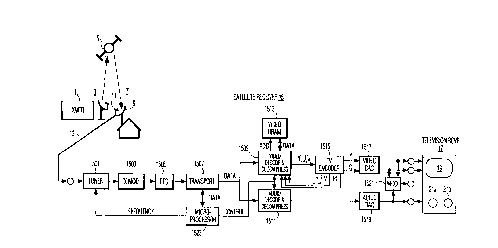
Figure 1 is a block diagram of a digital satellite
television system including a digital signal processing section
including a digital OSD arrangement as an integral part in
accordance with an aspect of the invention;
Figure 2 is a block diagram which disclosed details of
the digital video signal processing section of the digital satellite
television system shown in Figure 1 the digital OSD arrangement;
and
Figure 3 is a block diagram of a converter used in the
OSD arrangement shown in Figure 2.
In the satellite television system shown in Figure 1, a
transmitter 1, with an associated transmitting antenna 3,
2 0 transmits television signals including video and audio components
to a satellite 5 in geosynchronous earth orbit. Satellite 5 receives
the television signals transmitted by transmitter 1 and
retransmits them toward the earth. The television signals
transmitted by satellite 5 are received by an antenna assembly or
"outdoor unit" 7. Antenna assembly 7 includes a dish-like
antenna 9 and a frequency converter 11. Antenna 9 directs the
television signals transmitted from satellite 5 to frequency
converter 11 which converts the frequencies of all the received
television signals to respective lower frequencies. Frequency
3 0 converter 11 is often called a "block converter" since it converts
the frequency band of all of the received television signals as a
block.
The television signals produced by block converter 11
are coupled via a coaxial cable 13 to a satellite receiver 15.
' 3 5 Satellite receiver 15 is sometimes referred to as an "indoor unit"
because it is located indoors. Satellite receiver IS tunes,
WO 95135625 PCT/US95I06850
219274
4
demodulates and otherwise processes the received television
signal as will be described in detail below to produce video and ,
audio signals with a format (NTSC, PAL or SECAM) suitable for
processing by a conventional television receiver 17 to which they ,
are coupled. Television receiver 17 produces an image on a
display screen 19 in response to the video signals and an audible
response by means of speakers 21a and 216 in response to the
audio signals.
The satellite television system shown in Figure 1 is a digital
television satellite system in which television information is
transmitted in compressed form in accordance with a
predetermined digital compression standard such as MPEG. MPEG
is an international standard for the coded representation of
moving pictures and associated audio information developed by
the Motion Pictures Expert Group.
More specifically, within transmitter 1, analog video
signals and analog audio signals are converted to respective digital
2 0 signals. The digital video and audio signals are compressed and
encoded according to the MPEG compression and encoding
standard. The resultant encoded digital signal has the form of a
series or stream of packets corresponding to respective video and
audio components. The type of packet is identified by a header
2 5 code. Packets corresponding to control and other data may also be
added the data stream.
In the MPEG standard, the video information is transmitted
in the form of a luminance (Y) component and two color difference
(U and V) components. For example, the first color difference
3 0 component may represent the difference between the red image
information and the luminance image information (R-Y) and the
second color difference component may represent the difference
between the blue image information and the luminance image
information (B-Y). In addition, the color information is
3 5 compressed because the two color difference components
correspond to more than one picture element. The use of color
W 0 95/35625 PCT/US95/06850
difference components and the sharing of the color difference
components between picture elements reduces the transmission
5 bandwidth.
Forward error correction (FEC) data is added to the
packets in order make the correction of errors due to noise
within
the transmission path possible. The well known Viterbi and
Reed-
Solomon types of forward error correction coding may both
be
advantageously employed. The digital information resulting
from
the compression, encoding and error correction operations
is
modulated on a carrier in what is known in the digital
transmission field as QPSK (Quaternary Phase Shift Keying)
modulation.
Satellite receiver 15 includes a tuner 1501 with a local
oscillator and mixer (not shown) for selecting the appropriate
carrier signal form the plurality of signals received from
antenna
assembly 7 and for converting the frequency of the selected
carrier to a lower frequency to produce an intermediate
2 0 frequency (IF) signal. The IF signal is demodulated by a
QPSK
demodulator 1503 to produce a demodulated digital signal.
A FEC
decoder 1505 decodes the error correction data contained
in the
demodulated digital signal, and based on the error correction
data
corrects the demodulated .packets representing video, audio
and
2 5 other information. For example, FEC decoder 1505 may operate
according to Viterbi and Reed-Solomon error correction algorithms
when Viterbi and Reed-Solomon error correction encoding is
employed in transmitter 1. Tuner 1501, QPSK demodulator 1503
and FEC decoder 1505 may be included in a unit available
from
3 0 Hughes Network Systems of Germantown, Maryland or from
Comstream Corp., San Diego, California.
A transport unit 1507 is a demultiplexer which routes
the video packets of the error corrected signal to a video
decoder
1509 and the audio packets to an audio decoder 1511 via a
data
3 5 bus according to the header information contained in the
packets.
Video decoder 1509 cooperates with a random access
WO 95135625 219 2 7 ~ 4 PCTIUS95/06850
6
memory (RAM) 1513 for example, in the form of a dynamic RAM
(DRAM), to decode and decompress the video packets to form a ,
stream or sequence of digital words representing respective
luminance (Y) and color difference (U and V) components. The ,
sequence of video component representative digital words is
coupled to a television encoder 1515 which converts the
component representative digital words to a sequence of digital
words representing luminance (Y) information and a sequence of
digital words representing chrominance (C) information in
accordance with the line and field raster scanning format of a
conventional television standard such a NTSC, PAL or SECAM.
Television signal encoder 1515 generates line (H) and field (V)
rate signals and a picture element (pixel) clock signal (P) which
are coupled to video decoder 1509 to synchronize the component
representative sequence of digital words. The luminance and
chrominance representative digital words are converted to analog
luminance and chrominance signals by respective sections of a
digital-to-analog converter (DAC) 1517.
Audio decoder 1511 decodes and decompresses the
audio packets and the resultant digital audio signal is converted to
a baseband analog audio signal by a DAC 1519. Although only a
single audio channel is indicated in Figure 1, it will be appreciated
2 5 that in practice one or more additional audio channels, for
example, for stereophonic reproduction, may be provided as is
indicated by speakers 21 a and 21 b.
The baseband analog video and audio signals are
coupled to television receiver 17 via respective baseband
3 0 connections. The baseband analog video and audio signals are
also coupled to a modulator 1521 which modulates the analog
signals on to a radio frequency (RF) carrier in accoidance with a
conventional television standard such as NTSC, PAL or SECAM for
coupling to the antenna input of a television receiver without
3 5 baseband inputs.
W 0 95/35625 PCT1US95/06850
219274
7
A microprocessor 1523 provides frequency selection
control data to tuner 1501 for controlling the operation
of tuner
1501 to tune channels selected by the user. Microprocessor
1523
also operates interactively with transport 1507 to affect
the
routing of data packets. Microprocessor 1523 additionally
provides control data to video decoder 1509 and audio decoder
1511 via a control bus.
Still further, microprocessor 1523 generates control
data for causing graphics images, such as alphanumeric characters
and/or pictorial graphics, for example, representing status
information and operating instructions, to be displayed
on screen
19 of television receiver 17. The graphics data specifies
the color
and position of each picture element (pixel) of the graphics
which
are to be displayed. The graphics data represents a pixel
by pixel
map or "bit map" of the graphic image.
Advantageously, the remaining portion of the on
screen display (OSD) arrangement is integrally incorporated
in
2 0 video decoder 1509 and associated video RAM 1513, which
are
primarily used for the decoding and decompression of the
video
data packets. The graphics data is coupled to video decoder
1509
via the control bus. As a result of the shared use of video
decoder
1509 and associated video RAM 1513, a separate OSD
2 5 arrangement is not needed. Details of the OSD arrangement
will
be described with respect to Figure 2.
Video decoder 1509 is incorporated in a single
integrated circuit (IC). Similar video decoding and decompression
ICs, with the exception of the OSD provisions to be described
3 0 below, are commercially available. For example, a MPEG decoding
and decompression IC, identified by part number ST3240,
is
available from SGS Thomson, of France. While the details
of the
portions of video decoder 1509 concerned with the decoding
and
decompression of the video data packets is not necessary
to
3 5 understanding the OSD provisions, the following brief description
of those portions is helpful.
WO 95135625 PCT/U595/06850
2192784
8
Video decoder 1509 includes a FIFO (first in, first out)
buffer memory 1509-1 which receives video data packets on ,
demand in relatively small segments from transport 1507 and
which couples them in relatively larger segments via a memory ,
controller 1509-3 to a section 1513-1 of RAM 1513 reserved for
decoding and decompression. Video RAM 1513 is addressed
under the control of memory controller 1509-3. Decoding and
decompression section 1513-1 of RAM 1513 includes a rate buffer
section 1513-1-3 for storing the received video data packets and
a frame store section 1513-1-2 for storing frames of video
information during the decoding and decompression operation. A
video image display unit 1509-5 decodes and decompresses the
stored video data packets to form the sequence of video image
component representative digital words (Y, U, V). For this
purpose, video display unit 1509-5 requests data from decoding
and decompression section 1513-1 of video RAM 1513 via
memory controller 1509-3 as required. The generation of the
2 0 component representative digital words is synchronized with the
field (V), line (H) and pixel (PC) rate signals generated by
television signal encoder 1515. Control data generated by
microprocessor 1523 is received by a microprocessor interface
unit 1509-7 and coupled to various portions of video decoder
2 5 1509 via an internal control bus.
The number of bits contained in the video image
component representative digital words determine the number of
possible levels and thereby the resolution of the respective
components. For n-bit words there are 2n possible levels
3 0 corresponding to the 2n possible binary states. By way of
example, in the present embodiment, the video image component
representative word contain eight bits and therefore each
component can have 28 or 256 possible levels. The sequence of
video image component representative digital words is organized
3 5 in groups of components in which each group corresponds to
plurality of pixels in subsampled or compressed form. More
WO 95135625 PCT/US95106850
2192784
9
specifically, in the present embodiment, the video image
representative groups correspond to two pixels, each of which
includes a first luminance representative digital word (Y1)
corresponding to a first pixel, a second luminance representative
digital word (Y2) corresponding to a second pixel, and a single pair
of color difference representative digital words (UI,2 and V1,2)
corresponding to each of the first and second pixels. This has
been referred to as a "4:2:2" format in the digital video signal
processing field. The subsampling or compression of the color
difference signals relates to the image data compression which
occurs in the transmitter 1 for the purpose of reducing the
transmission bandwidth. More specifically, the transmitted image
data is organized in what is known as 4:2:0 format in which the
image representative words correspond to four pixels in which
there are four luminance representative words corresponding to
respective ones of four pixels and a single pair of color difference
representative words corresponding to each of the four pixels.
2 0 The 4:2:0 image representative groups are converted to 4:2:2
image representative groups by interpolation within video display
unit 1509-5. A complete set (4:4:4) of components for each pixel
is produced by interpolation within television signal encoder
1515.
2 5 The OSD portion of video decoder 1509 includes an
OSD controller 1509-9 which cooperates with an OSD section
1513-3 of video RAM 1513. The graphics representative bit map
generated by microprocessor 1523 is coupled via microprocessor
interface unit 1509-7 and memory controller 1509-3 to OSD
3 0 section 1513-3 of RAM 1513 for storage. For each pixel of the
graphic image there is a digital word representing a color for that
pixel. The number of bits contained in the color representative
digital words determines how many different colors each pixel can
have. If the color representative words contain n bits, then each
' 3 5 pixel can have any one of 2n colors corresponding to the 2n
possible binary states of the n-bit color word. By way of example,
WO 95135625 PCT/U59~106850
z~ 9z~~~
in the present embodiment, the color representative words
contain two bits. Accordingly, each graphics pixel can have any
S one of four colors corresponding to the four possible binary states
(00, O1, 10, and 11) of the two-bit color word. The pixel color
information is organized in a component form in which for each
color word there is a unique group of component representative
digital words. The components are selected to be the same as the
10 components used for the transmission of video image information:
namely, luminance (Y) and a pair of color differences signal (U and
V). The selection of the same components for video images and
graphics images simplifies the OSD arrangement because it avoids
the need for conversion from one set of components to another.
For example, in the present embodiment which utilizes two-bit
color words, the following relationship between the color
representative digital words and the groups of component
representative digital words exits:
color group of components
0 0 YA, UA, VA
0 I YB, UB, Vg
10 YC, UC, VC
I 1 YD, UD, VD
The actual color (represented by the subscripts A, B, C
or D in the table) of a graphics pixel depends on the value
represented by component representative digital words of the
respective group. By way of example, in the present embodiment,
2 5 the graphic image component representative words each contain
four bits. Four-bit component representative words provide 16
possible levels for each component. The four bits represent the
most significant bits of an eight-bit word which is eventually
formed by OSD display unit 1509-9, as will be described below.
3 0 The graphic image component representative words -
are transmitted to and stored in OSD section 1513-3 of RAM 1513
w095135625 219 2 7 ~ 4 I'CT~S95106850
11
from microprocessor 1523 in component groups as is indicated in
the table in the form of a header for the bit map. In the present
embodiment, in which each graphic image component
representative digital word contains four bits, each group includes
12 bits. The colors of a graphics image may be changed by
changing the four bits of one of more component representing
words of the header, depending on the nature of the graphics
image to be displayed.
OSD display unit 1509-9 causes the bit map to be read
out from OSD section 1513-3 of RAM 1513, and converts the color
representative word for each pixel to the corresponding
component representative group from the header. For this
purpose, OSD display unit 1509-9 requests data from OSD section
1513-3 via memory controller 1509-3 as required. Since, in the
present embodiment the graphic image component representative
words contain only four bits while the video image representative
words contain eight bits, OSD display unit 1509-9 converts the
2 0 four-bit graphic image component representative words to eight-
bit words by simply adding four binary "Os" as the least four
significant bits to the four-bit words. The generation of the
graphic image component representative digital words by OSD
display unit 1509-9 is also synchronized with the field (V), line
2 5 (H) and pixel (PC) rate signals generated by television signal
encoder 1515.
As earlier noted, the video image component
representative groups generated by video image display unit
1509-5 represent video image information in a compressed form
3 0 in which for every two pixels there are two respective luminance
representative words and one pair of color difference
representative words in a so-called 4:2:2 format. On the other
hand, the graphic image component representative groups stored
in OSD section 1513-3 of RAM 1513 and generated by OSD display
3 5 unit 1509-9 represent graphics image information in an
uncompressed form in which for every one pixel there is one
W095/35625 Pt:TlUS95106850
2192784
12
luminance representative word and one pair of color difference
representative words (or for every two pixels there are two ,
respective luminance representative words and two respective
pairs of color difference representative words). The latter
uncompressed format has become known as the "4:4:4" format in
the digital video signal processing field. The 4:4:4 graphics image
sequence is desirable since it allows as many colors as possible to
be defined with a given number of bits because it provides for a
unique luminance component and two unique color difference
components for each pixel of graphics. However, the 4:4:4 graphic
image sequence is not compatible with the 4:2:2 video image
sequence and cannot be readily multiplexed with it to so as to
insert a graphic image into a video image.
To solve this problem, video decoder 1509 includes an
OSD converter 1509-11 for converting the 4:4:4 sequence used for
the graphic image components to the 4:2:2 sequence used for the
video image components. As is pictorially indicated in Figure 2,
2 0 for every two graphics pixels, converter 1509-11 selects the pair
of color difference components for the first pixel and deletes the
pair for the second pixel. As shown in as shown in Figure 3, OSD
converter 1509-11 may comprise a latch 1509-11-I for storing
two groups of graphic image component representative words,
and a multiplexer 1509-11-3 which selects the appropriate
component representative words in sequence from those stored in
latch 1509-11-1 at the output rate. It is desirable that the
number of 4:4:4 groups of graphic image representative
components per line be an even number because two of the
3 0 original 4:4:4 graphic image groups are used to produce each new
one of the 4:2:2 graphic image groups.
While the output sequence is shown as being, in the
order named, a first luminance (Y) component for a first pixel of
two pixels, a first color difference component (U) for each of the
3 5 two pixels and a second color difference component (V) for each of
the two pixels, and a second luminance component for the second
WO 95135625 PCTIUS95/06850
2192784
13
of the two pixels, other output sequences may be used. For
example, the output sequence may be, in the order named, a first
color difference component (U) for each of the two pixels, a first
luminance (Y) component for a first pixel of two pixels, a second
color difference component (V) for each of the two pixels, and a
second luminance component for the second of the two pixels.
An output multiplexer 1509-13 selects either groups
of video image component representative words provided by
video display unit 1509-5 or groups of graphic image component
representative words provided by OSD converter 1509-11 under
the control of OSD display unit 1509-9. In a video image only
mode of operation, output multiplexer 1509-13 selects only the
video image groups. In a graphic image only mode of operation,
output multiplexer 1509-13 selects only the graphic image
groups. In a "superimpose" mode of operation, in which the
graphic image is inserted within a video image, output multiplexer
1509-13 selects either the video image groups or the graphic
2 0 image groups on a pixel by pixel basis. The 4:2:2 output sequence
of component representative words produced by output
multiplexer 1509-13 is coupled to television signal encoder 1515.