Note : Les descriptions sont présentées dans la langue officielle dans laquelle elles ont été soumises.
~~C~'. ~'U\:E?H'r\-Vll:Gl,C;i(~.V c):3 : (.(._ (_J,
CA 02208762 1997-06-25 S(~it315~ +.6J t3.) ~>,3~J~~6~l~E3F~:~ 5
fT~AT P ,T, T~GZNG bEVICE
Field of the Tnvention
This in~crention relates in general to thin film
transistors (TFTs) and more particularly to a pair of
novel TFT structures exhibiting reduced parasitic
capacitance.
Background of the Invention
As a consequence of recent rapid development of flat
panel display technologies, thin film transistors (rFTs)
are being actively utilized in the implementation of two
types of large area electronic devices, namely liquid
crystal displays (LCDs) and flat-panel imaging devices.
These devices generally comprise a large number of TFTs,
which act as switches or atrrplifiers.
Aa is well known i.n the art, a typicalTFT is
constructed using a MOS structure (metal oxide
semiconductor) co~npris~,ng a semiconductor film, a gate
electrode, a gate dielectric film, source and drain
electrodes. The semiconductor film can be fabricated
from amorphous silicon (a-Si), poly-silicon (poly-Si),
cadmium selenide (CdSe7, or other suitable semiconductor
material. The metal material of the electrodes can be
fabricated from chromium or aluminium. The material of
the dielectric film is fabricated typically from one of
either silicon nitride, silicon oxide pr various anodic
oxide films.
,. As is well known, MOS transistors are normally
provided with an overlapping area between the gate and
source and between the gate and drain electrodes, to
ensure continuity of the channel formed in the
semiconductor layer. Generally, the overlapping area
should be no less than the design rule of a particular
TFT device. Tworparasitic capacitances (Cgs and Cgd) are
formed in the overlapping areas between gate and source
and between gate and.drain, respectively. As a
~M~r~oEn s~~Er
CA 02208762 1997-06-25
WO 96/22616 PCT/CA95100030
2
consequence of these known parasitic capacitances, gate
control pulses are known to feedthrough the semiconductor
layer into the source or drain, thereby deteriorating
switching performance. While this is a well known common
problem for all MOS transistors, the problem is
exacerbated in large area TFT matrix applications where
design rules must provide sufficiently large tolerances,
corresponding to the lithographic tolerances of the
fabrication process on a large size exposure area.
When a TFT switch turns off, the feedthrough charge
comes from two components. The first is the differential
component of the gate pulse on the parasitic capacitor,
and the other results from channel electrons which are
split away and squeezed into the source and drain
electrodes (Z.S. Huang, Y. Katayama and T. Ando, " The
dependence of the parasitic capacitance and the reset
potential level in a solid-state imaging sensor,"
Proceedings of the Joint Meeting of 1989 Electric &
Electronic Institutes, Tokai Shibu, Japan, P. 325,
October (1989) and Z.S. Huang and T. Ando," An analysis
of reset mechanism in a stackec. and amplified imaging
sensor," Journal of the Institute of Television Engineers
of Japan, Vol. 46, no. 5, pp. 624-631, May (1992)).
For a TFT-LCD, when the TFT turns off, negative
charges are left on the pixel capacitor, causing the bias
voltage of the liquid crystal to drop. This is
equivalent to applying a DC voltage directly on the
liquid crystal. This DC bias voltage causes the
characteristics of the liquid crystal to shift in one
direction, causing crosstalk. Moreover, because the
capacitances of a liquid crystal in the ON and OFF states
are different, feedthrough charges generate different
feedthrough voltage shifts for "white" and "black"
pixels. This causes image sticking and flicker noise in
the TFT-LCD, a phenomenon referred to as "image
persistence" in I-Wei Wu, "High-definition displays and
technology trends in TFT-LCD", Journal of the SID, 2/1,
CA 02208762 1997-06-25
WO 96/22616 PCT/CA95/00030
3
pp. 1-14 (1994).
_ The problem of feedthrough charges in TFT LCD
' applications is less serious when compared to the problem
of feedthrough charges in imaging sensors since the
S signal voltage is extremely small. Feedthrough charges
in imaging applications can result in saturation of the
feedback capacitor in the readout charge amplifier of a
.
TFT matrix causing latch-up of the amplifier. One
solution to this problem involves incorporating a larger
feedback capacitor in the charge amplifier. However,
that approach sacrifices the sensitivity of the
amplifier, as discussed in I. Fujieda et al., ~~High
sensitivity readout of 2D a-Si image sensors,~~ Japanese
Journal of Applied Physics, Vol. 32, pp. 198-204 (1993).
Furthermore, feedthrough charges in imaging
applications affect not only the source or output portion
of the TFT but also the drain or pixel electrode portion.
In this case, excessive negative charge fed into the
pixel capacitor can prevent the TFT from turning off so
that charge leaks into the data line. For high-level
incident light or radiation, the leakage current drops
quickly, whereas for low level light or radiation, the
leakage current can remain high before a subsequent
charge readout. This can result in crosstalk or smearing
of the image along the data line and a consequential
deterioration of image quality.
Several TFT structures and specialized driving
schemes have been proposed to alleviate the problem of
image quality deterioration caused by charge feedthrough
in TFT arrays. The most common prior art approach
involves incorporating an additional storage capacitor i
n
each pixel of the TFT array. However, that approach
suffers from the disadvantage of decreasing the fill
factor of the TFT imager or LCD and increasing the
probability of an interlayer short circuit.
Self-alignment fabrication processes constitute
another approach to reducing parasitic capacitances.
RC1. VUn,:tl':1-VII:L~,C:HL:\ Ua3 : L.L._ L -.CA 02208762 1997-06-25 SiVIBI:S-
a +4,3 g.3 .? c
_«-.~ ~. . ~« . c r ~ ;3,3~J~b~~65:1~ Ei
4
Using self-aligned techniques, a channel length cdll be
created which is almost exactly the same length as the
bottom gate by using the bottom gate pattern as a photo-
mask and flooding the backside of the glass substrate
with ultraviolet light, as discussed in the reference of
I-Wei Gnu cited above. There are two known types of self-
alignment TFT structures. The first is referred to as
the "non-complete~~ self-alignment type TFT, which is
capable of reducing parasitic capacitance but incapable
of removing it completely. The second is referred to as
the incomplete" self-alignment type TFT, in which lift-vff
techniques are utilised. However, the lift-off
techniques contribute to complexity of the fabrication
process and Cannot be used for a top gate TfT structure,
which i9 the preferred structure for many imaging sensors
such as the amorphous selenium/cadmium selen:ide TFT
SAMURAI radiation imaging sensor (W. Zhao and J.A.
Rowlands "A large area solid-state detector for radiology
using amorphous selenium," SPIE Vol. 1&51, Medical
Imaging vT; Instrumentation, pp. 134-143, (1992)).
In terms of prior art driving schemes, four kinds of
LCD driving methods (Frame inversion, Gate line
inversion, Data line inversion and Dot invezsion method)
have been proposed (Reference: I-Wei Wu, "High-definition
z5 displays and technology trends in TFT-LCDS," Journal of
the SID, vol. 2, no. 1, pp.l-14, 19~g), These driving
methods change the polarity of bias voltage on the liquid
crystal film periodically, and they reduce the sticking
and crosstalk effects by averaging noise in the time or
spatial domains. However, none of these is capable of
.. driving an imaging sensor, because changing polarity of
bias voltage on a detector film is usually not allowed.
Most of these prior art photodetectors.do not show
symmetric characteristics as altering the polarity of
35 bias voltage. Furthermore, it is difficult to change the
polarity of bias voltage in, some X-ray detectors such as
a-Se or a-si x-r~,y detectors, where the bias voltage can
be tens of KV.
AwIEfJDED Sl-iEET
ttC~.V<)V:E=:P:\-~llh~~;C:lilW U:3 :14- L-97CA 02208762 1997-06-25 SIJIt3l:S-~
+~1.J $9 ~>a3:3:J4~~LE35:11 r
Another prior art approach to solving the problem of
parasitic aapacitancee zs the use of a dual gate M~SFET
comprising two series connected FETs fabricated on a
silicon substrate (N. Ditrick, M.M. Mitchell and R.
5 Dawson, "A low power MOS tetroden, proceedings of
International Electron Device Meeting, 1965). This
device is known to be characterized by relatively low
switching noise. When the dual gate FET is used as a
switch, one gate is grounded and the other gate is
1p connected to a gate control pulse for turning on and
turning aft the switch. Since the feedthrough charge is
shunted to ground for the control gate, the capacitance
Cgd equals zero. However, this dual gate structure
cannot be applied to TFT-CDs or TFT image senRO.rs
without decreasing the fill-factor.
Neither the self-alignment type TFT nor the dual.
gate '~.'~~T discussed above, eliminate feedthrough resulting
from split channel electrons.
In addition to the problems mentionPri above, the
split channel electrons also cause partition noise in the
imaging sensors, as described by N. Teranishi et al in
the paper: ~~Partition noise in CCD signal detectwon,~~
IEEE Trans. on.Electron Devices, vol. 33, no. 17., pp.
1696-1701. The partition noise ie proportional to the
Is channel area, in which e~,ectrons are pumped in and pumped
out.
.7
Summa of the Invention
According to ane embodiment of the present invention
a novel TFT structure is provided which is characterized
by no parasitic capacitance on either the drain or the
source electrodes. According to this embodiment, a
triple gate TFT is provided i,n an open gate structure
35 (i.e. the top gate is shorter than the distance between
source and drain electrodes). Two bottom gates are
provided, preferably in the form of metal strips, which
are aligned with the two gaps between the source and top
gate and between the~drain and tap gate, respectively.
f,v~rCNOED SHEET
I~C\'. V<)N:1?F'~\-llI:LVCHW U:3 : L-1~- 1-;37CA 02208762 1997-06-25 -
5111131:J-» t~.[.;) t3;) ~.';3J;)~b~L~Eiu:H E3
6
As an alternative to depositing two gates on the bottom
of the TFT, such gates can also advantageously be
deposited over the top gate. During imaging operation
and readout, the two additional gates are connected t~ a
voltage source for turning on the channel areas covered
thereby.
Parasitic capacitance de~relops between the bottom
gate and source drain electrodes, and the bottom gate and
the top gate. However, since there is no overlapped area
~ between top gate and source and drain electrode, the
parasitic capacitances between them are negligible.
Since the battorn gate is connected to a predetermined
voltage (e.g. actual ground) during operation, there is
no charge fed into the pixel or data line through the
parasita.r: capacitance between bottom gate and souxoe or
drain electrode. A gate control pulse is applied to the
top date to turn i-rA ~,t.~; r~r
- _ _ - __--- -_.--.~ w ... y."~t V11 v1. V1 L .
According to a second~embodimc~nt of the present
invention, a navel TFT switch is provided having
2~ extremely small split charge to the drain terminal, for
use in an image sensor. This TF2' design is referred t.o
herein as a full-transfer TFT switch. Thie switch
comprises a part~.al top gate overlying a portion of the
TFT channel and a portion of the pixel electrode of the
conventional bottom gate TFT. The partial top gate i$
biased to a suitable voltage to create a triangle-shaped
charge density distribution in the TFT channel. Most
channel electrons are therefore repelled by the
triangular potential barrier toward the source e7.ectrode,
with only a very small portion of channel electrodes
splitting away and flowing into the drain electrode (i.e.
the pixel electrode in an image sensor), .
Brief Description of the Drawings
~:;~;~~J~~~ ~~-~~~~r
CA 02208762 1997-06-25
WO 96/22616 . PCT/CA95/00030
7
A detailed description of the two principal
embodiments of the present invention is provided
' hereinbelow with reference to the following drawings in
which:
Figure la is a cross section view of a single pixel
of a prior art TFT array used in a TFT-LCD or TFT imaging
sensor, and Figure 1b is an equivalent circuit for the
TFT structure of Figure la;
Figure 2 is an equivalent circuit of a TFT imaging
sensor with triple gate TFT switch in each pixel,
according to a first embodiment of the invention;
Figure 3 is a layout of a single pixel with the
triple gate TFT of Figure 2;
Figure 4 is a cross-section view through the lines
A-A in Figure 3;
Figure 5 is a cross-section view of a radiation
imaging sensor pixel with full transfer TFT switch in
accordance with a second embodiment of the invention;
Figure 6 comprises parts a, b, and c, and shows
potential well diagrams for explaining the operating
principles of the prior art normal switch of Figure 1;
and
Figure 7 comprises parts a, b, and c, and shows
potential well diagrams for explaining the operating
principles of the full-transfer switch of Figure 5.
Detailed Description of the Preferred Embodiments
With reference to Figure la, a cross-sectional view
of a prior art pixel is shown for use in a TFT-LCD or TFT
image sensor. This prior art TFT structure combrises a
glass substrate 1, a gate 2 deposited on the glass
substrate, a gate insulator 3 deposited over the gate 2,
a layer of semiconductor 4 deposited on the gate
insulator 3 and overlying gate 2, a passivation layer 5
deposited on semiconductor layer 4, a contact layer 6
deposited on the semiconductor layer 4 and passivation
CA 02208762 1997-06-25
WO 96/22616 PCT/CA95/00030
8
layer 5, and source and drain electrodes 7 and 8
deposited on the contact layer 6. An ITO layer 9 is
connected to drain 8 for extending over the pixel area.
The equivalent circuit is illustrated in Figure 1b,
f»rthaY C~ncsine-r ~-ire ~~~r~rve ~~rw..~i..~... n ~t_~ i_ _
r-r waVa rr.aVpill~ VliG .7l~ViGlyc v,.a~rcW ,ll.Vi. ~.,t V:CJ1111eGGeQ LO 3
bias voltage V~,. V~~, is at ground or other predetermined
potential level, if an independent metal line is used for
the storage capacitor. Source 7 is shown connected to a
readout line for conveying an output voltage V,, and gate
2 is connected to a control line for receiving control
pulse V$ for enabling the transistor. The three parasitic
capacitors are illustrated: C~,, Cad, C~,. The pixel
voltage on ITO layer 9 is designated in Figure 1b as V~~.
The capacitor C~ represents the capacitance of liquid
crystal overlaid on one pixel area of the TFT panel.
Turning to Figure 2, an equivalent circuit of the
triple gate TFT structure of the first embodiment of the
present invention is shown in an imaging array. The
array comprises a plurality of readout columns 10
connected to an amplifier/multiplexer 1l, and a plurality
of gate lines 12 connected to a vertical scanner (gate
driver) 22. Each pixel includes a triple gate TFT switch
13, discussed in greater detail below with reference to
Figures 3 and 4. The drain of TFT switch 13 is connected
to one terminal of a selenium radiation detecting
capacitor 14 and one terminal of a storage capacitor 15.
The other terminal of selenium capacitor 14 is connected
to a source of high voltage V~" while the two bottom
gates of TFT switch 13 are connected to the second
terminal of storage capacitor 15 and an additional source
of bias voltage V, via line 16.
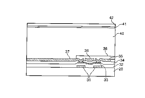
Turning to Figure 3, the layout is shown of a single '
pixel for the imaging sensor of Figure 2. Figure 4 is a
cross-section through the line A-A in Figure 3. A pair '
of bottom gates 31 are disposed on a glass substrate 20,
and a gate insulator 32 is deposited over the bottom
gates 31, as shown in Figure 4. Next, a layer of
CA 02208762 2002-04-09
semiconductor :3~? is deposited over the bottom gatE=s 31
and a passivation layer 34 is deposited and patterned for
source and dra:m:. access. e~ource electrode 35 and drain
electrode 37 a re then deposited on passivation layer 34
5 and extend thr~:~u.gh respective vices to contact
semiconductor i_a~yer 33. Drairn e~.ectrode 37 extends to
form a pixel electrode 37 (Figure 3). A top gate 36 is
deposited over ~,ass.i.vation layer 34 intermediate t:he
source and drain electrodes 3~~ and 37 according to an
10 open gate struc::tu.re. Top gate 36 contacts the horizontal
gate line 12 through contact via 39.
A layer o>= amorphous selc=nium is deposited over the
entire TFT mat~wix to a thickness of approximately 300~m.
Next, an inject:.i_en blocking layer 41 is deposited over
15 the amorphous :selenium layer, and a top electrode 42 is
deposited over the injection blocking layer. The
blocking :layer 41 reduces charge-injection from top
electrode 42, and therefore decreases the dark current of
the a-Se .f.ilm. The t~echnalogy is discussed in greater
20 detail in:Eiich:i Maruyama, "Amorphous built field effect
photoreceptors," Japanese Joux°nal of Applied Physics,
vol. 21, no. 2, p.p. 213-223, 7.982.
The passivation layer 38 covers the entire area
except the pixE:~l. electrode 3'7, which allows
25 photogenerated charges to arrive at the pixel electrode
37 and pratect; the other area elements such as the TFT
switch. In Figure 3, a large hale is shown through
passivation layer 38 on the pixel electrode 37.
In operat:i..on, a high voltage is applied between the
30 top electrode 42 and pixel electrode 37. Electron-hole
pairs are genex:ated in the amorphous selenium layer 40 in
response to exposure to radiation (e. g. x-rays). These
free charges dwift tawards _respective ones of the
electrodes 42 and 3%'. Accordingly, charges collected on
35 pixel electrode 37 are proport:ianal to the amount of
radiation inc:id.e~:zt upon amorphous selenium layer 40, on a
per pixel basis. Charge is read aut from the pixel 37 in
CA 02208762 1997-06-25
WO 96/22616 ' PCT/CA95/00030
response to enabling the TFT switch via a control pulse
on the top gate 36. As discussed above, with the open
gate structure of Figures 3 and 4, source and drain
parasitic capacitances between the top gate 36 are
5 completely eliminated. In order to ensure complete
conduction of the semiconductor layer 33 throughout the
transistor channel, a suitable potential V, is applied to
the bottom gates 31 during the image readout.
Turning now to the embodiment of Figure 5, like
10 numerals denote the same components as illustrated in
Figures 2, 3 and 4. As an option, a blocking layer of
charge injection can be added to the cross-section view
of Figure 5 for decreasing the dark current of the a-Se
film.
Instead of utilizing an open gate structure as shown
in Figures 3 and 4, this embodiment utilizes a
conventional TFT structure with single bottom gate 31
extending beneath the length of semiconductor layer 33.
However, in this embodiment, a narrow metal strip 36
(i.e. partial top gate) is deposited on passivation layer
38 partially covering the TFT channel and the pixel
electrode 37. Partial top gate 36 is biased to an
appropriate potential by connecting it either to an
adjacent pixel electrode or to an independent bias line
(not shown).
Turning to Figures 6a, 6b and 6c, potential well
diagrams are shown for a conventional TFT switch. In the
ON state (Figure 6a), electrons are trapped in the
potential well created in semiconductor layer 33 via gate
31. The depth of the well is governed by the gate
voltage Vg minus the transistor threshold voltage V~.
When the conventional TFT switches from the ON state to '
the OFF state, channel electrons are squeezed towards
both the drain and source electrodes as shown in Figure
6b, with the OFF state potential well diagram being as
shown in Figure 6c.
In accordance with the full transfer TFT switch
CA 02208762 1997-06-25
WO 96/22616 . PCT/CA95/00030
11
structure of Figure65;~the voltage of applied to partial
top gate 36 is adjusted so as to create a triangle-shaped
charge density distribution in the TFT channel, as shown
in Figure 7a. Consequently, as the transistor switches
from the ON state through transition to the OFF state,
the majority of channel electrons are pushed by the
triangle-shaped potential barrier toward the source
electrode 35, as shown in Figure 7b, with only a very
small portion of channel electrons splitting away and
flowing into the drain or pixel electrode 37. The OFF
state potential well diagram for the full transfer TFT
switch of Figure 5 is shown in Figure 7c.
A person skilled in the art understanding the
present invention may conceive of other embodiments and
modifications thereof without departing from the sphere
and scope of the invention defined by the claims appended
hereto.