Note : Les descriptions sont présentées dans la langue officielle dans laquelle elles ont été soumises.
CA 02211467 1997-07-25
P3agneTek s . p . a . ..
"Inverter for the power supply of discharge lamps with
means for improving the power factor"
Description
Field of the invention
The present invention relates to an inverter
device for the power supply of an electrical load, in
particular of a discharge lamp.
Prior art
Devices of this type are described for example a.n
GB-A-2,124,042, EP-A-0 667 734, EP-A-0 488 478, US-A-
5,426,344.
These devices have a rectifier powered by an AC
source, for example the standard electrical mains. In
parallel with the rectifier bridge (see for example GB-A
2,124,042) there is provided a filter capacitor and a
smoothing capacitor for supplying a substantially DC
voltage to an inverter circuit section, comprising
controlled switching means for powering a load with an
oscillating circuit at a high-frequency voltage. A diode
is interposed between the rectifier bridge and the filter
capacitor on the one hand and the smoothing or "bulk"
capacitor on the other.
Circuits of this type must exhibit a high power
factor as close as possible to one and a limited crest
factor. Power factor is understood to mean the ratio of
active power to apparent power, while crest factor is
understood to mean the ratio of the maximum value of the
current in the load to its root-mean-square value and
measures the amount of fluctuation, at a frequency
typically doublev the frequency of : the AC supply, 'of the
peak value of the current at the load. In inverters for
the power supply of discharge lamps the oscillation in
the peak value of the load current is detrimental since
it reduces the lifetime of the lamp.
The object of the present invention is the
production of an inverter device which makes it possible
to alleviate the drawbacks of conventional devices.
CA 02211467 2004-12-14
20333-413
2
In particular, the object of the invention is to
produce an inverter circuit of the type mentioned above
which exhibits a greater power factor than conventional
circuits.
A further object of an improved embodiment of the
invention is the production of a circuit with a reduced
crest factor, and in particular a circuit in which it is
possible to increase the power factor and reduce the crest
factor independently of one another.
Summary of the invention
These and further objects and advantages, which
will become clear to those skilled in the art from reading
the following text, are achieved with an inverter circuit of
the type mentioned above, in which, in the power-supply
section, in series with the rectifier bridge supplied by the
AC voltage source, there is arranged an inductor with a
value such that the said power-supply section exhibits a
predominantly inductive behaviour towards the load. The
predominantly inductive behaviour thus achieved causes the
inverter and the load powered by it to see a source of
current instead of a source of voltage, as in conventional
circuits, with a consequent improvement in the power factor
of the device.
Accordingly in one aspect of the invention, there
is provided, an inverter device for the power supply of a
load comprising: a power supply section with means of
connection to an AC voltage source and two poles for
connection to an inverter section, said power-supply section
comprising a rectifier bridge powered by said AC source and
said inverter section
CA 02211467 2004-12-14
20333-413
2a
comprising a half bridge arrangement of controlled switching
means for supplying a high frequency voltage to said load
through a resonant circuit connected to said inverter
section; in parallel with said rectifier bridge and said
half bridge arrangement, a filter capacitor and a smoothing
capacitor for supplying a substantially continuous current
to the inverter section, a unidirectional component being
arranged upstream of the smoothing capacitor and downstream
of said filter capacitor; said half bridge arrangement, said
filter capacitor and said smoothing capacitor being arranged
across said poles through which the inverter section is
connected to said power supply section and said load being
connected to the centre of said half bridge and to a pole of
said filter capacitor characterized in that said power-
supply section includes an inductor arranged in series with
said rectifier bridge, connected upstream of said half
bridge arrangement and upstream of said resonant circuit
said inductor having a value such that said power-supply
section exhibits a predominantly inductive behaviour towards
the inverter section.
The inductor indicated above can be arranged
upstream or downstream of the rectifier bridge.
An auxiliary capacitor which resonates with the
said inductor when the voltage across the terminals of the
rectifier bridge passes through the zero value can
advantageously be arranged between the inductor and the
inverter (consisting for example of a half-bridge structure
with two high-frequency controlled cutouts). This makes it
possible, as will clearly be seen below with reference to an
illustrative implementation of the invention, to reduce the
crest factor independently of the power factor.
CA 02211467 2004-12-14
20333-413
2b
Upstream of the rectifier bridge, between it and
the AC voltage source, there is also advantageously
provided, in a manner known per se, an EMI filter
(electromagnetic interference filter) against conducted
CA 02211467 1997-07-25
- 3 -
noise, with a cutoff frequency typically greater than
kHz.
Further advantageous characteristics and imple
mentations of the invention are indicated in the
5 attached dependent claims.
Brief description of the drawings
The invention will be better understood by
following the description and appended drawing, which
shows a practical non-limiting exemplification of the
lOl invention. In the drawing:
Fig. 1 shows a schematic of a circuit according
to the invention, in a first implementation;
Figs. 2 to 6 show the five successive phases of
operation of the circuit of Fig. l;
15' Fig. 7 shows a modified implementation of the
device according to the invention;
Fig. 8 shows an improvement of the device accord-
ing to the invention with an auxiliary resonant
capacitor;
Figs. 9 and 10 show two diagrams indicating the
profile of the current in the inductor in series with the
rectifier bridge in the implementation of Fig. 7; and
Figs. 11, 12 and 13 show three diagrams with the
profile of the current in the inductor, of the voltage
across the terminals of the rectifier bridge and of the
current in the auxiliary resonant capacitor, these being
obtained in a simulation of the circuit of Fig. 8.
Detailed description of the invention .
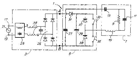
Fig. 1 shows a first implementation of the device
according to the invention. The circuit, indicated
generally as 1, has a first power-supply section
indicated overall as 3 and an. inverter section 5 to which
is connected a load 7, in the example a discharge lamp
represented by a resistor 3 whose electrodes are connec
ted together by a capacitor 11. Indicated as 13 and 15
are a capacitor and an inductor defining a resonant
_ circuit connecting the load to the inverter section 5.
The power-supply section has two terminals 17, 19
for connection to an external AC voltage source 21, for
CA 02211467 2004-12-14
20333-413
- 4 -
example the standard 50 Hz, 220 V (or 60 Hz, 110 V)
electrical mains. An EMI filter 23 with an inductor
component, of a type known per se, is interposed between
the mains power and the circuit. The AC voltage from the
mains is rectified by a rectifier bridge 25, in which the
two output poles connected to the inverter section 5 are
indicated as A and H. In parallel with the rectifier
bridge 25 is arranged a filter capacitor 27, and a second
capacitor 29, indicated hereafter as a bulk or smoothing
10' capacitor, is connected in parallel with the rectifier
bridge 25 with the interposition of a unidirectional
component represented by a diode 31 between the positive
pole of the rectifier bridge 25 and a terminal of the
bulk capacitor 29. The bulk capacitor 29 supplies a
substantially constant voltage to the inverter section.
The ratio of the capacitances of the capacitors 29 and 27
is of the order of 100 : 1 to 10, 000 : l and typically
around 1000 : 1. The capacitor 27 can be arranged
upstream of the rectifier bridge 25 and/or combined with
a further capacitor upstream of the bridge.
The inverter has, furthermore, switching means
represented by a half-bridge arrangement schematized by
two controlled cutouts (typically two transistors)
indicated as 33 and 35 in parallel with respective diodes
37 and 38 . The half-bridge is controlled in a meaner
knows per se via a circuit (not shown) for supplying the
load 7 with a voltage at high frequency, typically of the
order of a few teas of k8z .
Arranged in series with the rectifier bridge 25
is an inductor 39 which, in the example of Fig. 1. is
subdivided into two windings arranged respectively on the
input arm and on the output arm of the rectifier bridge,
between the latter and the filter 23. The value of this
inductor is such that the power-supply section 3 is seen
by the inverter section 5 as a predominantly inductive
source, i.e. basically, virtually a source of current
rather than, as in conventional circuits, a source of
voltage. The value of the inductor 39 is therefore
markedly different from the value of the inductive
CA 02211467 1997-07-25
- 5 -
component normally provided in the filter 23.
The behaviour of the circuit of Fig. 1 in its
various operating phases will now be described with
reference to Figs. 2 to 6, which show the circuit
elements active in each phase. The current flowing in the
circuit will be indicated as follows: IL indicates the
current in the load 7, and Ii indicates the current input
to the inverter section, i.e. the current at the
terminals A and B of the rectifier bridge 25; I~= indi-
1Q Gates the current at the filter capacitor 27. The direc-
tions of the currents are indicated in the various
figures. Furthermore, V~r indicates the voltage across the
filter capacitor 27 and Vb the voltage across the smooth-
ing or bulk capacitor 29.
T5 The first operating phase is illustrated in Fig:
2: the cutout 33 is open and the cutout 35 is closed. The
load current at the initial instant (IL(0)) is zero.
During this phase the current I~r which flows through the
capacitor 27 is given by the difference between the load
20 current IL and the input current Ii. The capacitor 27
discharges (V~= decreases) if IL-Ii is positive, whereas it
charges if the opposite is true. In this phase both
conditions may occur.
This first phase ceases when the circuit for
25 controlling the switching means opens the controllable
cutout 35.
In the second phase, illustrated in Fig. 3, both
cutouts 33,.35 are open. The load current Iz flows in the
same direction as the previous phase, since the circuit
30 is functioning above the resonant frequency. The current
IL flows through the diode 37 and the bulk capacitor 29.
The load circuit 7 transfers energy to the bulk capacitor
29.
This second phase ceases when the value of the
35 load current IL passes through zero and reverses its
direction.
The third phase is represented by the schematic
of Fig. 4: the cutout 33 is closed while the cutout 35 is
open. The load current at the initial instant (IL(0)) is
CA 02211467 2004-12-14
20333-413
- 6 -
zero. The bulk capacitor 29 delivers energy to the
resonant load circuit, while the capacitor 27 is charged
with a current I~= = Ii - Iz which flows in the direction
indicated in the schematic. The voltage across the
capacitor 27 increases until it reaches the value of the
voltage of the bulk capacitor 29. At this instant the
diode 31 becomes conducting and the fourth phase of the
operating cycle of the circuit begins.
The fourth phase is illustrated in Fig. 5. The
diode 31 is conducting, the cutout 33 is closed while the
cutout 35 is open. The voltages across the capacitors 27
and 29 are equal. The load current IL flows through the
diode 31 and the cutout 33, while the input current Ii
flows through the diode 31 into the bulk capacitor 29 and
charges it. The fourth phase ends and the fifth and last
phase begins when the control circuit opens the cutout
33.
The fifth phase is shown in the schematic of Fig.
6. Both the cutouts 33 and 35 are open, While the diode
38 is conducting. The current ID which flows iato the
bulk capacitor 29 is given by the sum of the load current
Iz and the input current Ii. This phase ceases when the
control circuit closes the cutout 33 so as to recommence
the first phase.
The same succession of phases takes place in a
circuit in which the inductor 39 in series with the
rectifier bridge 25 is arranged between the latter and
the inverter section 5, rather than between the rectifier
bridge and the input filter 23. Such a configuration is
shown in 9'ig. 7 where identical numerals are used to
indicate parts in this circuit which are identical to or
correspond with those of Fig. 1. By comparison with the
previous solution, a unidirectional element, represented
by the diode 41, is provided in parallel with the filter
capacitor 27- in order to avoid inversion of the
polarization of the latter.
In the circuit now described the current in the
inductor 39 versus time has the profile indicated
qualitatively in Figs. 9 and 10, where the diagram of
CA 02211467 1997-07-25
_ 7 _
Fig. 10 is an enlargement of the intermediate region of
oscillation between the two half-waves indicated in the
diagram of Fig. 9. It will be observed from the diagrams
of Figs. 9 and 10 that, as the mains voltage passes
through zero, the current in the inductor undergoes a
discontinuous profile oscillating at a frequency equal to
the switching frequency of the inverter. This happens
because as the mains voltage passes through zero, the
energy accumulated in the inductor 39 is low and is
lOl transferred to the bulk capacitor 29 before the end of a
switching period. The current IL in the load circuit
reaches a~ peak precisely as the mains voltage passes
through zero. This happens because in these time
intervals the filter capacitor 27 is charged and
15- dis-charged by the load current IL alone and hence is; for
almost the whole of the switching period, in series with
the capacitor 13. The overall capacitance of the series
arrangement of the capacitors 27 and 13 is approximately
equal to the capacitance of the capacitor 27 alone, whose
20 value is much less than the value of the capacitor 13.
This brings about a rise in the resonant frequency of the
LC resonant circuit which powers the load 7, the circuit
consisting of the elements 13, 27 and 15. As the resonant
frequency rises and approaches the switching frequency,
25 it brings about an increase in the current in the load
and hence an increase in the crest factor. The greater
the value of the impedance 39, the greater this increase.
Hence, if on the one hand the power factor of the circuit
is improved by a high value of the impedance 39, then on
30 the other hand this brings about a deterioration in the
crest factor. Therefore, choosing the value of the
impedance 39 becomes a matter of compromise between the
two effects .
The improved configuration of the circuit of Fig.
35 8 makes it possible to overcome this limitation since the
addition of an auxiliary capacitor 43 (with a correspond
ing diode 45 which prevents the inversion of its polar
ization) in series with the impedance 39 uncouples the
two phenomena, as will become clear from what follows.
CA 02211467 1997-07-25
_ g _
In the circuit of Fig. 8 (in which elements
identical to or corresponding with those of the circuits
of Figs. 1 and 7 are indicated with the same reference
numerals) the capacitor 43 constitutes, together with the
inductor 39, an auxiliary resonant circuit. When the
mains voltage, i.e. the voltage across the rectifier
bridge 25, passes through zero, the capacitor 43
resonates with the inductor 39 and diverts current from
the filter capacitor 27. This entails a lowering of the
101 resonant frequency of the circuit containing the
capacitive components 27, 29, 43 and the inductive
components 15 and 39 and hence a lowering of the current
peak on the load and a reduction in the crest factor.
In short, the capacitor 43 functions only within
15, the time interval around the point at which the voltage
across the rectifier bridge 25 passes through zero and
its effect, in combination with the inductor 39, is to
reduce the resonant frequency and hence to limit the
crest factor.
20 What is described above qualitatively can be
appreciated quantitatively from the graphs of Figs. 11 to
13. Fig. 11 shows a diagram which plots the time as
abscissa and the value of the current in the inductor 39
as ordinate. Tl indicates the time interval in which the
25 capacitor 43 resonates with the inductor 39. It is
readily observed that in the said time interval the
current in the inductor 39 oscillates between relatively
high extreme values, while in the absence of the
capacitor 43 the value of the current would be almost
30 equal to zero.
Plotted in Fig. 12 is the profile of the voltage
across the rectifier bridge 25 versus time within the
same time interval as shown in Fig. 11: it will be
observed that the trajectories of the two graphs are in
35 phase. Finally, Fig. 13 shows the profile of the current
in the auxiliary capacitor 43. This current is zero for
a time interval T2, while it oscillates between finite
values in the time interval T1.
It is understood that the drawing shows merely an
CA 02211467 1997-07-25
_ g _
example given solely by way of practical demonstration of
the invention, it being possible for this invention to
vary in its forms and arrangements without thereby
departing from the scope of the concept underlying the
said invention. Any reference numerals present in the
attached claims have the purpose of facilitating~the
reading of the claims with reference to the description
and to the drawing, and do not limit the scope of protec-
tion represented by the claims.
f