Note : Les descriptions sont présentées dans la langue officielle dans laquelle elles ont été soumises.
CA 02211533 1997-07-25
WO 96!23321 PCT/US96/oo3i5
1
GLASS BONDING LAYER FOR A CERAMIC CIRCUIT BOARD
SUPPORT SUBSTRATE
This invention was made with U.S. Government support under
Contract No. DAAB07-94-C-C009 awarded by the U.S. Department
of the
Army. The Government has certain rights in this invention.
This invention relates to the manufacture of high density
co-fired
ceramic multilayer circuit boards. More particularly, this
invention relates
to the manufacture of such co-fired multilayer circuit boards
connected to
1 0 both sides of a thermally conductive support substrate.
Multilayered co-fired ceramic circuit boards are well known
and a
re
fabricated from a stack of layers of ceramic dielectric tape,
known as green
tape, each layer of which may include a printed metal pattern
to form a
circuit. Each of the layers has a plurality of small holes,
or vias, punched
1 5 therein which can be filled with a conductive metal so that
th
i
e var
ous
circuit layers may contact each other electrically. The green
tape
comprises a ceramic and/or glass powder admixed with a suitable
organic
binder or resin, a solvent, a plasticizer and a surfactant.
The manufacturing
process for making high density co-fired, ceramic multilayer
circuit boards
2 0 includes stacking a plurality of pre-fabricated green tape
layers having via
holes punched therein, and circuit patterns printed thereon
by applying a
conductive ink, i.e., a mixture of a conductive metal powder
and a glass
powder in a solvent mixture, to fill the vias, and laminating
the tape layers
together by pressing them in a stack. The stacked layers are
then fired at
2 5 elevated temperatures of over 700oC. This firing burns off
the organic
material and densifies the glass and/or ceramic used to make
the green
tape.
Since the fired glass or ceramic circuit boards are fragile,
the circuit
boards can be attached to one or both sides of a suitable
support substrate,
3 0 or core, to impart additional mechanical strength to the printed
circuit
board. In the case of a double-sided ceramic-on-metal support
substrate,
insulated electrical feedthroughs in the metal core can be
provided to
contact the circuit vias in the multilayer ceramic substrate
to further
increase the circuit density.
3 5 A preferred method of forming such supported multilayer substrates
is to form multilayer laminates using green tapes and conductive
metal-
containing inks in conventional manner, placing the laminates
on one or
both sides of a suitable prepared support substrate, and firing
the
CA 02211533 1997-07-25
WO 96123321 PCT/US96/00315
2
composite structure together to the temperature required to remove the
organic materials of the green tapes and the conductor inks, to sinter or
densify the glass particles of the green tape composition and the metal
particles of the conductor inks, and to adhere the resulting multilayer
ceramic substrates to the support substrate.
Ordinarily, the removal of organic materials from the green tapes
and their subsequent densification results in a large degree of volume
shrinkage in the ceramic, up to about 20%, in the x, y and z dimensions.
However, since the support substrate in the above described supported
1 0 printed circuit boards does not undergo any densification shrinkage, the
large shrinkage of the green tapes, especially in the x and y dimensions, will
lead to substantial problems such as non-adherence to the support
substrate and serious misalignment between the vias in the multilayer
ceramic layers and the electrical feedthroughs on the support substrate
1 5 they are supposed to contact. Thus some method of restraining the
shrinkage of the green tape layer, at least in the x and y lateral dimensions,
must be provided for.
One method for restraining the lateral shrinkage of the green tape
laminate fired on a support substrate is to provide a bonding layer between
2 0 the laminate and the support substrate that is capable of adhering the
laminate to the support substrate before the onset of densification
shrinkage in the laminate. A glass bonding layer has been proposed to
accomplish this, for a specific set of metal core and ceramic composition,
see US Patent 5,277,724 to Prabhu. The glass bonding layer must be
2 5 adherent to the support substrate and to the ceramic or glass of the
laminate. Thus when the green tape laminate placed on the bonding glass
layer is fired, the glass bonding layer suppresses shrinkage in the x and y
lateral directions, with the result that almost all of the shrinkage in the
green tape layers occurs in the thickness, or z, dimension. Thus vias and
3 0 contacts in the multilayer ceramic stack and in the support substrate
remain in alignment with each other during firing. Cherukuri et al, US
Patent 5,256,469, disclose Pb-Zn-Ba borosilicate glasses as bonding glasses
suitable for a variety of support substrates and magnesium-containing
green tape ceramics of the Mg0-B203-Si02 type. These ceramics have a
3 5 thermal coefficient of expansion for the fired ceramic of 90-130 x 10-
7/oC.
When a green tape stack is to be laminated to both sides of ~ a
ceramic or metal support substrate, to further increase the density of
devices on the circuit board, the problem of shrinkage becomes critical. The
CA 02211533 1997-07-25
Wo 96J23321 PCTIZ1S96/003i5
3
multilayer circuits on both sides= of the support substrate, which are
connected through via holes in and contact pads on the support substrate,
must remain in registration with these via holes and contact pads. Since
the ceramic or metal support or core does not shrink perceptibly
durin
g
firing, the amount of shrinkage of the glass/ceramic green
tapes that can be
tolerated in the x and y directions can only be about 1% or
less in order to
r
maintain registration between the various layers and the vias
in the
support substrate.
Thus it is desired to provide a bonding layer to bond a forsterite-
1 0 cordierite-type glass/ceramic to a ceramic or metal support
substrate, such
as a nickel plated Cu/Mo/Cu (13/74/13) substrate or a Kovar
substrate,
that will prevent x-y shrinkage greater than 1% between the
support
substrate and the glass/ceramic during sintering of the green
tape at
temperatures up to about 950oC.
1 5 We have identified bonding glasses that will prevent shrinkage
between ceramic or metal support substrates and an overlying
forsterite-
cordierite-type glass/ceramic green tape composition during
firing at
temperatures up to 950oC of 1% or less. Suitable bonding glasses
have a
thermal coefficient of expansion higher than that of the ceramic
or metal
2 0 support substrate, and they must have a high softening point.
The present
glasses have a coefficient of expansion in the range of 75-110
x 10-7/oC.
In particular, the glass/ceramics can be bonded to a copper
clad
metal substrate of Cu/Mo/Cu that can be fired with low shrinkage
using a
bonding glass of the invention. The bonding glass is screen
printed to the
2 5 metal substrate, patterned, the multilayer green tape layers
aligned with
the metal substrate so as to permit a connection between the
circuits in
the green tape layers and contacts or vias in the metal substrate,
and fired.
The bonding glass layer reduces shrinkage in the x and y lateral
directions of
the green tape layers to less than 1%.
3 0 The teachings of the invention can be readily understood by
considering the following detailed description in conjunction
with the
accompanying drawing, in which Fig. 1 is a cross sectional
view of an
electronic package that employs the bonding glass layer of
the invention.
In order to maintain a very low shrinkage between a co-fired
ceramic
3 5 and a ceramic or metal support substrate during sintering,
a bonding glass
layer is required that is quite specific to the co-fired ceramic
green tape
composition and to the support substrate. The surface of the
support
substrate, the chemical composition of the ceramic, the softening
point and
CA 02211533 1997-07-25
WO 96/23321 PCT/US96/00315
4
the sintering characteristics of the ceramic green tape and the thermal
expansion characteristics of both the material of the support substrate and
of the ceramic must be taken into consideration. The bonding glass layer
should have a softening point below about 800°C, and below that of the
glass ceramic of the green tape, and must have good adhesion both to the
support substrate and to the overlying green tape layer. The bonding glass
preferably has a sintering temperature about 25-250oC below that of the
glass used to make the green tape in order to prevent or restrain the
shrinkage of the overlying ceramic during firing. The bonding glass can have
1 0 a higher coefficient of expansion than that of the glass/ceramic or the
support substrate.
Magnesium oxide-aluminosilicate glasses are widely used for making
ceramic multilayer printed circuit boards because of their high strength and
low thermal coefficient of expansion properties. High strength is not
1 5 required for the present application because high strength is contributed
by
the ceramic or metal support substrate. The prior art desired a thermal
coefficient of expansion that was matched to silicon, the material used to
make most of the present-day semiconductor devices. Other properties of
cordierite-type glasses however are of interest here, such as low loss, low
2 0 dielectric constant and the like.
The glasses useful herein for making the circuit boards are
magnesium oxide-aluminosilicate glasses of the forsterite crystal phase
field, which have a higher thermal coefficient of expansion than cordierite.
Thus the forsterite glasses have certain properties such as low dielectric
2 5 constant, low loss and the like that are of interest here, but they
exhibit a
higher thermal coefficient of expansion. Silicon has a thermal coefficient of
expansion of about 22-23 x 10-7/oC, whereas the present ceramic or metal
support substrates generally have a higher thermal coefficient of expansion
of about 45-55 x 10-7/oC.
3 0 The metal substrate currently preferred as a support substrate is a
nickel plated (to a thickness of about 25 microns)
copper/molybdenum/copper (13/74/13) metal substrate commercially
available from Climax Metals Co. However, other substrate materials can
also be used, including Kovar, Invar or composites such as Cu/W/Cu,
3 5 Cu/Invar/Cu or Cu/Kovar/Cu and the like. Ceramic substrates can also be
used, such as of aluminum nitride, silicon carbide, diamond and the like, all
of which materials exhibit good thermal conductivity. The major surfaces of
the metal substrates can be cleaned and plated, as with nickel, to a
CA 02211533 1997-07-25
WO 96!23321 PCTJLTS96/00315
thickness of 0.5-25 microns using conventional nickel plating techniques.
The ceramic green tape compositions of interest herein are
comprised of particular glasses of the forsterite-cordierite type, i.e., Mg0-
A1203-Si02 type glasses, that can contain minor amounts of other metal
5 oxides.
For example, the green tape glasses are suitably made from the
following oxide compositions:
GLASS A GLASS B
Component Weight. % Weight. %
1 0 Si02 45 45
A1203 22 22
Mg0 29 26
P205 1.5 1.5
8203 1.0 1.5
1 5 Pb0 4
Zr02 1.5
Mixtures of the above glasses in any amounts can also be employed.
The above glasses can also contain minor (less than 50% by weight)
amounts of other glasses. Such glasses include crystalline cordierite, up to
2 0 20% by weight, lead bisilicate, up to 40% by weight, up to 25% by weight
of
a Ca0 (26.8%)-Mg0 (4.6%)-Zn0 (12.2%)-A1203 (15.4%)-Si02 (41.0%) glass,
or up to 35% by weight of a Ca0 (8.6%)-Zn0 (17.1%)-Mg0 (20.9%)-A1203
(8.9%)-Si02 (40.5%)-P205 (2.0%)-ZrSi04 (2.0%) glass. Other like glasses
can also be added.
2 5 In order to form a green tape composition, the above glasses or
mixtures of glasses in the form of a powder is mixed with a plasticizer, an
organic binder, a surfactant and a solvent mixture. Suitable plasticizers
include a mixture of alkyl benzyl phthalates and alkyl esters commercially
available as Santicizer 160 from the Monsanto Co. Suitable resin binders
3 0 include Butvar B-98, a polyvinyl butyral, also from the Monsanto Co., a
surfactant or deflocculant such as Menhaden fish oil, and a solvent mixture
including methylethylketone, isopropanol, toluene, acetone, ethyl acetate,
ethyl alcohol and the like. The manufacture of green tape compositions
from the above glasses, resins and the like is conventional, and other known
3 5 materials can be substituted. A slurry is formed of the above ingredients
which are ball milled to form a uniform slurry. The slurry is formed into tape
form, either in a mold or by doctor blading onto a polyester tape, and drying.
The tape is then screen printed with a conductor ink to form the desired
CA 02211533 1997-07-25
WO 96/23321 PCT/LTS96/00315
6
circuit pattern.
Conductor inks are made by mixing a conductive metal powder, as of
gold, silver, copper and mixtures and alloys thereof and the like, with an
organic vehicle which may include a resin binder, a solvent and a
surfactant. These compositions are also well known. Via fill inks, used to
fill
vias between the ceramic layers, are made in essentially the same manner,
although they can contain slightly higher quantities of glass powders.
The above screen printed green tapes are suitably fired at
temperatures up to about 950oC.
1 0 However, since the green tape compositions shrink up to about 20%
in all directions during this firing step, when such green tape compositions
are employed on ceramic or metal support substrates, particularly on both
side of the substrate, a bonding glass layer must be used to control or
prevent shrinkage in the x and y lateral dimensions so that all of the
1 5 circuits and via holes and contacts remain in alignment after firing. The
presence of the bonding glass suppresses the shrinkage in two directions,
permitting all of the shrinkage to occur in the z, or thickness, direction
only.
The bonding layer is formed using a glazing ink, screen printed or
otherwise coated onto the nickel plated surface of the support substrate,
2 0 followed by heating to a temperature sufficient to remove the organic
materials in the ink and fuse the glass and other inorganic constituents to
obtain a glazed support surface. The composition of the glaze bonding layer,
which is specific to particular combinations of metal and ceramic dielectric
compositions, is critical to the successful fabrication of the support
2 5 substrate-ceramic multilayer composite wherein the ceramic multilayer
laminate structure undergoes no lateral or x and y dimension shrinkage, and
wherein the support substrate and the ceramic multilayer structure are
well adhered to each other to withstand mechanical and thermal stresses
encountered during fabrication, assembly and use of the composite
3 0 structure.
We have found two families of glasses that will bond the above green
tape compositions to a nickel-plated Cu/Mo/Cu, Cu/Kovar/Cu or
Cu/Invar/Cu composite, or Invar or Kovar support substrate or core, and '
limit the shrinkage of the green tape laminate to less than 1%. We have
3 5 further found that these glasses, either used alone or in admixture with '
bismuth trioxide in an amount up to one third by weight of the mixture,
form bonding glazes that can accomplish the desired suppression of x, y
dimension shrinkage suppression in the green tape laminates made with
CA 02211533 1997-07-25
WO 96/23321 PC1YUS96/00315
7
the above-described magnesium aluminosilicate glasses, to yield supported
ceramic composites having good mechanical and thermal integrity.
The first family of glasses can be classified as zinc borate glasses
containing other modifying oxides in minor amounts. A useful composition
range for a glass suitable in a bonding glaze is, in percent by weight, from
45-55% zinc oxide, ZnO, from 30-40% boron oxide, B203, from 3-7% of
calcium oxide, CaO, and from 3-7% of aluminum oxide, Al~ O ~ . A
particularly useful glass (No. 1) has the composition 50% by weight of ZnO,
39% by weight of B203, 5% by weight of CaO, and 6% by weight of A1203.
1 0 The second family of glasses suitable for a bonding glaze composition
for use herein are borosilicate glasses modified by oxides of barium, zinc and
aluminum and other oxides. A useful composition range for a glass suitable
in a bonding glaze is, in percent by weight, from 20-45% of barium oxide,
BaO, from 5-15% of calcium oxide, from 15-22% of zinc oxide, from 15-25%
1 5 of silicon oxide, Si02, and from 15-25% of boron oxide. Two illustrative
suitable glasses of the second family of glasses are given below:
No. 2 No. 3
Oxide % by weight % by weight
Ba0 42.7 20.4
2 0 Ca0 6.25 14.9
Zn0 13.6 21.6
Si02 16.7 25.0
B203 19.4 23.1
Sb203 0.25
2 5 Ce02 1.0
A fluxing agent of bismuth oxide can be added in an amount up to
about 30% by weight of the above bonding glass composition, if desired.
Bismuth oxide improves the flow and adhesion characteristics of these
glasses.
3 0 The glass bonding layer will have a coefficient of thermal expansion
greater than that of the support substrate employed. The bonding layer can
be applied as a slurry to one or both of the major surfaces of the metal
substrate. The slurry can be applied by screen printing, spraying, spin
coating, curtain coating, fluidized bed coating, electrophoretic deposition or
3 5 other equivalent methods, although screen printing is the method of choice
when preparing multilayer circuit boards. Preferably the bonding glass
composition is applied to the support substrate and heated above its flow
temperature so that a thin, e.g., 10 to 50 microns, layer of uniform
CA 02211533 1997-07-25
WO 96/23321 PCT/LTS96l04315
8
thickness is formed on the support substrate.
The bonding glass is preferably applied to the ceramic or metal
substrate by standard thick film ink screen printing methods. Suitable inks
can be made by mixing the bonding glass powder with a resin binder, such
as Elvacite 2045 made by duPont de Nemours and Company, or ethyl
cellulose, polyacrylates, polymethacrylates, polyesters, polyolefins and the
like, and a suitable solvent including pine oil, terpineol, butyl carbitol
acetate, TexanolTM, a 2,2,4-trimethyl-1,3-pentanediol monoisobutyrate
available from Texas Eastman Company, and the like. The vehicle
1 0 generally contains from about 2 to about 25 percent by weight of the resin
binder.
The bonding glass can then be patterned so that electrical contacts
can be made between the circuits on the multilayer ceramic overlayers to
the metal core and its contacts and vias. The bonding glass, after
1 5 application to the support substrate, is reflowed by heating to a
temperature between about 750-875oC to permit easy handling of the
support substrate and to provide a uniformly thick layer on the substrate.
A multilayer ceramic circuit board is made from the bonding glass
coated support substrate by aligning a preformed multilayer green tape
2 0 laminate, including multiple stacked layers of a ceramic composition
having
a printed circuit thereon as described hereinabove, which stack may have
been preheated, so that the vias and printed circuits are aligned, and firing
to a suitable temperature of up to about 950oC. Firing may be in nitrogen
or in air, depending upon the composition of the various layers and printed
2 5 circuits. The firing parameters of time and temperature can be adjusted to
control the crystallinity of the green tape glass, which in turn will control
the expansion of the various layers.
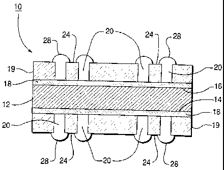
Fig. 1 is illustrative of a microelectronic package employing the
bonding layer of the present invention. The co-fired-ceramic on metal
3 0 structure 10 comprises a metal base 12 having first and second major
surfaces 14 and 16. A glass bonding layer 18 of the invention covers one or
both major surfaces 14 and 16. A multiple layer stack of laminated and
glass-ceramic/filler tape 19, having openings therein 20 for placing
semiconductor devices 24. The printed circuits and vias (not shown) in the
3 5 glass ceramic stack 19 are made from conductive metal powders such as
copper, silver, silver/palladium alloy, gold, alloys thereof and the like.
After co-firing the bonding glass-substrate core to the ceramic stack,
semiconductor devices 24 are assembled on the substrate by wire bonds 28
CA 02211533 1997-07-25
WO 96!23321 PCT/US96/003I5
9
or other means known to those skilled in the art, to electrically connect the
printed circuit stack to the semiconductor devices. The chips are then
sealed either by brazing metal lids (not shown) to the substrate, or by
dispensing an organic encapsulant (not shown) on the chip.
The invention will be further described in the following Examples, but
the invention is not meant to be limited to the details described therein.
Example 1
A nickel plated Cu/Mo/Cu (14/62/14) support substrate 0.020 inch in
thickness was prepared by screen printing a patterned layer of a bonding
1 0 glaze ink containing powder of the bonding glass No. 2, followed by firing
to
850oC in air to reflow and fuse the bonding glass layer to the substrate.
Six layers of green tape made using the forsterite-cordierite glass
described hereinabove, each green tape having a screen printed thick film
circuit pattern thereon made from silver inks, and punched via holes filled
1 5 with suitable silver-containing via inks, were aligned together and
laminated
at a pressure of 1500 psi at 90°C.
The green laminate was then pressed onto the glazed surface of the
support substrate and the assembly was fired in air to a peak temperature
of 900oC. A sintered glass-ceramic multilayer substrate integrally bonded
2 0 to the Cu/Mo/Cu support substrate was obtained.
The fired ceramic laminate was found to be well adhered to the
support substrate and had undergone no x, y shrinkage during the above
firing step, all of the firing shrinkage having occurred in the z direction.
Example 2
2 5 Following the procedure of Example 1, a bonding glaze ink was
substituted which contained a mixture of powdered bonding glass No. 1 and
bismuth oxide in a ratio by weight of 3:1.
Again, a composite multilayer ceramic structure on a Cu/Mo/Cu
support substrate was obtained that had undergone no x, y shrinkage
3 0 during the firing step.
Example 3
Six layers of green tape made using another dielectric glass having a
~ composition, in % by weight of magnesium oxide, 32.5%, barium oxide, 17%,
aluminum oxide, 7%, silicon oxide, 24%, boron oxide, 16%, zirconium dioxide,
3 5 2.5% and phosphorus pentoxide, 1%, each having screen printed thick film
circuit patterns made from silver inks thereon, and punched via holes filled
with a suitable silver-containing via ink, were aligned together and
laminated at a pressure of 1500 psi at 90oC.
CA 02211533 1997-07-25
WO 96/23321 PCTIUS96/00315
Separately, a support substrate of Kovar, 0.020 inch in thickness,
was prepared by screen printing a patterned layer of a bonding glaze ink
containing the glass No. 1, followed by firing to 850oC in air to reflow and
fuse the bonding glass layer to the substrate. The green laminate as above
5 was then pressed onto the glazed surface of the support substrate and the
assembly was fired in air to a peak temperature of 900oC.
A sintered glass-ceramic multilayer substrate, integrally bonded to
the Kovar support substrate, was obtained.
The green tape laminate was found to be well adhered to the Kovar
1 0 support substrate, and had undergone no x, y shrinkage during the firing
step. Thus all of the firing shrinkage occurred in the z direction.
Although the present invention has been described in terms of
specific embodiments, one skilled in the art can readily substitute other
resins and materials used to make green tape and conductor inks, other
1 5 metal substrates and other bonding glasses providing they meet the
criteria
set forth above. Thus the invention is meant only to be limited by the
appended claims.