Note : Les descriptions sont présentées dans la langue officielle dans laquelle elles ont été soumises.
CA 02229890 l998-02-l8
W O 97/08887 PCTICA96/00515
APPARATUS AND METHOD FOR ADRESSING CELLS OF INTEREST IN A SOLID STATE SENSOR
FIELD OF THE INVENTION
The present invention is concerned with an addressing
and extracting apparatus for addressing sensing cells of
interest in a solid state sensor, and extracting thereof
resulting signals, and with a method thereof. This
invention relates to solid state image sensing.
BACKGROUND OF THE INVENTION
Conventionally, solid state sensors use a simple
pixel architecture with a single selection line in one
direction and a unique analog data bus on the opposite
direction. Thus, when a particular selection line of a
conventional sensor is activated, every pixel on the
selected line puts its resulting signal on the data bus
which is routed out using an extraction module, generally
implemented by a shift register. Also, some versions of
large image sensors have multiple outputs in order to
reduce the time required to extract the entire resulting
information from the sensor.
Known in the art, there is the publication entitled
"High resolution smart image sensor with integrated
parallel analog processing for multi resolution edge
extraction", pllhl;~:h~-l in Robotics and Autonomous Systems,
11 (1993) 231-242, by Tremblay, M., Laurendeau, D. and
Poussart D. In this publication there is described a
conceptual and extremely simplified high resolution smart
image sensor with integrated parallel analog processing.
A drawback with the system described in this publication
is that only basic principles are given to the reader and
CA 02229890 l998-02-l8
essential elements are missing so that the reader cannot
built an actual operating prorotype.
Also known in the art is the US patent no
5,070,414 of Teruo Tsutsumi granted on December 3, 1991.
In this patent, there is described a method and apparatus
for reading image information formed on material. With
this method and apparatus, analog multiplexers are
responsive to clock pulses from a timing generator to
select output signals from buffer amplifiers in a
predetermined sequence, thus producing a serial signal. A
drawback with the above described method and apparatus is
that the information extracted is only available in a
serial signal.
Also known in the art, there are the following us
patents 4,541,015; 4,597,012; 4,644,406; 4,985,619;
5.016,108; 5,036,396; 5,051,831; 5,070,414; 5,157,422;
5,253,071; 5,288,988; et 5,317,423. None of the above
mentioned patents or publication, described the necessary
means allowing parallel extraction of resulting signals
from a group of pixels located on a dedicated region of
interest.
It is thus an object of the present invention to
provide an addressing and extraction architecture for a
solid state sensor in order to allow parallel extraction
of resulting signals from a group of pixels located on a
dedicated region of interest, in a simple and efficient
manner.
SUMMARY OF THE INVENTION
According to the present invention, there is
provided an addressing and extracting apparatus for
addressing sensing cells of interest in a solid state
sensor, and extracting thereof resulting signals, the
solid state sensor inc~uding a pluralitv of sensing cells,
each of the sensing cells having a sensitive unit for
A~ S~
CA 02229890 1998-02-18
receiving a physical phenomenon and producing a resulting
signal representative of an intensity of the physical
phenomenon received by the sensitive unit, and a first
sensing controllable switch having a ~irst terminal for
receiving the resulting signal from the sensitive unit, a
second terminal for delivering upon activation of the
switch the resulting signal, and a control gate; the
apparatus comprising:
a first selecting line connected to a first
sensing array of n sensitive units by the control gates of
their associated first sensing controllable switches;
a first sensing activating means for activating
the first selecting line;
n sensing data lines connected respectively to
the n sensitive units of the first array by the second
terminals of their associated first sensing controllable
switches so that, in operation, each of the sensing data
lines receives the corresponding resulting signal when the
first selecting line is activated; and
a controller for controlling and synchronizing
operation of each of the sensing activating means,
whereby, upon activation of the activating means, the
sensing cells of interest are addressed;
the addressing and extracting apparatus being~5 characterized in that it further comprises:
a first parallel analog multiplexer comprising:
a first bidimensional extracting array of
first controllable extracting switches, having a first
dimension of n columns by a second dimension of k rows, k
being a positive integer representative of the amount of
the sensing cells of interest, each of the first
controllable extracting switches having a first terminal,
a second terminal and a control gate, each one of the n
sensing data lines being connected to a corresponding one
of the n columns of first controllable extracting switches
by first terminals thereof;
AMENDE~SHE~
CA 02229890 1998-02-18
n first extracting selecting lines each
connected to the control gat~s of a group of the first
controllable extracting switches, the first controllable
extracting switches of each group forming an axis
transversal to the columns and rows of the first
bidimensional extracting array; and
k first extracting data lines each connected
to a corresponding one of the k rows of first controllable
extracting switches by second terminals thereof;
a first extracting activating means for
individually activating the first extracting selecting
lines, according to a given sequence; and
the addressing and extracting apparatus being also
characterized in that the controller being also for
controlling and synchronizing operation of each o~ the
extracting activating means for individually activating
the extracting selecting lines whereby signals resulting
from the sensing cells of interest are extracted via the
first extracting data lines.
According to the present invention, there is also
provided a method for addressing sensing cells of interest
in a solid state sensor, and extracting thereof resulting
signals after a previous step of (a) receiving a physical
phenomenon by means o~ a solid state sensor including a
plurality of sensing cells, each of the sensing cells
having a sensitive unit for receiving a physical
phenomenon and producing a resulting signal representative
of an intensity o~ the physical phenomenon received by the
sensitive unit, and a first sensing controllable switch
having a first terminal for receiving the resulting signal
from the sensitive unit, a second terminal for delivering
upon activation of the switch the resulting signal, and a
control gate; the method comprising steps of:
(b) providing a first selecting line connected to
a first sensing arrav of n of the sensitive units by the
control gates of their associated first sensing
AMENDED SHEET
CA 02229890 1998-02-18
controllable switches;
(c) activating the first selecting linei
(d) providing n sensing data lines connected
respectively to the n sensitive units of the array by the
second terminals of their associated first sensing
controllable switches so that, in operation, each of the
sensing data lines receives the corresponding resulting
signal when the first selecting line is activated; and
(e) controlling and synchronizing operation of
lo step (c), whereby, upon activation of step (c), the
sensing cells of interest are addressed;
the method being characterized in that it further
comprises a step of (f) providing a first parallel analog
multiplexer comprising:
a first bidimensional extracting array of
first controllable extracting switches, having a first
dimension o~ n columns by a second dimension of k rows, k
being a positive integer representative of the amount of
the sensing cells of interest, each of the first
controllable extracting switches having a ~irst terminal,
a second terminal and a control gate, each one of the n
sensing data lines being connected to a corresponding one
of the n columns of first controllable extracting switches
by first terminals thereof;
n first extracting selecting lines each
connected to the control gates of a group of the first
controllable extracting switches, the first controllable
extracting switches of each group forming an axis
transversal to the columns and rows of the first
bidimensional extracting array; and
k first extracting data lines each connected
to a corresponding one of the k rows of first controllable
extracting switches by second terminals thereof;
(g) individually activating the first extracting
selecting lines according to a given se~uence; and
(h) controlling and synchronizing operation of
- AMENDEDS~E~
CA 02229890 1998-02-18
5a
step (g), whereby signals resulting from the sensing cells
of interest are extracted via the first extracting data
lines.
BRIEF DESCRIPTION OF THE DRAWING
Fig. 1 is a conceptual schematic block diagram of
an
//
,~ / /
,//
/
~'j /
h,~ 'iGt5SHF,~
CA 02229890 1998-02-18
W O 97/08887 PCT/CA96/00515
apparatus according to the present invention;
Fig. 2 is a circuit diagram of a part of the
apparatus shown in figure 1;
Fig. 3 is a schematic block diagram of an apparatus
according to the present invention;
Fig. 4 is a circuit diagram of a part of the
apparatus shown in figure 3;
Fig. 5 is a circuit diagram of a another part of the
apparatus shown in figure 3;
Fig. 6 is a schematic diagram partially in block and
partially in circuit of an embodiment of the apparatus
schematically shown in figure 3;
Fig. 7 is a schematic block diagram of another
apparatus according to the present invention;
Fig. 8 is a schematic diagram partially in block and
partially in circuit of an embodiment of the apparatus
schematically shown in figure 7;
Fig. 9 is a schematic block diagram of another
apparatus according to the present invention;
Fig. 10 is a circuit diagram of a part of the
apparatus shown in figure 9; and
Fig. 11 is an algorithm illustrating the steps
performed by the controller shown in figures 3, 6, 7, 8
and 9.
DETAILED DESCRIPTION OF THE DRAWINGS
The present description is in the context of
artificial vision but the present invention can be applied
to physical phenomena other than the ones in the context
o~ artificial vision. An object of artificial vision is to
reconstruct a scene cont~;n;ng explicit and significant
objects which can be further recogn;~ed and processed. The
necessary flow of data constitutes the principal
limitation of artificial vision since it exceeds
processing capacities of conventional digital systems. In
CA 02229890 1998-02-18
W O 97/08887 PCT/CA96/00515
fact, processing of a single image normally requires the
reading and writing of tens of millions of bytes, either
into memory or onto an external medium. Such processing
may last up to several minutes. Therefore, improvements
~ 5 in artificial vision dictate the development of more
effective systems.
The system according to the present invention is
called Multiports Array of photo-Receptors system or MAR
system. In the following description, we will sometimes
refer to MAR system. The MAR system con~ers a processing
power equivalent to several billions of operations per
second when coupled to an image processing analog unit or
filtering circuit. The MAR system will be described below
in a simple manner.
The MAR sensor is a CMOS integrated circuit
comprising more than one million transistors. It is
specially dedicated to artificial vision. This circuit is
normally provided with tens of analog outputs. A data
extracting method supported by the architecture per~orms
a data structuring at the outputs of the system so that a
direct data processing is already achieved at the output
o~ the MAR system. Consequently, with the MAR system,
millions of memory readings and writings which are
normally required by a conventional image processing
digital system for performing the same task, are not
required anymore.
An advantage of the MAR system is that each single
data, pixel or picture element of its pixel matrix, which
corresponds to the intensity of each point of the image,
can be read several times without being destroyed. Most
optical sensors available on the market use destructive
reading which means that once data is read it cannot be
read again. Hence, the MAR system allows multiple
readings of each of its pixels.
In fact, when the intensity value of a selected image
point or pixel is read, the MAR system provides in
CA 02229890 1998-02-18
WO 97/08887 PCT/CA96/00515
parallel intensity values of the selected pixel with tens
of pixels surrounding the selected pixel. All of these
pixels are called the pixels of interest. It is then
possible to perform image processing or image filtering at
the reading instant. Then the image is captured by means
of an appropriate module and transferred into a memory.
Subsequently, digital vision systems perform numerous
memory access in order to obtain information from
neighbouring pixels and finally achieve processing of the
lo selected pixel.
Each pixel is selected by sweeping the pixel matrix
line by line. For example, 262,144 selections are
performed for a sensor having a 512 by 512 pixel matrix.
For each selected pixel, the parallel data extraction is
realized by the Parallel Analog Multiplexer or PAM. In the
following description, we will sometimes refer to PAM.
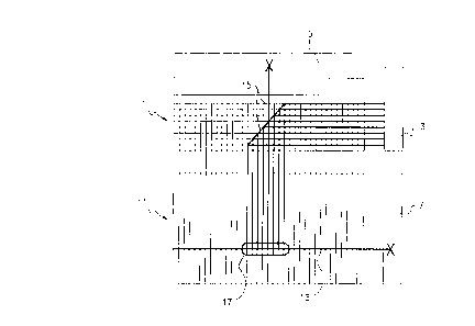
This PAM 1 is illustrated in figure 1. Operating as an
intersection manager, it directs data from the selected
line 13 of the pixel matrix 11 to the correct outputs 3 of
the system.
To move the position of the selected pixel in the
pixel matrix 11, shift registers 9 such as the ones shown
in figure 2 are used. By referring to figures 1 and 2,
the internal shifting structure operation of this type of
register will be explained. The activating means 5 and 7
each comprises shift registers 9 as shown in figure 2. The
position of the X represents the selected element or the
line that is activated. The selected shift register X of
the activating means 7 corresponds to a selecting line 13
of the pixel matrix 11. The selected shift register X of
the activating means 5 corresponds to the selecting
diagonal 15 of the PAM 1.
The operation of the shift registers g only allows
three simple actions which are no displacement, a
displacement of one position to the right, and a
displacement of one position to the left. For example, in
CA 02229890 1998-02-18
W O 97/08887 PCT/CA96/00515
order to sweep all of the lines of the pixel matrix 11,
one has to perform as many displacements of one position
as the number of lines in the matrix 11. This principle
is applicable for each of the activating means 5 and 7.
When the M~R system is swept, the pixels of interest
can be displaced by one pixel horizontally or vertically.
In the particular case of figure 1, there are four
possible displacements of the pixels of interest. A first
possible displacement is a displacement to the left of the
pixels of interest 17 by displacing to the left the
diagonal 15 selected by activating means 5 and keeping the
line 13 selected by the activating means 7 unchanged. The
active shift register of the activating means 5 is moved
to the left whereas the active shift register of the
activating means 7 is maintained. The new pixels of
interest which are centred on a new position of the
selecting diagonal are then directed to the outputs 3 of
the PAM 1.
A second possible displacement is a displacement to
the right of the pixels of interest by displacing to the
right the diagonal 15 selected by activating means 5 and
keeping the line 13 selected by the activating means 7
unchanged. The active shift register of the activating
means 5 is moved to the right whereas the active shift
register of the activating means 7 is maintained. The new
pixels of interest which are centred on a new position of
the selecting diagonal are then directed to the outputs 3
of the PAM 1.
A third possible displacement is an upward
displacement of the pixels of interest 17 by displacing
upwardly the line 13 selected by activating means 7 and
keeping the column or diagonal 15 selected by the
activating means 5 unchanged. The active shift register of
the activating means 7 is moved upwardly whereas the
active shift register of the activating means 5 is
maintained. The new pixels of interest which are centred
CA 02229890 1998-02-18
W O 97/08887 PCT/CA96/00515
on a new position of the selecting line 13 are then
directed to the outputs 3 of the PAM 1.
The fourth possible displacement is an downward
displacement of the pixels of interest 17 by displacing
downwardly the line 13 selected by activating means 7 and
keeping the column or diagonal 15 selected by the
activating means 5 unchanged. The active shift register of
the activating means 7 is moved downwardly whereas the
active shift register of the activating means 5 is
maintained. The new pixels of interest which are centred
on a new position of the selecting line 13 are then
directed to the outputs 3 of the PAM.
Referring now to figure 3, there is proposed a
preferred embodiment of the present invention for a
Cartesian topology architecture where two parallel analog
multiplexers or PAMs 26 and 64 are used. one PAM 26 or 64
is used for each ~;men~ion of the pixel matrix. A person
skilled in the art will understand that ~or an application
to a hexagonal topology architecture, some modifications
are necessary for adapting the sweeping management of the
pixel matrix so that the new spatial constraints o~ this
topology are taken into consideration. But the basic
principles applied to the Cartesian topology architecture
can also be applied to a hexagonal topology architecture.
25The M~R system can be defined as a pixel matrix from
which data extraction is rendered possible via parallel
analog multiplexers or PAMs which are controlled by their
associated shift registers. Figure 3 shows a global view
of the integrated circuit of the MAR system applied to a
Cartesian topology architecture. The selected pixel is
the one at the intersection of the selected line and
column in the pixel matrix. The selection is performed by
the shi~t registers of the activating means 18 and 60.
Referring now to figures 3 to 6, there are shown two
parallel analog multiplexers or PAMs 26 and 64 by which it
is possible to obtain a multiport access of the sensitive
CA 02229890 1998-02-18
WO 97/08887 PCT/CA96/00515
units or photoreceptors 6 of the solid state sensor 2. The
solid state sensor 2 covers N x M sensitive units or
pixels 6. Each sensitive unit 6 has a multiport addressing
architecture with axis selection lines 16 and 58 and
output sensing data lines 20 and 62. The addressing and
extraction architecture shown in figures 3 to 6 has two
axis systems. The first PAM 26 is used for a first axis
system whereas the second PAM 64 is use for the second
axis system.
The multiple extracting data lines 36 and 72 supply
output signals to an analog computing module (not shown)
for computing, in real time, these output signals which
are a filtered representation of the current image
detected by the sensing cells or pixels of interest 42.
There is shown in figure 6 an example of a sc~nning
device having six sensing cells 4. The invention can be
generalized for both Cartesian or hexagonal regular
tessellation. For each type of tessellation, there can be
defined a multiport access photoreceptor sensor (MAR),
having various number of axis systems.
Thus, the present architecture gives access,
simultaneously, to a set of individual analog signals
which are extracted from a given area on the solid state
sensor 2. The figures 3 to 6 show a two-axis system but
the present invention can be embodied with a plurality of
axis systems.
The addressing and extracting apparatus is for
addressing sensing cells of interest 42 in the solid state
sensor 2, and extracting thereof resulting signals. The
apparatus comprises a solid state sensor 2 including a
plurality of sensing cells 4. Each of the sensing cells 4
has a sensitive unit 6 for receiving a physical phenomenon
and producing a resulting signal representative of an
intensity of the physical phenomenon received by the
sensitive unit 6. In the present case, the phenomenon
received is light. It has also a controllable switch 8
CA 02229890 1998-02-18
W O 97/08887 PCT/CA96/OOS15
having a first terminal 10 for receiving the resulting
signal from the sensitive unit 6, a second terminal 12 for
delivering upon activation of the switch the resulting
signal, and a control gate 14.
At least one first sensing selecting line 16 is
provided. Each selecting line 16 is connected to a
sensing array 17 of n of the sensitive units 6 by the
control gates 14 of their associated first sensing
controllable switches 8. A first sensing activating means
lo 18 such as shift registers is provided ~or individually
activating the first sensing selecting lines 16.
N sensing data lines 20 are connected respectively to
the n sensitive units 6 of each array by the second
terminals 12 o~ their associated controllable switches 8
so that, in operation, each of the sensing data lines 20
receives the corresponding resulting signal when one of
the first sensing selecting lines 16 is activated.
A parallel analog multiplexer 26 is provided. It
comprises a first bi~ime~ional extracting array of con-
trollable switches 24. The first bi~;m~n~ional extractingarray has a first ~im~ion of n columns by a second
~;men~ion of k rows. R is a positive integer
representative of the amount of the sensing cells of
interest 42. Each of the controllable switches 24 has a
first terminal 28, a second terminal 30 and a control
gate 32. Each one of the n sensing data lines 20 is
connected to a corresponding one of the n columns of
controllable switches 24 by first terminals 28 thereof.
N first extracting selecting lines 34 are provided.
Each of the N first extracting selecting lines 34 is
connected to the control gates 32 of a group of the
controllable switches 24. The controllable switches 24 of
each group form an axis transversal to the columns and
rows of the first bi~ime~sional extracting array. In the
present description, we use the expressions parallel,
transversal, columns and rows to describe the
CA 02229890 1998-02-18
W 097/08887 PCT/CA96/00515
configuration of certain elements shown in the figures
because it is easier to explain the invention with the use
~ of these expressions but it should be understood that
these elements are not necessarily in practice physically
positioned in columns or rows, or transversal or parallel.
First extracting data lines 36 are provided. There
are k of them and are each connected to a corresponding
one of the k rows of controllable switches 24 by second
terminals 30 thereof. An extracting activating means 38
such as shift registers is provided for individually
activating the first extracting selecting lines 34
according to a given sequence. A controller 40 is provided
for controlling and synchronizing operation of the
activating means 18 and 38 , whereby, upon activation of
the activating means 18 and 38, the sensing cells of
interest 42 are addressed, and the corresponding resulting
signals are extracted via the first extracting data lines
36.
Several first sensing selecting lines 16 are
provided. Each of the first sensing selecting lines 16 is
connected to one of the first sensing arrays 17 of n
sensitive units 6 by the control gates 14 of their
associated controllable switches 8. The first sensing
arrays 17 of sensitive units 6 are parallel. The sensing
activating means 18 is for individually activating the
first sensing selecting lines 16 according to a given
sequence. The n sensing data lines 20 are each connected
to one of the n sensitive units 6 of each array 17 by the
second terminals 12 of their associated controllable
switch 8.
Each of the sensing cells 4 further comprises a
controllable switch 50 having a first terminal 52 for
receiving the resulting signal from the corresponding
sensitive unit 6, a second term; n;ll 54 for delivering upon
activation of the switch 50 the resulting signal, and a
control gate 56. Second sensing selecting lines 58 are
CA 02229890 1998-02-18
W O 97/08887 PCT/CA96/00515
14
also provided. Each of the second sensing selecting lines
58 is connected to a second sensing array 57 of m
sensitive units 6 by the control gates 56 of their
associated controllable switches 50. The second sensing
arrays 57 of sensitive units 6 are parallel and are also
transversal to the first sensing arrays 17.
A second sensing activating means 60 such as shift
registers is provided for individually activating the
second sensing selecting lines 58 according to a given
lo sequence. M sensing data lines 62 are provided and are
each connected to one of the m sensitive units 6 of each
second sensing array by the second t~rm; n~l s 54 of their
associated controllable switches 50.
A parallel analog multiplexer 64 is provided. It
comprises a second bi~imen~ional extracting array of
controllable switches 66. The second bi~imensional
extracting array has a first ~im~n~cion of m columns by a
second ~imen~ion of k rows. Each of the controllable
switches 66 is similar to the one shown in figure 5. Each
controllable switch 66 has a first terminal, a second
terminal and a control gate. Each one of the m sensing
data lines 62 is connected to a corresponding one of the
m columns of controllable switches 66 by the first
terminals thereof.
M second extracting selecting lines 70 are provided.
Each of the m second extracting selecting lines 70 is
connected to the control gates of a group of the
controllable switches 66. The controllable switches 66 of
each group form an axis transversal to the columns and
rows of the second bi~imen~ional extracting array.
Second extracting data lines 72 are provided and
there are k of them. Each of the second extracting data
lines 72 is connected to a correspo~i ng one of the k rows
of controllable switches 66 by the second terminals
thereof. A second extracting activating means 74 such as
shift registers is provided for individually activating
CA 02229890 l998-02-l8
W O 97/08887 PCT/C~96/00515
the second extracting selecting lines 70 according to a
given sequence.
Noticeably, for a simple topology like the Cartesian
topology, several simplifications can be made at the level
of activating means. An activating means can
simultaneously select one line or column in the solid
state sensor and one extracting selecting line of a
parallel analog multiplexer or PAM.
Referring now to figures 7 and 8, there is shown an
embodiment of the apparatus shown in figures 3 to 6 where
simplifications are made at the level of the activating
means. In this embo~;m~nt, the first and second extracting
activating means 38 and 74 shown in figures 3 and 6 are
respectively carried out by the second and first sensing
activating means 60 and 18.
The second sensing selecting lines 58 are
respectively connected to the first extracting selecting
lines 34 so that the selecting lines 34 and 58 are
simultaneously activated by the second sensing activating
means 60. The first sensing selecting lines 16 are
respectively connected to the second extracting selecting
lines 70 so that the selecting lines 16 and 70 are
simultaneously activated by the first sensing activating
means 18. In the apparatus shown in figures 6 and 8, k=2.
Referring now to figures 9 and 10 there is shown
another embodiment of the apparatus wherein each of the
sensing cells 4 ~urther comprising an additional
controllable switch 90 having a first terminal 92 for
receiving the resulting signal from the corresponding
sensitive unit 6, a second term; n~l 94 for delivering upon
activation of the switch 90 the resulting signal, and a
control gate 96. The apparatus further comprising third
sensing selecting lines 98 each connected to a third
sensing array 97 of p sensitive units 6 by the control
gates 96 of their associated controllable switches 90. The
third sensing arrays 97 of sensitive units 6 are parallel
CA 02229890 1998-02-18
W O 97/08887 PCT/CA96/0051~
and are also transversal to the first and second sensing
arrays of sensitive units ~.
A third sensing activating means loo is provided for
individually activating the third sensing selecting lines
98 according to a given sequence. P sensing data lines 102
are provided. Each of the P sensing data lines 102 are
connected to one of the p sensitive units 6 of each third
sensing array 97 by the second terminals 94 of their
associated controllable switches go.
A third parallel analog multiplexer or PAM 104 is
provided. It comprises a third bi~;men.cional extracting
array of controllable switches which is similar to ~irst
and second b;~imen~ional extracting arrays shown in
figures 6 and 8. The third bi~ n~ ional extracting array
has a first ~;me~ion of p columns by a second dimension
of k rows. Each of the controllable switches of the third
bidimensional extracting array has a first terminal, a
second terminal and a control gate. Each one of the p
sensing data lines 102 are connected to a corresponding
one of the p columns of the controllable switches of the
third bi~;mensional extracting array by the first
termin~-s thereof. P third extracting selecting lines 106
each connected to the control gates of a group of the
third controllable extracting switches. The third
Z5 controllable extracting switches of each group form an
axis transversal to the columns and rows of the third
bi~im~n~ional extracting array.
The parallel analog multiplexer 104 is similar to PAM
26 or 64. It comprises k third extracting data lines 108
each connected to a corresponding one of the k rows of
third controllable extracting switches by a second
t~rmin~ls thereof. A third extracting activating means llo
is also provided for individually activating the third
extracting selecting lines 106 according to a given
sequence. Preferably, m, n and p are the same number.
Referring now to figure 11, there is illustrated an
CA 02229890 1998-02-18
WO 97/08887 PCT/CA96/00515
algorithm of the steps performed by the controller shown
in figures 3, 6, 7, 8 and 9. Several sc~nn;ng routines
are performed until the whole solid state sensor is
covered. During a single sc~nn;ng routine, for each PAM
one sensing selecting line and one extracting selecting
line are activated, and the extracting data lines of each
PAM are read. During the successive sc~nn;ng routines at
least one of the selecting lines is changed by shifting a
shift register of its associated activating means.
Although the present invention has been explained
hereinafter by way of preferred embodiments thereof, it
should be pointed out that any modifications to these
preferred embodiments, within the scope of the appended
claims, are not deemed to change nor alter the nature and
scope of the present invention.