Note : Les descriptions sont présentées dans la langue officielle dans laquelle elles ont été soumises.
CA 02232760 1998-03-19
H6504, 6-300
N-WAY RF POWER COMBINER IVIDER
This invention relates to an of RF power combiner/divider circuits for use in
combining
or dividing RF signals.
Combiner/dividers are known for combining or dividing (splitting) electrical
signals. A
RF signal generator may produce a radio frequency signal at a low power level
and it may be
desired that the signal be boosted in power to a much higher level. It is
common to divide the
RF signal and apply the divided signals to several paths each of which
includes a power
amplifier for increasing the amplitude of the signal. Conversely, RF signals
which have been
amplified may be combined and supplied to a RF load.
Combiner/dividers capable of performing these functions are disclosed in the
1o specification of U.S. patent No. 4,163,955 and discloses a N-way power
combiner/divider known
as the Gysel combiner/divider. An example of a Gysel combiner may take the
form of a
two-way hybrid ring combiner. Such a combiner is disclosed in Figs. 1 and 2
herein. This
combiner, includes six 90 ° phase shifting sections, two coherent RF
power sources, and two
isolation resistors. Two RF signals are respectfully applied to two input
ports to cause RF signals
1s to propagate through the phase shifting sections and combine at a common
port. The signals
arrive at the common port with the same phase shift of 90°.
The Gysel type combiner/divider structures shown in Figs.1 and 2 employ six
90° phase
shifting sections or branches. A modified form of these Gysel structures is
shown in Figs. 3 and
4 including only four phase shifting sections to provide a simpler structure
and which exhibits
2o a greater frequency band. This structure, includes one phase shifting
section that shifts the phase
by -90 ° instead of shifting the phase by +90 ° as in ~e case of
the other three phase shifting
branches. This structure is simpler than as shown in Figs.1 and 2 in that it
also has only a single
isolation resistor. A disadvantage of the modified Gyseh device of Figs. 3 and
4 is the
non-symmetry of its structure. 1?ue to the frequency dependent amplitude
response of the
2s reversed transmission line (the -90° phase shifting branch), the
power sources need to provide
different power levels for an optimal performance.
The present invention includes an N-way RF power combiner/divider comprising:
a common output/input port;
N input/output ports;
so N isolation ports;
a 90° phase shifting transmission line interconnecting each of said N
input/output ports with said common port; and,
1
CA 02232760 1998-03-19
H6504, 6-300
N transmission line balun transformers, each said transformer interconnecting
a
said input/output port with one of said N isolation ports.
The invention also includes an N-way RF power combiner/divider comprising:
a common output/input port;
N input/output ports;
N isolation ports;
a 90 ° phase shifter interconnecting each of said N input/output ports
with
said common port; and,
N two-way power splitters each having a +90° phase shift output
and a
to -90 ° phase shift output with the +90 ° phase shift output of
one sputter being connected
in common with the -90 ° phase shift output of another of said
splitters and with one of
said N isolation ports.
An object of the invention is to provide an improved combiner/divider circuit
exhibiting greater symmetry and increased frequency range. Advantageously,
there is
15 provided a N-way RF power combiner/divider including a common output/input
port
and a plurality of N input/output ports and a plurality of N isolation ports.
A 90°
phase shifting transmission line interconnects each of the N input/output
ports with the
common port. N transmission line balun transformers are provided. Each
transformer
interconnects one of the input/output ports with one of the isolation ports.
2o Conveniently, there is provided a N-way RF power combiner/divider including
a common output/input port and a plurality of N input/output ports and a
plurality
of N isolation ports. A 90 ° phase shifting transmission line
interconnects each of the N
input/output ports with the common port. N two-way power splitters are
provided.
Each splitter has a +90 ° phase shift output and a -90 ° phase
shift output with the +90 °
2s phase shift output of one splitter being connected in common with the -90
° phase shift
output of another splitter. This common connection is also common to one of
the
isolation ports.
The invention will now be described, by way of example, with reference to the
accompanying drawings;
z
CA 02232760 1998-03-19
H6504, 6-300
Fig. 1 is a schematic-block diagram illustration of a prior art combiner/
divider
operating as a combiner;
Fig. 2 is a schematic illustration of a transmission line implementation of
the
combiner/divider of Fig. 1 but illustrated as a divider;
Fig. 3 is a schematic-block diagram illustration of a prior art modification
of the
combiner/ divider in Fig. 1;
Fig. 4 is a circuit diagram illustration of a transmission line implementation
of the
prior art circuit of Fig. 3;
Fig. 5 is a schematic-block diagram illustration of one embodiment of the
present
io invention;
Fig. 6 is a circuit diagram illustrating a transmission line implementation of
the
embodiment of the invention shown in Fig. 5;
Fig. 7 is a schematic-block diagram illustration of a second embodiment of the
present invention;
is Fig. 8 is a circuit diagram illustration of a transmission line
implementation of the
embodiment shown in Fig. 7; and
Fig. 9 is a schematic circuit illustration of a transmission line
implementation of
a third embodiment of the present invention.
Before describing the preferred embodiments of Figs. 5-9, reference is first
made to a
2o discussion of the prior art illustrated in Figs. 1-4.
Fig.1 illustrates a prior art combiner/divider 10 illustrated as a combiner.
This
is a hybrid ring that is sometimes known as a Gysel combiner and is disclosed
in the
specificaiton of U.S. Patent No. 4,163,955. Fig. 1 shows the combiner
illustrated as a
two-way combiner having six 90 ° phase shifting sections arranged in a
hexagon. The
2s combiner includes two input/output ports 12 and 14, a common output/input
port 16,
and a pair of isolation ports 18 and 20. A RF power source 22 is connected to
the
input/output port 12 which serves as an input port for a combiner
implementation.
S~~'ly. a RF power source 24 is connected to the input/output port 14 serving
as an
input port. The common port 16 serves as an output port and is connected to
ground
so by way of a common load resistor 26. Isolation ports 18 and 20 are
connected to ground
3
CA 02232760 1998-03-19
H6504, 6-300
by way of isolation loads 30 and 32. The six branches of the combiner each
include a
+90 ° phase shifter. These branches include phase shifters 40, 42, 44,
46, 48, and 50, as
shown.
The two RF power signals from sources 22 and 24 are coherent RF power sources
s and provide two signals which are applied to the input ports 12 and 14.
These signals
propagate through the phase shifters and combine at the output port. As seen,
these
signals arrive at the output port 16 with the same phase shift of +90 °
. Also, the
propagation path of both signals from sources 22 and 24 to the isolation loads
30 and 32
shows that the signals will arrive at these ports out of phase. They subtract
and since
io they were initially of equal amplitude and phase they entirely eliminate
each other.
The two RF power sources 22 and 24 are isolated from each other. Thus, the RF
signal from source 22 does not appear at input port 14 for source 24 and vice
versa. This
happens because the RF input signal from source 22 splits by two and
propagates two
opposite ways to reach input port 14. Also, the two branches of the signal
propagating
i5 from source 24 arrive at port 12 out of phase and eliminate each other
which results an
entire isolation. This is an ideal case of frequency independent combiner
structure. The
actual structure takes the form as shown in Fig. 2.
Fig. 2 illustrates the hybrid ring of Fig.1 as a divider and not as a
combiner. Like
components in Figs. 1 and 2 are identified with like character references and
only the
2o differences will be described. The divider of Fig. 2 include ports 12 and
14 acting as
output ports instead of input ports and a common port 16 which serves in this
case as
an input port. Isolation ports 18 and 20 are connected through isolation
resistors 30 and
32 to ground, as in the case of Fig.1. However, the input sources 22 and 24 of
Fig.1 are
replaced in Fig. 2 with load resistors 23 and 25. The common port 16 serves as
an input
25 port and is connected by way of resistor 27 to a single RF signal source
29. The divider
or splitter structure in Fig. 2 is a transmission line implementation of the
hybrid ring
structure and as such includes six transmission line sections in place of the
six phase
shifting sections of Fig.1. These are transmission line sections 41, 43, 45,
47, 49, and 51.
Each may include a microstrip structure including a pair of conductor strips
spaced
4
CA 02232760 1998-03-19
H6504, 6-300
from each other by an intermediate dielectric insulator. The inner conductor
strips of
these transmission lines are connected to electrical ground.
Each transmission line section has a length of 1/4 wavelength to provide a
phase
shift of +90 ° . This phase shift, however, takes place at only one
frequency and the
frequency range of such a hybrid structure is ten percent when the input VSWR
is less
than or equal to 1.1 to 1.
Fig. 3 illustrates a prior art modified hybrid ring combiner which has a
greater
frequency band than that of the two-way combiner shown in Fig. 1. As a two-way
combiner, the combiner 100 of Fig. 3 includes two input ports 112 and 114 and
a
io common output port 116 and a single isolation port 118. The common port is
connected
to ground by way of a load resistor 126 and the isolation port 118 is
connected to ground
by way of a single isolation load 130. The four phase shifting sections
include phase
shifters 140,142,146, and 148. Thus, only four phase shifters are employed
instead of
six as in Fig.1. The significant difference is that one of the phase shifters
provides a -90°
i5 phase shift instead of a +90 ° phase shift. It operates in the same
fashion as that of the
version in Fig. 1 but requires a simpler structure in the form of a square
instead of a
hexagon and employs only four phase shifters.
Fig. 4 illustrates a transmission line implementation of Fig. 3 as a combiner.
This
combiner 110 includes transmission lines in place of the phase shifters of
Fig. 3. This
2o includes transmission lines 141,143,147, and 149 in place of phase shifters
140,142,146,
and 148 respectfully of Fig. 3. It is to be noted, however, that transmission
line 147 has
its ends reversed connecting source 124 to ground instead of to the isolation
port 118.
This makes the transmission line 147 operate as a 180° phase shifter in
addition to the
90° phase shift that is provided by its 1/4 wavelength (each
transmission line has a
25 length of 1/4 wavelength). Therefore, the total phase shift provided by
transmission
line 147 is 270 ° (or -90 ° ). The difference from the hexagon
structure of Figs. 1 and 2
discussed hereinbefore is that the 180 ° phase shift works for all
frequencies the same.
It is not frequency dependent. Therefore, the bandwidth of this combiner is
greater than
that of versions in Figs.1 and 2. A disadvantage of the combiner of Figs. 3
and 4 is the
3o non-symmetry of its structure. Due to the frequency dependent amplitude
response of
5
CA 02232760 1998-03-19
H6504, 6-300
such a reversed transmission line, the power sources have to provide different
power
for optimal performance.
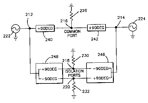
Fig. 5 which illustrates an embodiment of the present invention configured as
a
combiner. This is a special case that is presented as a two-way combiner (a
more general
s case of a N-way combiner is illustrated herein at Figs. 7 and 8). The two-
way combiner
of Fig. 5 includes a pair of input ports 212 and 214, a common output port 216
and a pair
of isolation ports 218 and 220. Input ports 212 and 214 receive RF power
signals from
RF sources 222 and 224. The common port 216 is connected to ground by way of a
load
resistor 226. Isolation ports 218 and 220 are connected to ground by way of
isolation
io loads 230 and 232. Input port 212 is connected to the common port 216 by
way of a +90 °
phase shifter 240. Also, input port 214 is connected to the common port 216 by
means
of a +90 ° phase shifter 242.
Input port 212 is connected to the isolation ports 218 and 220 by means of a
two-way power splitter 248. Power splitter 248 has a +90 ° phase shift
output connected
15 to isolation port 218 and a -90 ° phase shift output connected to
isolation port 220.
Similarly, input port 214 is connected to the isolation ports 218 and 220 by
means of a
two-way power splitter 246. This power splitter has a -90 ° output
connected to the
isolation port 218 and a +90 ° output connected to the isolation port
220. These two-way
power sputters 246 and 248 may be referred to as balun transformers which
equally
2o distribute the input signals between the two isolation loads. This makes
the structure
of the combiner symmetrical and increases the working frequency range.
Fig. 6 is a circuit diagram illustrating a transmission line implementation of
the
embodiment shown in Fig. 5. In this implementation, the +90 ° phase
shifters 240 and
242 are replaced with 1/4 length transmission lines 241 and 243. Also, the two-
way
2s power splitters 246 and 248 of Fig. 5 are replaced by balun transformers
247 and 249.
Note that the ends of the balun transformers are connected so as to provide
the phase
relationships as illustrated in Fig. 5.
Figs. 7 and 8 illustrate a general version of the invention as a N-way power
combiner. In Fig. 7, the combiner includes input ports I1, I2, I3...IN
connected to RF
so input sources S1, S2, S3...SN. The combiner includes a common output port
OP. The
6
CA 02232760 1998-03-19
H6504, 6-300
common load resistor R is connected from port OP to ground. +90 ° phase
shifter
transmission lines TL1 through TLN are connected between the common output
port
OP and the input ports I1 through IN. Two-way power sputters PS1 through PSN
are
provided with one end of each being connected to one of the input ports I1
through IN.
s Each two-way power splatter has a +90 ° phase shift output and a -90
° phase shift
output. These outputs are connected to the isolation ports IS1 through ISN in
the
manner indicated. These ports in turn are connected to ground by way of
isolation
loads R1 through R(N). It is to be noted that the outputs of the power
splatters PS1
through PSN are connected to the outputs of adjacent similar two-way power
splatters
Zo in a manner to make the sum of their insertion phase equal to zero.
Fig. 8 illustrates a transmission line implementation of the circuitry
illustrated in
Fig. 7. In the implementation of Fig. 8, it is noted that the transmission
lines TL1 through
TLN are illustrated as 1/4 wavelength transmission lines and not merely as +90
° phase
shifters. Also, in Fig. 8, the power splatters PS1 through PSN of Fig. 7 are
illustrated as
15 transmission line balun transformers BL1, BL2, BL3...BLN. Note that this is
a fully
symmetrical structure permitting any number of RF matched sources to be
combined
and supplied to a single common load. This structure provides a shortened
length
compared to the hybrid ring structures of Figs.1 and 2. The symmetry of the
structure
allows the combiner to work at a wider frequency range.
Zo Fig. 9 illustrates a six-way RF combiner made up of three two-way combiners
and
one three-way combiner all constructed as illustrated in Figs. 5 through 8.
Thus, this
combiner structure includes three two-way combiners C1, C2, and C3. Each
combiner
has two input ports and an output port. The six input ports I1' to I6' may be
connected
to six RF power sources. The three output ports from the combiners C1, C2, and
C3 are
~s connected to the three input ports of a fourth combiner C4 serving as a
three-way
combiner and having a single output port OP'.
This six-way combiner may have been constructed as a single stage as opposed
to the two stages (three two-way combiners and one three-way combiner) as
shown.
The two stages provides greater frequency range. A three-way power combiner
such
so as combiner C4 has been optimized and, for example, may cover a frequency
range on
CA 02232760 1998-03-19
H6504, 6-300
the order of 470-650 MHz. The combiners may be made by using microstrip
techniques
for the 1/4 wavelength transmission lines and face-to-face stripline for the
balun
transformers.
A combiner/ divider is provided which includes a common output/ input port
s and a plurality of N input/ output ports and a plurality of N isolation
ports. A 90 °
phase shifter interconnects each of the N input/ output ports with the common
port. N
transmission line balun transformers are provided with each interconnecting an
input/ output port with one of the N isolation ports. Each balun transformer
serves as
a two-way power splitter.
8