Sélection de la langue

Search

Sommaire du brevet 2233467 

Énoncé de désistement de responsabilité concernant l'information provenant de tiers

Une partie des informations de ce site Web a été fournie par des sources externes. Le gouvernement du Canada n'assume aucune responsabilité concernant la précision, l'actualité ou la fiabilité des informations fournies par les sources externes. Les utilisateurs qui désirent employer cette information devraient consulter directement la source des informations. Le contenu fourni par les sources externes n'est pas assujetti aux exigences sur les langues officielles, la protection des renseignements personnels et l'accessibilité.

Disponibilité de l'Abrégé et des Revendications

L'apparition de différences dans le texte et l'image des Revendications et de l'Abrégé dépend du moment auquel le document est publié. Les textes des Revendications et de l'Abrégé sont affichés :

  • lorsque la demande peut être examinée par le public;
  • lorsque le brevet est émis (délivrance).
(12) Brevet: (11) CA 2233467
(54) Titre français: INTERFACE POUR DISPOSITIFS DE TELECOMMUNICATIONS
(54) Titre anglais: SWITCHING NETWORK FOR COMMUNICATION DEVICES
Statut: Périmé et au-delà du délai pour l’annulation
Données bibliographiques
(51) Classification internationale des brevets (CIB):
  • H04Q 03/00 (2006.01)
  • H04Q 03/52 (2006.01)
(72) Inventeurs :
  • MARIGGIS, ATHANASE (Allemagne)
(73) Titulaires :
  • SIEMENS AKTIENGESELLSCHAFT
(71) Demandeurs :
  • SIEMENS AKTIENGESELLSCHAFT (Allemagne)
(74) Agent: SMART & BIGGAR LP
(74) Co-agent:
(45) Délivré: 2004-06-22
(86) Date de dépôt PCT: 1996-09-17
(87) Mise à la disponibilité du public: 1997-04-03
Requête d'examen: 1998-03-27
Licence disponible: S.O.
Cédé au domaine public: S.O.
(25) Langue des documents déposés: Anglais

Traité de coopération en matière de brevets (PCT): Oui
(86) Numéro de la demande PCT: PCT/DE1996/001758
(87) Numéro de publication internationale PCT: DE1996001758
(85) Entrée nationale: 1998-03-27

(30) Données de priorité de la demande:
Numéro de la demande Pays / territoire Date
195 36 522.4 (Allemagne) 1995-09-29

Abrégés

Abrégé français

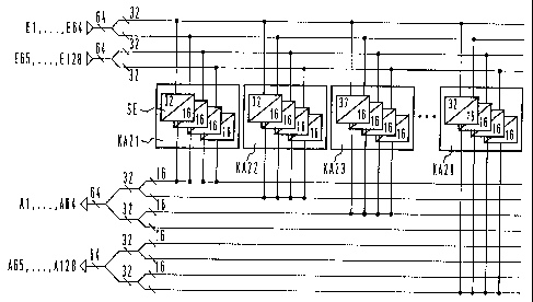
L'invention concerne une interface servant à connecter de manière sélective des lignes d'entrée (E1,..., E128) regroupées en une pluralité de groupes de lignes d'entrée, à au moins un groupe de lignes de sortie (A1,..., A16). Chacun des groupes de lignes d'entrée est connecté à un élément d'interface (SE) séparé d'au moins un agencement d'éléments d'interface (par ex. KA21) à structure conique. Chaque agencement d'éléments d'interface dispose d'un nombre de sorties correspondant au nombre de lignes de sortie appartenant à chaque groupe de lignes de sortie. Chacune de ces sorties est connectée à une des lignes de sortie appartenant au groupe de lignes de sortie correspondant. Il est prévu que chaque agencement d'éléments d'interface (KA21) ne comprenne que les éléments d'interface (SE) connectés aux groupes de lignes d'entrée. Les éléments d'interface disposent chacun de sorties associées individuellement aux lignes de sortie appartenant au groupe de lignes de sortie correspondant. Seule une des sorties de ces éléments d'interface, qui correspondent les unes aux autres, peut être connectée de manière sélective par des éléments de commutation à la ligne de sortie appropriée du groupe de lignes de sortie correspondant.


Abrégé anglais


The switching network serves for the freely
selectable connecting of input lines (E1,...,E128)
combined into a plurality of input-line groups to at
least one output-line group (A1,...,A16), on the one hand
each of the input-line groups being connected to a
separate switching element (SE) of at least one arrangement
of switching elements (for example KA21) having a
funnel structure. On the other hand, the respective
arrangement of switching elements has a number of outputs
corresponding to the number of output lines belonging to
the respective output-line group. Each of these outputs
is in connection with one of the output lines belonging
to the respective output-line group. In this case, it is
provided that the respective arrangement of switching
elements (KA21) is formed only by the switching elements
(SE) connected to the input-line groups. The switching
elements in each case have outputs which are individually
assigned to the output lines belonging to the respective
output-line group. In this case, only one of the mutually
corresponding outputs of these switching elements can be
connected, according to choice, to the relevant output
line of the respect output-line group by switching means.

Revendications

Note : Les revendications sont présentées dans la langue officielle dans laquelle elles ont été soumises.


-8-
CLAIMS:
1. Switching network for communication devices for
the freely selectable connecting of input lines (E1,...,E128)
combined into a plurality of input-line groups to at least
one output-line group (A1,...,A16), on the one hand each of
the input-line groups being connected to a separate
switching element (SE) of at least one arrangement of
switching elements (for example KA21) having a funnel
structure and on the other hand the respective arrangement
of switching elements having a number of outputs
corresponding to the number of output lines belonging to the
respective output-line group and each of these outputs being
in connection with one of the output lines belonging to the
respective output-line group, characterized in that the
respective arrangement of switching elements (KA21) is
formed only by the switching elements (SE) connected to the
input-line groups, and in that each of the switching
elements has outputs which are individually assigned to the
output lines belonging to the respective output-line group,
and in that only one of the mutually corresponding outputs
of these switching elements can be selectively connected to
the relevant output-line of the respective output-line group
by switching means.
2. Switching network according to Claim 1,
characterized in that the switching means are of such a form
that the mutually corresponding outputs of the switching
elements are connected to each other by the said switching
means in the manner of a "wired-or" operation and each of
these outputs can be controlled, to assume an active or
high-impedance state.
3. Switching network according to Claim 1,
characterized in that tree switching means are in the form of

-9-
a multiplexing device (MUX) to which on the input side the
mutually corresponding outputs of the switching elements are
led and by which one of these outputs can be selectively
connected to the relevant output-line.
4. Switching network according to one of Claims 1 to
3, characterized in that the switching means are further of
such a form that differences in signal delay at the mutually
corresponding outputs of the switching elements are
compensated by the said switching means.
5. Switching network according to one of Claims 1 to
4, characterized in that a plurality of output-line groups
are provided, in that each of the output-line groups is
assigned a separate arrangement of switching elements and in
that the input-line groups are led in parallel to mutually
corresponding switching elements of the arrangement of
switching elements relevant for the said groups.

Description

Note : Les descriptions sont présentées dans la langue officielle dans laquelle elles ont été soumises.


CA 02233467 2001-11-08
20365-3823
-1-
Description
Switching network for communication devices
The invention .relates to a switching network for
communication devices fo_r the freely selectable connecting
of input lines combined.:into a plurality of input-line
groups to at least one output-line group according to the
precharacterizing clause of Patent Claim 1. Such a
switching network is already known from "IEEE JOURNAL ON
SELECTED AREAS IN COMMUNICATIONS", Vol. 9, No. 8, October
1991, pages 1299 to 1307. In the case of this switching
network, the respective arrangement of switching elements is
in a multi-stage form of funnel structure, in order to
connect an even number of input lines in a freely selectable
way to a number of output lines corresponding to half the
number of input lines. Consequently, due to the number of
individual switching elements for realizing the funnel
structure of the respective arrangement of switching
elements, relatively corrtplex circuitry is required, which is
sometimes undesired.
It is thus the' object of the present invention to
show a way in which a switching network according to the
precharacterizing clause of Patent Claim 1 can be formed to
make it possible to reduce the complexity of the circuitry
for realizing the respective arrangement of switching
elements.
In accordance with the present invention, there is
provided a switching nei~work for communication devices .for
the freely selectable connecting of input lines (E1,...,E128)
combined into a plurality of input-line groups to at least
one output-line group (A1,...,A16), on the one hand each of
the input-line groups being connected to a separate

CA 02233467 2001-11-08
20365-3823
-1a-
switching element (SE) o:E at least one arrangement of
switching elements (for s_°xample KA21) having a funnel
structure and on the other hand the respective arrangement
of switching elements having a number of outputs
corresponding to the num'oer of output lines belonging to the
respective output-line group and each of these outputs being
in connection with one of the output lines belonging to the
respective output-line group, characterized in that the
respective arrangement of switching elements (KA21) is
formed only by the switching elements (SE) connected to the
input-line groups, and i.n that each of the switching
elements has outputs which are individually assigned to the
output lines belonging to the respective output-line group,
and in that only one of the mutually corresponding outputs
of these switching elements can be selectively connected to
the relevant output-line of the respective output-line group
by switching means.
The invention thereby brings with it, for example,
the following advantages over the prior art:
- lower number of switching elements and
consequently a cost reduction for the respective arrangement
of switching elements,
- lower power loss because of the reduction in the
number of switching elements,

CA 02233467 1998-03-27
o ,
T T
95 P 2020 - 2 -
- saving in subassembly surface area for realizing the
switching network
- and lower signal delay time because of the reduced
number of switching elements to be passed through
within the respective arrangement of switching
elements.
Advantageous refinements of the switching network
according to the present invention emerge from Patent
Claims 2 to 5.
The present invention is described in more detail
below on the basis of exemplary embodiments represented
in the drawings, in which:
FIG 1 shows a switching network according to the prior
art cited above,
FIG 2 shows in schematic form a switching network in
which the present invention is used,
FIG 3 shows a first exemplary embodiment of the
arrangements of switching elements represented in
FIG 2,
FIG 4 shows a second exemplary embodiment of the
arrangements of switching elements represented in
FIG 2, and
FIG 5 shows an exemplary embodiment of arrangements of
switching elements according to FIG 2 distributed
between two subassemblies.
In FIG l, a switching network corresponding to
the prior art cited above is represented for the case in
which 128 input lines can be connected freely selectably
to 128 output lines. The input lines are denoted by El to
E128, the output lines on the other hand are denoted by
Al to A128. The input lines and output lines are in this
case subdivided into input-line groups and output-line
groups with in each case a fixed number of input lines
and output lines, respectively. An input-line group a.s
formed here by 32 input lines, an output-line group on
the other hand is formed by 16 output lines.
Altogether, in the assumed example, four input-
line groups and 8 output-line groups are formed. Each of
the 8 output-line groups is in this case assigned a

CA 02233467 1998-03-27
95 P 2020 - 3 -
separate arrangement of switching elements. The arrange-
ments of switching elements, which are denoted by KA11 to
KA18, are connected on the input side in parallel to the
four input-line groups.
The arrangements of switching elements, having
the same structure in each case, are respectively of a
multi-stage funnel form, using switching elements with 32
inputs and 16 outputs. The switching elements are denoted
by SE. A first stage has four switching elements, which
are in each case connected to one of the input-line
groups. This is adjoined by a second stage, which is
composed of two switching elements. To their inputs there
are led the outputs of the switching elements of the
first stage. On the output side, the switching elements
of the second stage are finally in connection with a
switching element forming a third stage. This switching
element is connected by its 16 outputs to one of the
output-line groups.
The switching network represented in FIG 1 and
realized in accordance with the prior art thus has in the
assumed example 7 switching elements per arrangement of
switching elements, ie. a total of 56 switching elements.
In FIG 2 there is represented a switching network
according to the present invention which can be used, for
example, in communication devices operating on the basis
of an asynchronous transfer mode (ATM), such as for
example ATM switching devices or ATM "cross connects", in
order to be able to relay information cells fixed for
this transfer mode. Apart from the realization of the
individual arrangements of switching elements, this
switching network corresponds to the switching network
reproduced in FIG 1. The arrangements of switching
elements are denoted in FIG 2 by KA21 to KA28. These
arrangements of switching elements are in each case of
only a single-stage form, four switching elements SE with
in each case 32 inputs and 16 outputs being provided in
this single stage. Here too, to each of these switching
elements there is connected one of the input-line groups.
The outputs of the switching elements are individually

CA 02233467 1998-03-27
95 P 2020 - 4 -
assigned to the 16 outputs of an output-line group.
However, in this case only one of the mutually correspon-
ding four outputs of the switching elements which are
assigned to one and the same output line can be con-
s netted, according to choice, to the relevant output line
by switching means.
In the case of the switching network represented
in FIG 2, there are thus required in the assumed example,
in contrast to the switching network reproduced in FIG 1,
now only four switching elements per arrangement of
switching elements and consequently a total of 32 switch-
ing elements.
In FIG 3 there is indicated a first exemplary
embodiment of how the individual arrangements of switch
ing elements represented in FIG 2 are realized. In the
case of this exemplary embodiment it is assumed that 64
input lines can be connected freely selectably to 16
output lines. For this purpose, two switching elements SE
with in each case 32 input lines and 16 output lines are
provided. In this case, the previously mentioned switch-
ing means are of such a form that the mutually corre-
sponding two outputs of the switching elements which are
assigned to one and the same output line are connected to
each other by the said switching means a.n the manner of
a "wired-or" operation. Each of these two outputs can be
controlled, according to choice, to assume an active or
high-impedence state, with the result that at a given
point is time only one of the two outputs is ever con-
nected to the relevant output line. Controlling takes
place in this case via a control bus CB connected to the
two switching elements. Via this control bus the outputs
of the switching elements are also controlled in such a
way that they operate bit-synchronously. The switching
over of the outputs of the switching elements connected
to each other by the switching means may in this case
take place, for example, after the transmission of an
information cell or when a so-called void cell occurs, if
void cells are inserted at periodically recurring inter-
vals in the cell stream to be relayed to the respective

CA 02233467 1998-03-27
95 P 2020 - 5 -
output line. Irrespective of the specific type of switch-
ing over, its sequence, and consequently the sequence for
the emiss3.on of an information cell by the respective
switching element, can be fixed by the respective switch-
ing element with the aid of control signals transmitted
via the control bus CB. For example, these control
signals may be sent commands which are cyclically emitted
to the switching elements.
In FIG 4 there is indicated a further exemplary
embodiment of how the individual arrangements of switch
ing elements represented in FIG 2 are realized. This
corresponds substantially to the exemplary embodiment
described before with reference to FIG 3. There is a
difference only in the design of the switching means for
switching the mutually corresponding outputs of the
switching elements SE to a relevant output line. While in
the case of the first exemplary embodiment a "wired-or"
operation is performed, here it is provided that the
switching elements are respectively followed by a multi-
plexa.ng device MUX. The two multiplexing devices MUX have
in the assumed example eight separate pairs of inputs,
which are each individually assigned an output connected
to one of the output lines. The multiplexing devices thus
have in each case an 8X2:1 structure. Connected to a pair
of inputs are in this case the two mutually corresponding
outputs of the switching elements SE assigned to one and
the same output line, the multiplexing devices being
controllable via the control bus CB a.n such a way that,
of a pair of inputs, at every point in time there a.s only
ever one input connected to the associated output line.
The sequence of the switching over may in this case take
place as in the case of the first exemplary embodiment by
control signals transmitted via the control bus. The
exemplary embodiment represented in FIG 4 may, moreover,
in the assumed example also be modified in such a way
that, instead of multiplexing devices individually
assigned to the switching elements, only one such multi-
plexing device a.s used, which in the example has 16 pairs
of inputs, to which in each case there is individually

CA 02233467 1998-03-27
95 P 2020 - 6 -
assigned an output. This multiplexing device thus has a
16X2:1 structure.
Finally, represented in FIG 5 is the case in
which, with an arrangement of switching elements, 128
input lines can be connected freely selectably to 16
output lines. Of the four switching elements SE required
for this purpose, in this case let two be accommodated on
a subassembly A, the remaining two switching element's on
the other hand be accommodated on a subassembly B. The
outputs of the two switching elements present on one
subassembly are in this case provided with switching
means according to one of the exemplary embodiments
explained above. Since differences in the delay during
the transmission of information cells may occur because
of this separate accommodation of the switching elements
and consequently because of different line lengths, the
outputs of the two subassemblies (16 per subassembly) are
connected to a phase-matching device PH, which is con-
nected on the output side to the 16 output lines. The
said differences in delay are compensated in this case by
this phase-matching device. In the event that the switch
ing means are in the form of multiplexing devices,
according to the second exemplary embodiment, the phase
matching may also be carried out by these multiplexing
devices.
Finally, a.t should also be pointed out that the
arrangements of switching elements explained above with
reference to Figures 2 to 5 only represent expedient
designs. For example, the switching elements respectively
included in the arrangements of switching elements may
also be modifed with regard to the number of inputs and
outputs. Moreover, the internal structure of the individ-
ual switching elements may, for example, be based on a
structure such as that specified in the document cited at
the beginning. In this case, all that is necessary is to
connect to the outputs of the respective switching
element switching means corresponding to one of the
exemplary embodiments explained above.
In addition, it should also be further pointed

CA 02233467 1998-03-27
95 P 2020 - 7 -
out that the switching network explained above can be
used not only in ATM communication devices but also
generally in communication devices which are designed for
a transmission principle other than the asynchronous
transfer mode mentioned.

Dessin représentatif
Une figure unique qui représente un dessin illustrant l'invention.
États administratifs

2024-08-01 : Dans le cadre de la transition vers les Brevets de nouvelle génération (BNG), la base de données sur les brevets canadiens (BDBC) contient désormais un Historique d'événement plus détaillé, qui reproduit le Journal des événements de notre nouvelle solution interne.

Veuillez noter que les événements débutant par « Inactive : » se réfèrent à des événements qui ne sont plus utilisés dans notre nouvelle solution interne.

Pour une meilleure compréhension de l'état de la demande ou brevet qui figure sur cette page, la rubrique Mise en garde , et les descriptions de Brevet , Historique d'événement , Taxes périodiques et Historique des paiements devraient être consultées.

Historique d'événement

Description Date
Inactive : CIB expirée 2013-01-01
Le délai pour l'annulation est expiré 2008-09-17
Lettre envoyée 2007-09-17
Inactive : CIB de MCD 2006-03-12
Accordé par délivrance 2004-06-22
Inactive : Page couverture publiée 2004-06-21
Préoctroi 2004-04-01
Inactive : Taxe finale reçue 2004-04-01
Un avis d'acceptation est envoyé 2003-10-08
Lettre envoyée 2003-10-08
Un avis d'acceptation est envoyé 2003-10-08
Inactive : Approuvée aux fins d'acceptation (AFA) 2003-09-16
Lettre envoyée 2002-01-04
Modification reçue - modification volontaire 2001-11-08
Requête en rétablissement reçue 2001-11-08
Exigences de rétablissement - réputé conforme pour tous les motifs d'abandon 2001-11-08
Inactive : Abandon. - Aucune rép dem par.30(2) Règles 2001-10-12
Inactive : Dem. de l'examinateur par.30(2) Règles 2001-04-12
Retirer de l'acceptation 2001-04-11
Inactive : Approuvée aux fins d'acceptation (AFA) 2001-03-30
Inactive : CIB attribuée 1998-07-03
Symbole de classement modifié 1998-07-03
Inactive : CIB en 1re position 1998-07-03
Inactive : Acc. récept. de l'entrée phase nat. - RE 1998-06-11
Demande reçue - PCT 1998-06-09
Toutes les exigences pour l'examen - jugée conforme 1998-03-27
Exigences pour une requête d'examen - jugée conforme 1998-03-27
Demande publiée (accessible au public) 1997-04-03

Historique d'abandonnement

Date d'abandonnement Raison Date de rétablissement
2001-11-08

Taxes périodiques

Le dernier paiement a été reçu le 2003-08-14

Avis : Si le paiement en totalité n'a pas été reçu au plus tard à la date indiquée, une taxe supplémentaire peut être imposée, soit une des taxes suivantes :

  • taxe de rétablissement ;
  • taxe pour paiement en souffrance ; ou
  • taxe additionnelle pour le renversement d'une péremption réputée.

Les taxes sur les brevets sont ajustées au 1er janvier de chaque année. Les montants ci-dessus sont les montants actuels s'ils sont reçus au plus tard le 31 décembre de l'année en cours.
Veuillez vous référer à la page web des taxes sur les brevets de l'OPIC pour voir tous les montants actuels des taxes.

Historique des taxes

Type de taxes Anniversaire Échéance Date payée
Taxe nationale de base - générale 1998-03-27
Requête d'examen - générale 1998-03-27
Enregistrement d'un document 1998-03-27
TM (demande, 2e anniv.) - générale 02 1998-09-17 1998-08-17
TM (demande, 3e anniv.) - générale 03 1999-09-17 1999-08-12
TM (demande, 4e anniv.) - générale 04 2000-09-18 2000-08-18
TM (demande, 5e anniv.) - générale 05 2001-09-17 2001-08-16
Rétablissement 2001-11-08
TM (demande, 6e anniv.) - générale 06 2002-09-17 2002-08-16
TM (demande, 7e anniv.) - générale 07 2003-09-17 2003-08-14
Taxe finale - générale 2004-04-01
TM (brevet, 8e anniv.) - générale 2004-09-17 2004-08-12
TM (brevet, 9e anniv.) - générale 2005-09-19 2005-08-11
TM (brevet, 10e anniv.) - générale 2006-09-18 2006-08-14
Titulaires au dossier

Les titulaires actuels et antérieures au dossier sont affichés en ordre alphabétique.

Titulaires actuels au dossier
SIEMENS AKTIENGESELLSCHAFT
Titulaires antérieures au dossier
ATHANASE MARIGGIS
Les propriétaires antérieurs qui ne figurent pas dans la liste des « Propriétaires au dossier » apparaîtront dans d'autres documents au dossier.
Documents

Pour visionner les fichiers sélectionnés, entrer le code reCAPTCHA :


Pour visualiser une image, cliquer sur un lien dans la colonne description du document (Temporairement non-disponible). Pour télécharger l'image (les images), cliquer l'une ou plusieurs cases à cocher dans la première colonne et ensuite cliquer sur le bouton "Télécharger sélection en format PDF (archive Zip)" ou le bouton "Télécharger sélection (en un fichier PDF fusionné)".

Liste des documents de brevet publiés et non publiés sur la BDBC .

Si vous avez des difficultés à accéder au contenu, veuillez communiquer avec le Centre de services à la clientèle au 1-866-997-1936, ou envoyer un courriel au Centre de service à la clientèle de l'OPIC.

({010=Tous les documents, 020=Au moment du dépôt, 030=Au moment de la mise à la disponibilité du public, 040=À la délivrance, 050=Examen, 060=Correspondance reçue, 070=Divers, 080=Correspondance envoyée, 090=Paiement})


Description du
Document 
Date
(aaaa-mm-jj) 
Nombre de pages   Taille de l'image (Ko) 
Dessin représentatif 1998-07-07 1 11
Description 2001-11-07 8 343
Revendications 2001-11-07 2 71
Abrégé 1998-03-26 1 33
Description 1998-03-26 7 310
Revendications 1998-03-26 2 71
Dessins 1998-03-26 4 112
Abrégé 2004-04-01 1 33
Dessin représentatif 2004-05-17 1 14
Rappel de taxe de maintien due 1998-06-09 1 111
Avis d'entree dans la phase nationale 1998-06-10 1 202
Courtoisie - Certificat d'enregistrement (document(s) connexe(s)) 1998-06-10 1 116
Avis de retablissement 2002-01-03 1 172
Courtoisie - Lettre d'abandon (R30(2)) 2001-12-23 1 172
Avis du commissaire - Demande jugée acceptable 2003-10-07 1 159
Avis concernant la taxe de maintien 2007-10-28 1 171
PCT 1998-04-07 5 155
PCT 1998-03-26 6 230
Correspondance 2004-03-31 1 31