Sélection de la langue

Search

Sommaire du brevet 2235130 

Énoncé de désistement de responsabilité concernant l'information provenant de tiers

Une partie des informations de ce site Web a été fournie par des sources externes. Le gouvernement du Canada n'assume aucune responsabilité concernant la précision, l'actualité ou la fiabilité des informations fournies par les sources externes. Les utilisateurs qui désirent employer cette information devraient consulter directement la source des informations. Le contenu fourni par les sources externes n'est pas assujetti aux exigences sur les langues officielles, la protection des renseignements personnels et l'accessibilité.

Disponibilité de l'Abrégé et des Revendications

L'apparition de différences dans le texte et l'image des Revendications et de l'Abrégé dépend du moment auquel le document est publié. Les textes des Revendications et de l'Abrégé sont affichés :

  • lorsque la demande peut être examinée par le public;
  • lorsque le brevet est émis (délivrance).
(12) Brevet: (11) CA 2235130
(54) Titre français: PROCEDE DE PRODUCTION EN SERIE D'ANTENNES IMPRIMEES
(54) Titre anglais: METHOD OF MASS PRODUCING PRINTED CIRCUIT ANTENNAS
Statut: Périmé et au-delà du délai pour l’annulation
Données bibliographiques
(51) Classification internationale des brevets (CIB):
  • H01Q 01/38 (2006.01)
  • H01Q 09/30 (2006.01)
(72) Inventeurs :
  • LAMPE, ROSS W. (Etats-Unis d'Amérique)
  • VON SHEELE, CLAES HENRI (Suède)
(73) Titulaires :
  • ERICSSON, INC.
(71) Demandeurs :
  • ERICSSON, INC. (Etats-Unis d'Amérique)
(74) Agent: MARKS & CLERK
(74) Co-agent:
(45) Délivré: 2003-12-30
(86) Date de dépôt PCT: 1996-10-16
(87) Mise à la disponibilité du public: 1997-04-24
Requête d'examen: 2001-09-24
Licence disponible: S.O.
Cédé au domaine public: S.O.
(25) Langue des documents déposés: Anglais

Traité de coopération en matière de brevets (PCT): Oui
(86) Numéro de la demande PCT: PCT/US1996/016515
(87) Numéro de publication internationale PCT: US1996016515
(85) Entrée nationale: 1998-04-16

(30) Données de priorité de la demande:
Numéro de la demande Pays / territoire Date
08/544,631 (Etats-Unis d'Amérique) 1995-10-18

Abrégés

Abrégé français

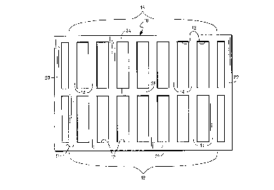
La présente invention concerne un procédé de production en série d'antennes imprimées. Ce procédé comprend la fourniture d'un substrat de matière diélectrique ayant une première et une deuxième faces, l'enlèvement de certaines parties de ce substrat pour produire un ensemble de segments interconnectés ayant les dimensions désirées, la fabrication d'un élément rayonnant principal sur la première face de chaque segment de substrat, l'enrobage de chaque segment de substrat avec une matière diélectrique protectrice et la séparation de chaque segment de substrat du substrat diélectrique pour former un certain nombre d'antennes imprimées distinctes. De préférence, il est possible d'exécuter chacune des opérations précédentes de façon sensiblement simultanée sur tous les segments de substrat. Le procédé en question peut aussi comprendre le dénudage d'une extrémité des segments de substrat, la fixation d'un connecteur électrique à chacun d'eux et l'enrobage de ce connecteur, pour chacun des segments de substrat, avant la séparation. La fabrication d'éléments rayonnants supplémentaires sur la première ou la deuxième face ou, en variante, d'un élément réactif ou parasite sur la deuxième face, peut être effectuée, de telle sorte que ces antennes imprimées soient capables de fonctionner en bandes multiples.


Abrégé anglais


A method of mass producing printed circuit antennas is disclosed including the
steps of providing a substrate of dielectric material having a first side and
a second side, removing portions of the substrate to produce an array of
interconnected segments of desired size, fabricating a main radiating element
on the first side of each substrate segment, overmolding each substrate
segment with a protective dielectric material, and separating each substrate
segment from the dielectric substrate to form a plurality of individual
printed circuit antennas. Preferably, each of the foregoing steps are able to
be performed on each substrate segment substantially simultaneously. The
method may also include the steps of freeing one end of the substrate
segments, attaching an electrical connector to each substrate segment, and
overmolding the electrical connector for each of the substrate segments prior
to the separating step. Fabrication of additional radiating elements to the
first or second side, or alternatively a reactive or parasitic element to the
second side, may be undertaken so that the printed circuit antennas are
capable of multi-band operation.

Revendications

Note : Les revendications sont présentées dans la langue officielle dans laquelle elles ont été soumises.


-10-
1. A method of mass producing printed circuit
antennas, comprising the following steps:
(a) providing a substrate of dielectric
material having a first side and a second
side;
(b) removing portions of said substrate to
produce an array of interconnected
segments having a desired size;
(c) fabricating a main radiating element on
said first side of each substrate segment;
(d) overmolding each substrate segment with a
protective dielectric material; and
(e) separating each substrate segment from
said dielectric substrate to form a
plurality of individual printed circuit
antennas.
2. The method of claim 1, wherein the fabrication
of said main radiating element on each substrate segment
occurs substantially simultaneously.
3. The method of claim 1, wherein the removal of
substrate portions to produce said array of
interconnected segments occurs substantially
simultaneously.
4. The method of claim 1, wherein said substrate
removing step and said fabricating step occur
substantially simultaneously.
5. The method of claim 1, wherein the overmolding
of each substrate segment occurs substantially
simultaneously.

-11-
6. The method of claim 1, wherein the separation
of each substrate segment from said dielectric substrate
occurs substantially simultaneously.
7. The method of claim 1, wherein said substrate
is made of a dielectric material having a minimum degree
of flexibility.
8. The method of claim 1, further comprising the
steps of freeing one end of each substrate segment and
attaching an electrical connector to the free end of each
said substrate segment prior to said separating step.
9. The method of claim 8, further comprising the
step of overmolding said electrical connector for each
said substrate segment prior to said separating step.
10. The method of claim 9, wherein the overmolding
of said electrical connector for each substrate segment
occurs substantially simultaneously.
11. The method of claim 1, wherein said overmolding
step is accomplished by injection molding.
12. The method of claim 1, further comprising the
step of removing surplus substrate material prior to
overmolding said substrate segments, wherein said
substrate segments are the approximate size of said main
radiating elements.
13. The method of claim 1, wherein said array
comprises at least one row of a plurality of
interconnected substrate segments.

-12-
14. The method of claim 1, wherein said main
radiating element is a printed trace of conductive
material.
15. The method of claim 1, wherein said main
radiating element is a monopole.
16. The method of claim 1, wherein said main
radiating element is a dipole.
17. The method of claim 1, wherein said fabricating
step occurs prior to said substrate removing step.
18. The method of claim 17, wherein each of said
substrate segments includes one of said main radiating
elements thereon.
19. The method of claim 1, further comprising the
step of fabricating at least one additional radiating
element on said first side of each substrate segment.
20. The method of claim 19, wherein the fabrication
of said additional radiating element on each substrate
segment occurs substantially simultaneously.
21. The method of claim 19, wherein the fabrication
of said main radiating element and said additional
radiating element on each substrate segment occurs
substantially simultaneously.
22. The method of claim 1, further comprising the
step of fabricating a reactive element on said second
side of each said substrate segment.

-13-
23. The method of claim 22, wherein the fabrication
of said reactive element on each substrate segment occurs
substantially simultaneously.
24. The method of claim 1, further comprising the
step of forming a parasitic element on said second side
of each said substrate segment.
25. The method of claim 24, wherein the forming of
said parasitic element on each substrate segment occurs
substantially simultaneously.
26. The method of claim 1, further comprising the
step of fabricating a second radiating element on said
second side of each said substrate segment.
27. The method of claim 26, wherein the fabrication
of said second radiating element on each substrate
segment occurs substantially simultaneously.
28. A method of mass producing printed circuit
antennas, comprising the following steps:
(a) providing a substrate of dielectric
material having a first side and a second
side;
(b) simultaneously fabricating a plurality of
main radiating elements having a specified
size on said first side of said dielectric
substrate in a predetermined pattern;
(c) simultaneously removing portions of said
dielectric substrate to produce an array
of interconnected segments of desired
size, each of said substrate segments
including one of said main radiating
elements;
(d) simultaneously overmolding each substrate

-14-
segment with a protective dielectric
material; and
(e) simultaneously separating each said
substrate segment from said dielectric
substrate to form a plurality of
individual printed circuit antennas.
29. The method of claim 28, wherein said substrate
is made of a dielectric material having a minimum degree
of flexibility.
30. The method of claim 28, further comprising the
steps of freeing one end of each substrate segment and
attaching an electrical connector to the free end of each
said substrate segment prior to said separating step.
31. The method of claim 30, further comprising the
step of overmolding said electrical connector for each
said substrate segment prior to said separating step.
32. The method of claim 28, further comprising the
step of simultaneously fabricating at least one
additional radiating element on said first side of each
substrate segment.
33. The method of claim 28, further comprising the
step of simultaneously fabricating a reactive element on
said second side of each said substrate segment.
34. The method of claim 28, further comprising the
step of simultaneously forming a parasitic element on
said second side of each said substrate segment.
35. The method of claim 28, further comprising the
step of simultaneously fabricating a second radiating
element on said second side of each substrate segment.

Description

Note : Les descriptions sont présentées dans la langue officielle dans laquelle elles ont été soumises.


CA 02235130 2002-11-15
WO 97/15093 PGT/US96/16515
-1-
METHOD OF MASS PRODUCING PRINTED CIRCUIT ANTENNAS
BACKGROUND OF TFiE LION
1. Field of the Invention
The present invention relates to printed
circuit antennas for radiating and receiving
electromagnetic signals and, more particularly, to a
method of mass producing such printed circuit antennas.
2. Descriptio~r~ of Related Art
It has been found that a monopole antenna
mounted perpendicularly to a conducting surface provides
an antenna having good radiation characteristics,
desirable drive point impedance, and relatively simple
construction. As a consequence, monopole.antennas have
been utilized with portable radios, cellular telephones,
and other personal communication systems. Until
recently, however, such monopole antennas have been
limited to wire designs (e. g., the helical configuration
in U.S. patent 5,231,412 to Eberhardt et al.), which
operate at a single frequency within an associated
bandwidth.
In order to minimize size requirements and
permit multi-band operation, while overcoming the
.disadvantages associated with microstrip and lamina
antennas, the assignee of the present invention has
recently filed several patent applications for printed
circuit antennas. It is highly desirable that such
printed circuit antennas be mass produced or
manufactured in such a way that costs are reduced and
efficiency is increased. It is also desirable that the

CA 02235130 1998-04-16
WO 97/15093 PCT/US96/16515
-2-
method of mass producing the printed circuit antennas
maintain a high level of uniformity and quality.
In light of the foregoing, a primary object of '
the present invention is to provide a process for mass
producing printed circuit antennas.
Another object of the present invention is to
provide a process for mass producing printed circuit
antennas which minimizes the time required to produce
such printed circuit antennas.
A further object of the present invention is to
provide a process for mass producing printed circuit
antennas which enables one step thereof to be performed
for all such printed circuit antennas substantially
simultaneously.
Yet another object of the present invention is
to provide a process for mass producing printed circuit
_antennas which enables more than one step thereof to be
performed for all such printed circuit antennas
substantially simultaneously.
Still another object of the present invention
is to provide a process for mass producing printed
circuit antennas which are able to operate within more
than one frequency bandwidth.
These objects and other features of the present
invention will become more readily appare~t upon
reference to the following description when taken in
conjunction with the following drawing.
~UNtMARY OF THE INVENTION
In accordance with the present invention, a
method of mass producing printed circuit antennas is
disclosed including the steps of providing a substrate of
dielectric material having a first side and a second
side, removing portions of the substrate to produce an '
array of interconnected segments of desired size,
fabricating a main radiating element on the first side of
SUBSTITUTE SHEET (RULE 26)

CA 02235130 1998-04-16
WO 97/15093 PCT/US96/165I5
-3- -
each substrate segment, overmolding each substrate
segment with a protective dielectric material, and
separating each substrate segment from the dielectric
substrate to form a plurality of individual printed
' S circuit antennas. Preferably, each of the foregoing
steps are able to be performed on each substrate segment
substantially simultaneously.
In a second aspect of the present invention,
the steps of freeing one end of the substrate segments,
l0 attaching an electrical connector to each substrate
segment, and overmolding the electrical connectors prior
to the separating step is included.
In a third aspect of the present invention, the
fabrication of additional elements to the substrate
15 segment takes place to permit multi-band operation by the
printed circuit antenna. This includes the addition of
_at least one other radiating element on either the first
or second side thereof, or alternatively a reactive
element or parasitic element fabricated on the second
20 side of each substrate segment, prior to the overmolding
step.
In a fourth aspect of the present invention,
the order of the steps for the method of the present
invention are modified so that fabrication of a plurality
25 of the main radiating elements on the first side of the
dielectric substrate is performed first and then portions
of the substrate are removed to produce an array of
interconnected substrate segments which each include one
of the main radiating elements.
30 BRIEF DESCRIPTION OF THE DRAWING
While the specification concludes with claims
particularly pointing out and distinctly claiming the
' present invention, it is believed that the same will be
better understood from the following description taken in
35 conjunction with the accompanying drawing in which:
SUBSTITUTE SHEET (RULE 26)

CA 02235130 1998-04-16
WO 97/15093 PCT/L1S96/16515
-4- -
Fig. 1A is a schematic top view of a dielectric
substrate with portions of the substrate removed to
depict a plurality of interconnected substrate segments; .
Fig. 1B is a schematic top view of a dielectric
substrate with a plurality of radiating elements
fabricated thereon in a predetermined pattern;
Fig. 2 is a schematic top view of the
dielectric substrate of Fig. 1A in which a main radiating
element has been fabricated on each substrate segment or
a schematic top view of the dielectric substrate depicted
in Fig. 1B in which portions of the substrate have been
removed to form a plurality of interconnected substrate
segments which each include a main radiating element
previously formed on the dielectric substrate,
respectively;
Fig. 3 is a schematic top view of the
dielectric substrate of Fig. 2 with the top side of the
substrate segments being overmolded;
Fig. 4 is a schematic top view of the
dielectric substrate depicted in Fig. 3 in which an
electrical connector has been attached to each substrate
segment;
Fig. 5 is a schematic top view of the
dielectric substrate of Fig. 4 in which the electrical
connectors have been overmolded;
Fig. 6 is a schematic top side view of an
individual printed circuit antenna after being separated
from the dielectric substrate depicted in Fig. 5;
Fig. 7 is a schematic top side view of the
dielectric substrate depicted in Fig. 2, wherein an
additional radiating element has been fabricated on each
substrate segment; '
Fig. 8 is a schematic bottom side view of the
dielectric substrate depicted in Fig. 2, wherein a
reactive element has been fabricated on each substrate
segment;
SUBSTITUTE SHEET (RULE 26)

CA 02235130 1998-04-16
WO 97/15093 PCT/US96/16515
-5- -
Fig. 9 is a schematic bottom side view of the
dielectric substrate depicted in Fig. 2, wherein a
' parasitic element has been formed on each substrate
segment; and
Fig. 10 is a schematic bottom side view of the
dielectric substrate depicted in Fig. 2, wherein a second
radiating element has been fabricated on each substrate
segment.
DETAILED DESCRIPTION OF T~iE INVENTION
Referring now to the drawings in detail,
wherein identical numerals indicate the same elements
throughout the figures, Fig. 1A depicts a dielectric
substrate identified generally by the numeral 10 in which
portions of substrate 10 have been removed to form a
plurality of open areas or cutouts 12 and a plurality of
_ interconnected substrate segments 14. As will be seen
therein, substrate segments 14 are arrayed in a pair of
adjacent rows 16 and 18, although the arrangement of such
substrate segments 14 may be in any desirable manner. In
order for substrate segments 14 to remain interconnected
throughout the process of the present invention, a pair
of side portions 20 and 22 of dielectric substrate 10
remain, as does a top portion 24, a middle portion 26,
and a bottom portion 28.
Instead of first forming the individual
substrate segments 14 as shown in Fig. 1A, the method of
mass producing printed circuit antennas may alternatively
involve fabricating a plurality of main radiating
elements 30 in a conductive material of desired size on
dielectric substrate l0 in a predetermined pattern prior
' to forming individual substrate segments 14 as shown in
Fig. 1B.
' In either event, as seen in Fig. 2, substrate
segments 14 each have a main radiating element 30
fabricated on a top side 32 thereof. This is
SUBSTITUTE SHEET (RULE 26)

CA 02235130 1998-04-16
WO 97/15093 PCT/US96/16515
-6-
accomplished by fabricating main radiating elements 30
onto substrate segments 14 when beginning with the
dielectric substrate shown in Fig. 1A or removing
portions of dielectric substrate 10 to form substrate
segments 14 which include a main radiating element 30
when beginning with the dielectric substrate depicted in
Fig. 1B. While it is preferred that each substrate
segment 14 be initially sized to closely approximate the
size of main radiating element 30, an optional trimming
step for each substrate segment 14 may take place if
necessary.
Thereafter, as depicted in Fig. 3, it is
preferred that each substrate segment 14 be overmolded
with a protective dielectric material (indicated by the
numeral 33), preferably in a substantially simultaneous
fashion. This may be accomplished by placing dielectric
substrate 10 in an appropriate injection molding machine
so the overmolding is applied as desired.
Once the overmolding of substrate segments 14
has been performed, each substrate segment 14 is then
separated from dielectric substrate 10 (i.e., from top
and middle portions 24 and 26, respectively), as
applicable, to become an individual printed circuit
antenna 34 as depicted in Fig. 6.
It will be noted that it is preferred that each
of the foregoing steps in the process (i.e., forming the
plurality of substrate segments 14, fabricating main
radiating elements 30 on each substrate segment 14,
overmolding each substrate segment 14, and separating
each substrate segment 14 from dielectric substrate 10)
will preferably occur substantially simultaneously for
each substrate segment 14. In this way, the method of
the present invention saves time and thereby increases
efficiency. Likewise, it is preferred that the steps of
forming each substrate segment 14 and fabricating main
radiating elements 30 thereon, while shown as being
SUBSTITUTE SHEET (RULE 26)

CA 02235130 2003-O1-10
WO 97/15093 PCT/US96/165I5
separate steps in Figs. 1A and 1B, occur substantially
simultaneously.
Optionally, the method of the present invention
may include the steps of freeing one end of substrate
segments 14 and attaching an electrical connector 36
(e. g., a coaxial connector) to free end 38 of each
substrate segment 14 prior to separation from dielectric
substrate 10. For example, electrical connector 36 may
be attached to each substrate segment 14 by means of a
soldering or gluing process. Afterward, it would be
preferred for electrical connectors 36 to also be given
an overmolding layer 37 for each substrate segment 14,
with the overmolding of all such electrical connectors 36
occurring substantially simultaneously.
IS It will be understood from the previously
identified related patent applications that dielectric
_substrate ZO is preferably made of a dielectric material,
such as polyamide, polyester, or the like, having a
minimum degree of flexibility. This riot only meets the
requirements of the end environment for printed circuit
antennas 34, but also assists during production by
providing some degree of tolerance within the environment
of the machinery utilized.
It will further be understood that main
radiating element 30 is preferably a printed trace of
.conductive material such as copper or conductive ink.
Main radiating element 30 will normally have a non-linear
configuration in which its electrical length is greater
than its physical length to minimize its size.

i
CA 02235130 2003-02-20
T, WO 97/15093 PCT/US96/16515
_g_
At least one additional radiating element 40 may
be positioned on top side 32 of each substrate segment
14. While radiating element 40 is shown as being
linear, it may have any desired configuration.
Additional radiating element 40 preferably is
fabricated adjacent main radiating element
30 prior to overmolding of substrate segments 14. In
this way, the individual printed circuit antenna 34
1o depicted in Fig. 7 may be utilized within multiple
bandwidths. Of course, it is preferred that any
additional radiating elements 40 be fabricated on each
substrate segment 14 substantially simultaneously.
Optimally, main radiating elements 30 and additional
radiating elements 40 would be fabricated on each
substrate segment 14 substantially simultaneously.
Other alternative steps which may be taken. to
permit printed circuit antennas 34 to operate Within
multiple bandwidths include fabricating a reactive
element 42 on a bottom side 44 of each substrate segment
14 (preferably adjacent free end 38), forniing a parasitic
element 46 on bottom side 42 of each substrate segment 14
(preferably opposite free end 38 as shown in Fig. 9), or
fabricating a second radiating element 48.on bottom side
42 of each substrate segment 14 (as shown in Fig. 10).
In each case, it will be understood that it is preferred
that all reactive elements 40, parasitic elements 44, or
second radiating elements 46 be fabricated or formed
substantially simultaneously for each substrate segment
14. Of course, the addition of such elements should take
place before substrate segment 14 is overmolded.

CA 02235130 2003-O1-10
WO 97/15093 PCT/US96/16515
_g_
Having shown and described the preferred
embodiments of the present invention, further adaptations
of the method for mass producing printed circuit antennas
disclosed herein can be accomplished by appropriate
modifications by one of ordinary skill in the art without
departing from the scope of the invention. In
particular, while main radiating element 30 herein has
been shown and described as a monopole, it can easily be
a dipole by properly configuring the conductive traces
therefor. Also, as previously stated herein, the
arrangement or configuration of substrate segments 14 in
dielectric substrate 10 prior to separation may be in any
given form and need not be limited to the pair of rows
depicted herein.

Dessin représentatif
Une figure unique qui représente un dessin illustrant l'invention.
États administratifs

2024-08-01 : Dans le cadre de la transition vers les Brevets de nouvelle génération (BNG), la base de données sur les brevets canadiens (BDBC) contient désormais un Historique d'événement plus détaillé, qui reproduit le Journal des événements de notre nouvelle solution interne.

Veuillez noter que les événements débutant par « Inactive : » se réfèrent à des événements qui ne sont plus utilisés dans notre nouvelle solution interne.

Pour une meilleure compréhension de l'état de la demande ou brevet qui figure sur cette page, la rubrique Mise en garde , et les descriptions de Brevet , Historique d'événement , Taxes périodiques et Historique des paiements devraient être consultées.

Historique d'événement

Description Date
Le délai pour l'annulation est expiré 2007-10-16
Lettre envoyée 2006-10-16
Inactive : CIB de MCD 2006-03-12
Accordé par délivrance 2003-12-30
Inactive : Page couverture publiée 2003-12-29
Inactive : Taxe finale reçue 2003-10-14
Préoctroi 2003-10-14
Un avis d'acceptation est envoyé 2003-04-29
Lettre envoyée 2003-04-29
Un avis d'acceptation est envoyé 2003-04-29
Inactive : Approuvée aux fins d'acceptation (AFA) 2003-04-11
Modification reçue - modification volontaire 2003-02-20
Modification reçue - modification volontaire 2003-01-10
Modification reçue - modification volontaire 2002-11-15
Inactive : Dem. de l'examinateur par.30(2) Règles 2002-07-18
Modification reçue - modification volontaire 2002-05-08
Lettre envoyée 2001-10-15
Requête d'examen reçue 2001-09-24
Exigences pour une requête d'examen - jugée conforme 2001-09-24
Toutes les exigences pour l'examen - jugée conforme 2001-09-24
Inactive : CIB attribuée 1998-07-20
Symbole de classement modifié 1998-07-20
Inactive : CIB en 1re position 1998-07-20
Inactive : Notice - Entrée phase nat. - Pas de RE 1998-06-26
Demande reçue - PCT 1998-06-25
Demande publiée (accessible au public) 1997-04-24

Historique d'abandonnement

Il n'y a pas d'historique d'abandonnement

Taxes périodiques

Le dernier paiement a été reçu le 2003-10-03

Avis : Si le paiement en totalité n'a pas été reçu au plus tard à la date indiquée, une taxe supplémentaire peut être imposée, soit une des taxes suivantes :

  • taxe de rétablissement ;
  • taxe pour paiement en souffrance ; ou
  • taxe additionnelle pour le renversement d'une péremption réputée.

Les taxes sur les brevets sont ajustées au 1er janvier de chaque année. Les montants ci-dessus sont les montants actuels s'ils sont reçus au plus tard le 31 décembre de l'année en cours.
Veuillez vous référer à la page web des taxes sur les brevets de l'OPIC pour voir tous les montants actuels des taxes.

Historique des taxes

Type de taxes Anniversaire Échéance Date payée
Enregistrement d'un document 1998-04-16
Taxe nationale de base - générale 1998-04-16
TM (demande, 2e anniv.) - générale 02 1998-10-16 1998-10-16
TM (demande, 3e anniv.) - générale 03 1999-10-18 1999-10-06
TM (demande, 4e anniv.) - générale 04 2000-10-16 2000-10-10
Requête d'examen - générale 2001-09-24
TM (demande, 5e anniv.) - générale 05 2001-10-16 2001-10-11
TM (demande, 6e anniv.) - générale 06 2002-10-16 2002-10-08
TM (demande, 7e anniv.) - générale 07 2003-10-16 2003-10-03
Taxe finale - générale 2003-10-14
TM (brevet, 8e anniv.) - générale 2004-10-18 2004-10-04
TM (brevet, 9e anniv.) - générale 2005-10-17 2005-10-04
Titulaires au dossier

Les titulaires actuels et antérieures au dossier sont affichés en ordre alphabétique.

Titulaires actuels au dossier
ERICSSON, INC.
Titulaires antérieures au dossier
CLAES HENRI VON SHEELE
ROSS W. LAMPE
Les propriétaires antérieurs qui ne figurent pas dans la liste des « Propriétaires au dossier » apparaîtront dans d'autres documents au dossier.
Documents

Pour visionner les fichiers sélectionnés, entrer le code reCAPTCHA :


Pour visualiser une image, cliquer sur un lien dans la colonne description du document. Pour télécharger l'image (les images), cliquer l'une ou plusieurs cases à cocher dans la première colonne et ensuite cliquer sur le bouton "Télécharger sélection en format PDF (archive Zip)" ou le bouton "Télécharger sélection (en un fichier PDF fusionné)".

Liste des documents de brevet publiés et non publiés sur la BDBC .

Si vous avez des difficultés à accéder au contenu, veuillez communiquer avec le Centre de services à la clientèle au 1-866-997-1936, ou envoyer un courriel au Centre de service à la clientèle de l'OPIC.


Description du
Document 
Date
(aaaa-mm-jj) 
Nombre de pages   Taille de l'image (Ko) 
Dessin représentatif 1998-07-23 1 8
Description 2003-01-09 9 386
Description 2003-02-19 9 380
Abrégé 1998-04-15 1 73
Description 1998-04-15 9 394
Dessins 1998-04-15 10 187
Revendications 1998-04-15 5 167
Description 2002-11-14 9 394
Rappel de taxe de maintien due 1998-06-28 1 111
Avis d'entree dans la phase nationale 1998-06-25 1 193
Courtoisie - Certificat d'enregistrement (document(s) connexe(s)) 1998-06-25 1 116
Rappel - requête d'examen 2001-06-18 1 118
Accusé de réception de la requête d'examen 2001-10-14 1 179
Avis du commissaire - Demande jugée acceptable 2003-04-28 1 160
Avis concernant la taxe de maintien 2006-12-10 1 173
PCT 1998-04-15 8 233
Correspondance 2003-10-13 1 31