Note : Les descriptions sont présentées dans la langue officielle dans laquelle elles ont été soumises.
CA 02254407 1998-11-17
METHOD AND APPARATUS FOR A FLEXIBLE
ACCESS RATE COMMON-MEMORY PACKET SWITCH
TECHNICAL FIELD
The present invention relates generally to methods
and apparatus for switching data packets in a communications
network. In particular, it relates to a method of providing
flexible memory access in a dynamically configurable common
memory data packet switch which may be used for unicast
and/or multicast packet switching applications.
BACKGROUND OF THE INVENTION
The escalating demand for telecommunications
bandwidth has placed a strain on existing service delivery
infrastructure and created a desire for faster and more
efficient data delivery networks. The principal elements in
a switched data network which determine the bandwidth
capacity are the switching nodes. Many switching node
architectures have been invented for efficiently switching
data packets at high speeds. Data packet switching nodes
have been traditionally constructed with equal ingress and
egress capacities and with symmetrical ingress/egress port
configurations. A symmetrical configuration is suitable if
the capacity requirement of the connection to each port is
identical in opposite directions. In a modern multiservice
network, however, a connection may have vastly different
data rates in opposite directions. For example, the
connection from a user to a database may have a data rate of
about 1 kb/s, whereas the connection from the database to
the user may require 100 kb/s, or more. If such asymmetry
is permanent, the user may be connected to the network by
asymmetrical outbound and inbound links. If the asymmetry
is time-variant, however, the links connecting the user to
- 1 -
CA 02254407 1998-11-17
the network must be of a sufficiently high capacity to
accommodate the peak rates in both directions.
Of the many data packet switch architectures that
have been invented, one of the most widely used is the
common-memory (CM) switch. This type of switch is widely
used in data packet networks, such as ATM networks for
example. In a CM switch, the switch capacity is limited by
the CM access speed. In a non-blocking CM implementation,
the sum of the port capacities (expressed in bits per
second) is less than, or equal to, the capacity of the CM.
In such switches, the ports normally access the CM in a
sequential cycle, each port being given an equal time window
in which to write packets to, or read packets from, the CM.
This often results in idle periods when ports have no
payload packets to write to, or read from, the CM. Any idle
capacity resulting from port under-utilization cannot be
recovered if the ports access the CM for a fixed period of
time in each access cycle.
Asymmetrical unicast connections such as the one
described above place traffic loads on the ingress and
egress sides of a port which may differ significantly, but
the total ingress rate of all input ports is always equal to
the total egress rate of all output ports. In modern
multiservice networks, multicasting is frequently required.
Multicasting involves switching data from one input source
to a plurality of outputs. When multicasting occurs,
however, not only are the connection bit rates naturally
asymmetrical, but the total egress rate may substantially
exceed the total ingress rate. Therefore, switching
multicast traffic using a symmetrical switch results in
unavoidable core capacity wastage.
There therefore exists a need for an effective
method of control port access to the common-memory in CM
- 2 -
CA 02254407 1998-11-17
switches to maximize core utilization and switch throughput.
There also exists a need for a CM switch architecture for
efficiently switching unbalanced unicast traffic loads using
an asymmetrical port access capacity. There further exists
a need for a CM switch architecture which is especially
adapted for multicasting to ensure that valuable core
resources are efficiently utilized in network applications
where multicasting is consistently required.
SUMMARY OF THE INVENTION
It is an object of the invention to provide a
method of controlling asymmetrical port access in a common-
memory multi-port data packet switch.
It is a further object of the invention to provide
a method of controlling asymmetrical port access in a
common-memory multi-port data packet switch utilizing an
inexpensive, easily implemented, mechanism for generating
port access time slot identifiers to ensure that the common
memory is utilized to its full potential while packet fitter
and transit delay are reduced.
It is a further object of the invention to provide
a common-memory switch architecture which is specifically
designed to efficiently switch data packets in multicast
switching applications.
It is yet a further object of the invention to
provide a large capacity data packet switch with a folded
configuration which is particularly adapted for efficiently
multicasting data packets.
The invention therefore provides a method of
controlling port access in a common-memory multi-port data
packet switch, comprising:
defining a control cycle consisting of a fixed
number of discrete common-memory access time slots;
- 3 -
CA 02254407 1998-11-17
allocating a proportional number of the access
time slots to each port based on a predetermined access
capacity requirement for the port; and
distributing access time slots for each port in
the control cycle in such a way as to reduce packet transfer
delay and fitter.
In accordance with a further aspect of the
invention, there is provided a flexible access rate common-
memory packet switch, comprising:
a plurality of input ports and output ports;
a common-memory for switching packets between the
input ports and the output ports;
means for storing an allocation of common-memory
access time slots for each port, the allocation being based
on a predetermined access capacity requirement for the port;
and
means for distributing the access time slots for
each port in a control cycle of all access time slots
allocated in such a way that each port accesses the common-
memory in a cyclic sequence of substantially equally spaced
access time slot intervals.
The invention therefore provides a method and an
apparatus for a flexible access rate common-memory packet
switch. In accordance with the method, a common-memory-
access time period for a port of the common-memory switch is
defined. The common-memory-access time period is an
interval that is long enough to write a predetermined number
of bytes or a predetermined number of cells to the common-
memory of the switch. The common-memory-access time period
may be long enough to write a large number of bytes or cells
to, or read a large number of bytes or cells from, the
common-memory. The access time periods are hereinafter
referred to as access time slots. A common-memory-access
- 4 -
CA 02254407 1998-11-17
control table is data filled to control access by each port
to the common-memory core of the switch. The common-memory-
access control table stores an access time allocation for
each port. Each access time allocation consists of one or
more access time slots, and each access time slot is
identified by a time slot identifier. The access time
allocation is preferably proportional to the committed
access rate for each port . The access time allocation may
be performed periodically by a predictive algorithm for
predicting the traffic load for each port based on traffic
measurements. In that case, the predictive algorithm
monitors traffic loads at each port and periodically updates
the access time allocation for each port based on short term
traffic load predictions or short term traffic load
measurements. Using such a feature requires an input buffer
of adequate capacity at each node. Regardless of how the
contents of common-memory-access control table is
determined, the purpose of the table is to allocate CM
access time slots to the ports in order to maximize usage of
the core resources by the input and output ports of the
switch. With proper control, the total capacity of the
input and output ports may significantly exceed the core
capacity of the switch, without undue risk of packet loss or
service degradation.
After the time slot identifiers have been stored
in the common-memory-access control table, an upper bound
and a lower bound of the time slot identifiers for each port
are broadcast to the individual port controllers which store
the two bounds in registers reserved for that purpose.
During switch operation, each port controller receives a
time slot identifier, or receives a signal which it
transforms into a time slot identifier. Each port checks
the time slot identifier against its lower bound and its
- 5 -
CA 02254407 1998-11-17
upper bound registers to determine whether the time slot
identifier is within the port's allocated range. If the
time slot identifier is within the allocated range, the port
controller accesses the common-memory to read or write
packets or cells. The mechanism for generating time slot
identifiers preferably distributes the access time periods
so that access to the core memory by each port is as equally
spaced as possible to ensure that packet fitter is reduced.
The time slot identifiers are preferably generated
by a cyclic counter of large period (16,384 for example)
called an access control cycle. A good distribution of time
slot identifiers can be achieved by reading a binary
representation of the cyclic counter in reverse.
In accordance with a further aspect of the
invention, there is provided an architecture for a large
capacity CM switch which is expressly designed for multicast
applications. The switch architecture may include more
output ports than input ports, but it is preferably
symmetrical. A symmetrical switch is one that has an equal
number of ports which are collectively of equal capacity on
each side (ingress and egress). In a symmetrical switch in
accordance with the invention, the ports need not be of
equal capacity and in the discussion which follows it is
assumed that the ports may not be of collectively equal
capacity on each side. If a symmetrical architecture is
used, the total combined capacity of all input and output
ports preferably exceeds the core capacity. Access to the
input and output ports is controlled as described above to
maximize core usage.
Very high-capacity switches are best constructed
using a folded architecture in which a plurality of CM
switches are interlinked by middle buffers that permit the
movement of intermodular data traffic between CM modules.
- 6 -
CA 02254407 1998-11-17
With heavy multicasting, a single stand-alone configurable
CM switch can realize a multicast capacity gain of almost 2
to 1, i.e., the switch can emit almost twice as many bits
per second (b/s) into the network as a prior art packet
switch with the same CM and port configuration. For a large
scale mufti-module folded configuration switch with flexible
CM access rate allocation, a higher multicast capacity gain
can be realized. Using 64 folded CM modules, each with a
capacity of 20 Gb/s, for example, the egress capacity would
be 640 Gb/s with fixed-rate ports, whereas with flexible CM
access rate allocation, the egress capacity can exceed
2 Terabits/s at high multicast levels.
BRIEF DESCRIPTION OF THE DRAWINGS
The invention will now be further explained by way
of example only and with reference to the following
drawings, wherein:
Fig. 1 is a schematic representation of core
capacity utilization in a prior art CM packet switch;
Fig. 2 is a schematic illustration of the capacity
available for added ports in a CM packet switch when a
flexible access rate is utilized to control access to the
common-memory by the input and output ports;
Fig. 3 is a schematic illustration of the time
slots allocated in a CM packet switch having symmetrical
sides and asymmetrical CM access in a 6 X 6 packet switch;
Fig. 4 is a simplified illustration of the
distribution of CM access by the ports of a 2 X 2 CM packet
switch using a simple 4-bit counter and a reverse-binary
scatter transform to generate time slot identifiers for
controlling port access to the CM;
Fig. 5 is a schematic diagram of a CM packet
switch in accordance with the invention;
CA 02254407 1998-11-17
Fig. 6, which appears on sheet 5 of the drawings,
is a schematic diagram of CM core utilization in a
symmetrical CM packet switch during heavy multicasting;
Fig. 7, which appears on sheet 2 of the drawings,
is a schematic illustration of data flow through a CM module
of a high capacity packet switch with a folded architecture;
Fig. 8a is a schematic diagram of a prior art high
capacity switch consisting of an array of M folded
symmetrical CM modules;
Fig. 8b is a schematic diagram of the high
capacity switch configured in accordance with the invention
for use in multicasting;
Fig. 9a is a table showing the number of cells
transferred by the CM modules during an access interval (a
period of time during which each input port and each output
port has access to a particular middle buffer) in a large
capacity switch of the type illustrated in Fig. 8a; and
Fig. 9b is a table showing the number of cells
transferred by the CM modules during an access interval in a
large capacity switch of the type illustrated in Fig. 8b.
DETAINED DESCRIPTION OF THE PREFERRED EMBODIMENT
The present invention relates to a method and
apparatus for maximizing core utilization in a CM data
packet switch by allocating CM access time to the individual
ports of the data packet switch in accordance with committed
access capacity and/or predicted traffic load for each port.
A basic asynchronous transfer mode (ATM) CM switch
is constructed as a cell-wide bus connected to a cell-wide
array of memories, constituting the CM. The CM is accessed
cyclically by N dual ports (N input and N output ports).
During a CM access time period, a minimum of one cell is
written to, or read from, the CM by a port. The capacity of
_ g _
CA 02254407 1998-11-17
a CM switch is determined by the CM's access speed. For
example, an access time (read + write) of 21 nsec in an ATM
switch (i.e., one 424-bit cell per 21 nsec) yields a 20 Gb/s
switch.
Fig. 1 is a schematic illustration of core
capacity utilization by a fixed access rate prior art CM
packet switch. The core capacity 10 is represented by a
horizontal bar which is divided into eight equal sections
representative of the equal CM access time periods for the
eight ports (four input ports and four output ports) of a
4 X 4 switch. A shaded portion 12 represents the part of
each allocated access time period utilized by a port to
access the CM during its fixed CM access time interval. As
is apparent, some ports are busier than others due to
traffic load. Because of the fixed time interval which each
port has to access the CM of the packet switch, however,
core resources are under-utilized when a port experiences
little traffic.
In a symmetrical switch with N identical dual
ports, the access rate to the CM by each port is R b/s at
input and R b/s at output, and the CM dual-access (ingress
and egress) rate is C b/s at ingress and C b/s at egress,
with C >- N R. In a symmetrical switch configuration, the
total ingress rate C equals the total egress rate C. If
traffic is aggregated using multiplexers, there is higher
utilization of the core capacity. The sources should be
grouped at the ports to provide appropriate traffic
concentration. It is not always feasible to aggregate
traffic, however, and port capacity may remain under
utilized.
The number of ports of capacity R, in a
symmetrical configuration is N = ~C/R~. If the port access
rate is dynamically regulated, provided that the sum of the
- 9 -
CA 02254407 1998-11-17
ingress rates does not exceed C, a packet switch
configuration with a number of ports greater than N can be
realized. Such a packet switch configuration easily
accommodates temporal variation in the connections'
asymmetry.
Fig. 2 schematically illustrates the utilization
of the core capacity 10 shown in Fig. 1 in a switch having
an adaptive access rate in which the access rates are
allocated to efficiently use core capacity.
Without CM access control, the port capacity of a
switch is fixed at its predetermined value, 620 Mb/s for
example. In a 20 Gb/s switch, the maximum number of ports
with fixed port rate of 620 Mb/s is 32. With a flexible CM
access rate, the number of ports may be increased to 64, for
example, and the traffic loads to the ports may vary
considerably, both spatially and temporally, provided that
the total traffic load at any given moment is less than the
CM capacity.
The allocation of CM access time to the ports is
preferably updated in response to traffic load variations.
The access time slot identifiers are stored in a common
memory-access control table, as will be explained below in
further detail. The control table is inspected to determine
the CM access time allocation for each port at least as
often as the switch undergoes an initialization process,
well known in the art. In a preferred embodiment of the
invention, the common-memory-access control table is
periodically updated to ensure maximum CM utilization. The
CM access time allocations written in the common-memory-
access control table may be computed by a predictive
algorithm which collects port usage data and directly or
predictively allocates CM access time accordingly.
Alternatively, the traffic measurements or predictive
- 10 -
CA 02254407 1998-11-17
algorithm may operate at the network control level and
common-memory-access control table data may be downloaded to
a CM packet switch in accordance with the invention from a
network control centre. The frequency of update of the
common-memory-access control tables is a matter of design
choice. The update may occur every few control cycles,
every 4th control cycle, for example. The predictive
algorithms) is not a part of this invention.
The initial or default CM access time allocation
for any given CM packet switch port is set to accommodate
the maximum committed service rate for the port, which may
be less than the physical capacity of the port. Port access
to the CM must be coordinated in order to ensure that ports
do not attempt to access the CM concurrently. In order to
regulate port access to the CM, a simple solution is to
allocate contiguous bands of access time slot identifiers
proportioned in accordance with committed access capacity or
predicted traffic loads for a port. Contiguous access to
the CM by a port is not preferred, however, because packet
or cell transit delays could be unacceptably long and severe
cell fitter could result. This is avoided by using the
method in accordance with the invention to generate time
slot identifiers so that CM access time slots for each port
are distributed as evenly as possible.
In accordance with the method of generating time
slot identifiers, C represents the CM capacity in
bits/second in each direction (C ingress, C egress), R the
capacity per port in bits/second, and N the number of dual
ports (N ingress and N egress). The sum of the port
capacities may be greater than the CM capacity, i.e.,
NR >_ C. Let S be the number of access time slots per CM
access control cycle (S = 16384, for example). The service
- 11 -
CA 02254407 1998-11-17
rate per access time slot, i.e., the granularity of the data
rate, is then C/S.
Let a~ be the service rate allocation for input
port j and x~, 0 <_ j < N, be the number of assigned access
time slots per control cycle for input port j , the integer
x~ is then determined as: x~ = ray S/C~, where r.~ denotes
the next higher integer. The actual service rate allocation
for input port j is then: A~ = x~ C/S; A~ >_ a~ .
Similarly, on the egress side, if b~, 0 <_ j < N,
is the required service rate for output port j, and y~,
0 <_ j < N, is the number of assigned access time slots per
control cycle for output port j, then y~ _ (~b~ S/C~ and the
actual service rate allocation for output port j is:
B~ = y~ C / S; B~ >_ b~ .
For a non-blocking, flexible access-rate switch, we have:
N-1 N-1
E xk <_ S, and E yk _< S,
k=0 k=0
i.e., the sum of the allocated access capacities on either
the ingress or egress side is limited by the capacity C:
N-1 N-1
~ Ak <_ C, and ~ Bk 5 C,
k=0 k=0
with Ak <_ R and Bk <_ R, 0 <_ k < N.
In order to reduce cell-transfer delay, the x~
access time slots should not occupy contiguous positions in
the CM access control cycle. They can be spread almost
evenly in the control cycle as follows: Generate the
sequences
Xj . Xj ~ x~-1 + X~_1, 1 <_ j < N, with Xo = 0; and
Yj . Yj ~ y~_1 + Y~-1, 1 5 j < N, with Yo = XN.
- 12 -
CA 02254407 1998-11-17
These sequences are used to generate time slot identifiers
for controlling port access to the CM, as will be explained
below in detail (YNis the length of the control cycle).
The preferred mechanism for generating time slot
identifiers is a simple mapping method using a reverse-
binary representation of an integer count. In accordance
with the method, a cyclic counter of large period (16,384
for example) called the access control cycle is read in
reverse: i.e., the most significant bit is treated as the
least significant bit and the least significant bit is
treated as the most significant bit. The counter is
preferably incremented at an interval equal to the time
required to read/write a predefined number of packets or
cells (usually 1) to the CM. As described above, the
common-memory-access control table defines a contiguous band
of access time slot identifiers allocated to each port of
the CM packet switch. The contiguous bands are preferably
defined in the table using a lower bound integer and an
upper bound integer. If k denotes the reverse-binary number
representation of the counter, input port j accesses the CM
if
X~ <_ k < X~+1.
Similarly, output port j accesses the CM if:
Y~ <_ k < Y~+1.
The integer k is the time slot identifier corresponding to
the reading of the counter. Thus, the CM access time slot
identifiers for the ports are mutually exclusive and only
one port can access the CM during any given time slot. The
lower and upper bounds for ingress port j are X~ and X~+1-l,
and similarly the lower and upper bounds for egress port j
are Y and Y~+1-1, 0 <_ j < N.
- 13 -
CA 02254407 1998-11-17
A simple representation of this method is shown in
Fig. 4 where a 4 bit cyclic counter is used to control
access by four ports to a CM using asymmetrical CM access
time allocations. As is shown in Fig. 4, port 1 is
allocated time slots identified by numbers 0-2; port 2 is
allocated access time slots identified by numbers 3-7;
port 3 is allocated time slots identified by numbers 8-10;
and, port 4 is allocated time slots identified by
numbers 11-15. The scatter transform used to convert the
cyclic count to time slot identifiers may be any algorithm
for achieving well-spaced access times. In accordance with
the preferred embodiment of the invention, the scatter
transform is most simply and economically realized by hard
wiring a cyclic digital counter so that it may be read in
reverse. The cyclic counter is preferably of a finite word
length having a range equal to the total CM access time
slots allocated in the common-memory-access control table.
The result achieved is illustrated in Fig. 4. The time slot
identifiers generated by the scatter transform and the port
access sequence are shown on the right side of Fig. 4.
It is readily apparent that the port access
sequence is well distributed in the time domain and cell
fitter is thereby reduced. It will also be readily
appreciated by those skilled in the art that the actual
period of the cyclic counter is a function of the number of
ports and is normally much larger than that shown in Fig. 4.
The period of the cyclic counter is conveniently a power
of 2, though that is not essential. The scatter transform
could be implemented in software, but the reverse-wired
digital counter is considered the most economical
implementation and has the advantage of being very fast.
It will be understood by those skilled in the art
that the scatter transform may be implemented at the central
- 14 -
CA 02254407 1998-11-17
controller of the CM switch, in which case time slot
identifiers are broadcast to the port controllers, or at
each port controller, in which case the count is broadcast
to the port controllers and the port controllers apply the
scatter transform to produce the time slot identifiers.
As may be seen in Fig. 4, the access time slot
allocations are asymmetrically distributed among the four
ports. A primary feature of the invention is that the
allocation of access time slots may be asymmetrical between
ports and between the ingress and egress sides of the same
port. This permits a flexible, dynamic configuration of
switch resources in response to a committed access capacity
for each port or predicted or measured traffic fluctuations.
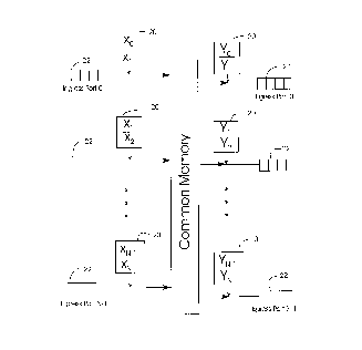
Fig. 5 shows a schematic illustration of a CM
packet switch with flexible port access rates in accordance
with the invention. The access time slots for any port are
determined by a simple comparison between the reverse-binary
of the cyclic counter and the upper and lower bound values
of the access time slot identifiers. As explained above,
the upper and lower bound values may be passed to the port
controllers from the common-memory-access control table.
The upper and lower bound values are stored in registers 20
at each port controller. For example, if a port is
allocated CM access time slots in a band of 1000-1080 in a
control cycle having a length of 16384, the port is
permitted to access the CM when the reverse-binary of a
global 14-bit counter is greater than 999 and less than
1080. The CM access time slots for any given port follow a
cyclic pattern dictated by the period of the cyclic counter
and the length of the control cycle. Within a control
cycle, the access time slots for a port may not be exactly
evenly spaced. To absorb periodic fluctuations, a short
smoothing buffer 22, with a capacity of a few packets or
- 15 -
CA 02254407 1998-11-17
cells (typically less than five packets or cells) is
required, as shown in Fig. 5.
As explained above, in a unicast symmetrical
packet switch, the total ingress rate and the total egress
rate are equal. The ingress capacity C is shared by the
ingress ports and the egress capacity C is shared by the
egress ports. In a multicast switch, it is advantageous to
pool the entire capacity 2C and share the pooled capacity
among the ingress and the egress ports.
If one uses a prior art symmetrical switch for
multicasting, core capacity is wasted as shown in Fig. 6.
Using the method in accordance with the invention, the
wasted CM capacity can be transferred to the egress side,
thereby increasing packet throughput and reducing switch
cost.
A multicast packet switch processes both unicast
and multicast data packet connections. In a CM packet
switch, because a multicast packet or cell is written once
to the common-memory and read several times (once by each
output port which emits the packet into the network), the
egress rate is greater than the ingress rate. This
imbalance should be taken into account when designing both
the network and the packet switching nodes. Preferably, the
packet switching nodes are configured in accordance with the
invention so that they are sufficiently flexible to handle
varying levels of multicast connections. A flexible packet
switching node architecture is provided by a switch
configuration having an equal number of ingress and egress
ports which are collectively of equal capacity. The total
capacity of all ports may substantially exceed the CM core
capacity of 2C. With flexible service rate regulation,
however, the allocated ingress and egress CM access rate is
always limited to 2C. This permits large spatial and
- 16 -
CA 02254407 1998-11-17
temporal variations in the multicast level to be
accommodated dynamically without physical reconfiguration of
the switch. With a switch of this configuration, the method
of flexible access-rate allocation in which time slot
identifiers are generated, as described above, permits a
high resolution of access to the CM and, consequently,
flexible control. The switch configuration shown in Fig. 5
is preferably used to pool the ingress and egress CM access
capacity with access time slot allocations based on
committed or predictive port access rates. Thus, if the
number of ingress CM access time slots is represented by xk,
and the number of egress CM access time slots is represented
by yk, k = O...N-l, then:
N-1
~ (xk + yk) < 2S .
k=0
The sum of the actual ingress CM access rate
allocations Ak, and egress CM access rate allocations, Bk,
k = O...N-1, where Ak and Bk are determined as described
above, is limited by 2C:
N-1
(Ak + Bk) < 2C.
k=0
The total ingress rate cannot exceed the total
egress rate. Therefore, the total ingress rate cannot
exceed C, while the total egress rate may exceed the total
ingress rate:
N-1 N-1 N-1
Ak S C, and ~ Bk >_ ~ Ak.
3 O k=0 k=0 k=0
In order to build packet switches with a higher
capacity, CM switches may be used as construction modules.
In the prior art, higher capacity switches have generally
- 17 -
CA 02254407 1998-11-17
been constructed as multi-stage arrangements. One known way
to achieve higher capacity, high-performance switches is to
use an array of memories called middle buffers which are
visited cyclically by each CM module. Separate CM modules
may be used for ingress and egress, or folded arrangements
may be used where each CM module serves in both the ingress
and the egress stages.
The folded arrangement provides more flexibility
because it is possible to control access to a CM module in
response to four separate service rates, namely x, y, a and
v, which are defined as follows:
x = total ingress rate for a given CM module;
a = input rate to middle buffers of data destined
to other modules;
v = output rate of data from middle buffers to the
given CM module; and
y = total egress rate from the given CM module.
Fig. 7 schematically illustrates the packet flow
through a CM module of a high capacity switch with a folded
configuration. Data packets enter the module from the
packet network through the input ports at an ingress bit
rate of x b/s. A portion of the ingress traffic load p may
be switched directly across the module to the module's
output ports. Because of multicasting, the input intra-
modular traffic p b/s may be less than the output intra-
modular traffic q b/s. The remainder of the ingress x b/s
is destined for the output ports of other modules in the
folded configuration. Those input packets of bit rate a b/s
flow through the module to the middle buffers of the high-
capacity switch, as will be explained below in more detail.
Likewise, packets received by other modules that are
addressed to links served by output ports of the module are
received from the middle buffers as input packets of bit
- 18 -
CA 02254407 1998-11-17
rate v b/s. As is apparent from Fig. 7, as a result of
multicasting, the egress bit rate y b/s may be considerably
higher than v + p because a multicast packet is read only
once from the middle buffers but it is read from the CM by
each output port to which it is addressed.
Fig. 8a is a schematic diagram of a prior art high
capacity switch consisting of an array of M folded
symmetrical CM modules 24, each having a capacity C. Each
CM module 24 has an access capacity to middle buffers 26 of
C/2. Each middle buffer 26 is logically divided into a
number of sections equal in number to the egress modules (M)
and equal in size. The total egress capacity has an upper
bound of M C/2.
Fig. 8b is a schematic diagram of a high-capacity
switch in accordance with the invention in which the ingress
rate per CM module 28 is lower than the egress rate because
of packet multicasting. Each CM module 28 is therefore
configured to deliver data to the middle buffers 30 at a
rate which may be less than C/2. The sections of the middle
buffers 30 are therefore not necessarily of equal size, and
the total egress capacity may be significantly greater than
M C/2. Each CM module 28 can be individually configured
according to the committed access rates or the predictive
packet traffic loads, as explained above with reference to
Figs. 4 and 5.
In addition, as is well known in the art, the
high-capacity switches shown in Figs. 8a and 8b may include
a central controller (not illustrated) which coordinates
access to the middle buffers 26,30. The access to the
middle buffers 30 can therefore also be controlled in order
to improve the overall efficiency of the packet switch.
Since reading and writing operations to the middle buffers
typically operate a little faster than port I/0 rates, a
- 19 -
CA 02254407 1998-11-17
coarser control of middle buffer access can be implemented
without sacrificing overall efficiency. Control of access
to the middle buffers 30 may be exercised by the central
controller by proportioning the transfer rates a and v in
accordance with the committed access rate or predicted
traffic load for each CM module 28. The transfer rates a
and v follow directly from the access time slot allocations
for each CM module's ports, and the central controller
preferably uses data from the common-memory-access control
tables for computing the middle buffer transfer rates.
With the prior art high-capacity switch shown in
Fig 8a, if a middle buffer access interval (a period of time
during which each input and each output port has access to a
particular middle buffer) is selected so that 16 ATM cells
are transferred: 16 cells are transferred from a CM
module 24 to one of the middle buffers 26, and 16 cells are
transferred from one of the middle buffers 26 to the CM
module 24 during the access interval. With a packet or cell
transfer time of approximately 20 nsec, a 16 cell access
interval is approximately 320 nsec, plus some guard time.
For the high-capacity switch in accordance with
the invention shown in Fig. 8b, the access rate is
preferably selected to be in a range from 1 to 16 packets or
cells per access interval. The transfer rate to the middle
buffers 30 from the CM module 28, and from the middle
buffers 30 to the CM module 28, may be independently
regulated.
In the symmetrical configuration shown in Fig. 8a,
the CM ingress rate equals the CM egress rate, and each is
bounded by C:
(x + v) - (u + y) <_ C, and typically x = a = v = y = C/2.
In the flexible configuration shown in Fig. 8b,
the middle buffer input and output rates for each module are
- 20 -
CA 02254407 1998-11-17
selected to match the committed access capacity and the only
restriction is that the entire packet or cell traffic (in
bits per second) through the switch be bounded by 2C,
therefore:
x + a + v + y < 2C.
For any given CM ATM module 28, the number of
cells transferred to the middle buffers 30 per access time
interval is proportional to the CM module's committed access
capacity or a predicted traffic load. Likewise, the number
of cells transferred from the middle buffers 30 to the CM
module 28 per access interval is proportional to the modules
egress link capacity, taking multicasting into account.
Figs. 9a and 9b show an example cell or packet
transfer with bit rates of x, u, v and y for symmetrical and
asymmetrical high-capacity switches which include eight CM
modules 24,28 and eight middle buffers 26,30, respectively.
Fig. 9a is a table of the ATM cells transferred by each
module 24 during an access interval in the symmetrical
switch architecture shown in Fig. 8a. Sixteen packets or
cells are transferred by each module 24 so that the switch
throughput per access interval is 128 cells.
Fig. 9b shows an example of the cells which may be
transferred during an access interval of an asymmetrical
flexible access packet switch in accordance with the
invention. In this example, module 0 for example writes
8 cells to the middle buffers 30 but reads 12 cells from the
middle buffers 30 during each access interval. The sum of
the input rates to the middle buffers 30 from all CM
modules 0-7 is smaller than the sum of output rates from all
CM modules 0-7 (80 vs. 107) because of multicasting. A
multicast cell is written only once to a middle buffer 30.
It may be read by several CM modules 28 and within each CM
module 28 it may be read by several output ports. The
- 21 -
CA 02254407 1998-11-17
egress capacity is 128 cells per access interval in the
symmetrical high-capacity switch. In the example shown in
Fig. 9b, 233 cells were output by the asymmetrical high-
capacity packet switch in accordance with the invention
yielding a capacity gain of 1.8. Real output rates depend,
of course, on the extent of multicasting, and it is possible
to construct examples where the capacity gain approaches a
factor of four.
With asymmetrical connections and multicasting in
a multiservice network, the switching node architecture
should be configured to achieve high efficiency across the
network. The flexible access dynamically configurable
switching nodes enabled by the invention can facilitate the
design of an efficient network that will serve high-variance
heterogeneous traffic.
The examples described above are intended to be
exemplary only. The scope of this invention is therefore
intended to be limited solely by the scope of the appended
claims.
- 22 -