Sélection de la langue

Search

Sommaire du brevet 2254525 

Énoncé de désistement de responsabilité concernant l'information provenant de tiers

Une partie des informations de ce site Web a été fournie par des sources externes. Le gouvernement du Canada n'assume aucune responsabilité concernant la précision, l'actualité ou la fiabilité des informations fournies par les sources externes. Les utilisateurs qui désirent employer cette information devraient consulter directement la source des informations. Le contenu fourni par les sources externes n'est pas assujetti aux exigences sur les langues officielles, la protection des renseignements personnels et l'accessibilité.

Disponibilité de l'Abrégé et des Revendications

L'apparition de différences dans le texte et l'image des Revendications et de l'Abrégé dépend du moment auquel le document est publié. Les textes des Revendications et de l'Abrégé sont affichés :

  • lorsque la demande peut être examinée par le public;
  • lorsque le brevet est émis (délivrance).
(12) Brevet: (11) CA 2254525
(54) Titre français: SYSTEME DE SURVEILLANCE DE BUS
(54) Titre anglais: BUS MONITORING SYSTEM
Statut: Périmé et au-delà du délai pour l’annulation
Données bibliographiques
(51) Classification internationale des brevets (CIB):
  • G06F 11/30 (2006.01)
  • G06F 13/00 (2006.01)
(72) Inventeurs :
  • SUDO, HIROFUMI (Japon)
(73) Titulaires :
  • NEC CORPORATION
(71) Demandeurs :
  • NEC CORPORATION (Japon)
(74) Agent: SMART & BIGGAR LP
(74) Co-agent:
(45) Délivré: 2008-11-04
(22) Date de dépôt: 1998-11-25
(41) Mise à la disponibilité du public: 1999-05-28
Requête d'examen: 1998-11-25
Licence disponible: S.O.
Cédé au domaine public: S.O.
(25) Langue des documents déposés: Anglais

Traité de coopération en matière de brevets (PCT): Non

(30) Données de priorité de la demande:
Numéro de la demande Pays / territoire Date
344039/1997 (Japon) 1997-11-28

Abrégés

Abrégé français

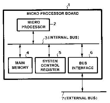
Une carte à microprocesseur d'un système de surveillance de bus comprenant un bus interne qui comprend un microprocesseur, des lignes d'adresse, des lignes de données et des lignes de signal de commande, une mémoire connectée par l'intermédiaire du bus interne avec des registres de microprocesseur, comme un registre de commande de système et un circuit d'interface de bus. L'accès à la mémoire principale, au registre ou à l'interface de bus qui est exécuté par le microprocesseur est envoyé à un bus externe par l'intermédiaire du circuit d'interface de bus. Ainsi, l'état de fonctionnement du microprocesseur ou du bus interne peut être surveillé par la surveillance du bus externe.


Abrégé anglais

A microprocessor board of a bus monitoring system comprises an internal bus which comprise a microprocessor, address lines, data lines, and control signal lines, a memory connected via the internal bus with microprocessor registers, such as a system control register, and a bus interface circuit. The access to the main memory, the register, or the bus interface which is executed by the microprocessor is outputted to an external bus via the bus interface circuit. Thus, the operation status of the microprocessor or the internal bus can be monitored by monitoring the external bus.

Revendications

Note : Les revendications sont présentées dans la langue officielle dans laquelle elles ont été soumises.


CLAIMS:
1. A bus monitoring system which comprises:
a microprocessor;
an internal bus comprising address lines, data
lines and control signal lines;
a main memory which is connected to said
microprocessor via said internal bus;
a system control register which is connected to
said microprocessor via said internal bus;
a bus interface which is connected to said
microprocessor via said internal bus;
an external bus which is connected to said
internal bus via said bus interface;
wherein said bus interface outputs the same signal
as the signal on said address lines to first lines of said
external bus and the same signal as the signal on said data
lines to second lines of said external bus, said first lines
being different from said second lines, and
wherein said bus interface outputs an address
strobe signal which indicates whether or not signals on said
address lines are valid and a data ready signal which
indicates whether or not signals on said data lines are
valid, and
wherein said data ready signal is a detection
signal of a negative edge of a CAS signal.
2. The bus monitoring system according to claim 1,
wherein said microprocessor, said internal bus, said main
7

memory, said system control register, and said bus interface
are mounted on a printed-circuit board substrate.
3. The bus monitoring system according to claim 1,
wherein said microprocessor, said internal bus, said main
memory, said system control register, and said bus interface
are mounted on a semiconductor substrate.
8

Description

Note : Les descriptions sont présentées dans la langue officielle dans laquelle elles ont été soumises.


CA 02254525 2002-05-15
74935-19
BUS MONITORING SYSTEM
BACKGROUND OF THE INVENTION
1. Field of the Invention
The present invention relates to a bus monitoring
system and particularly, to a bus monitoring system for
monitoring the operation status of a microprocessor.
2. Description of the Prior Art
There is disclosed a multi-chip module evaluating
device in, for example, Japanese Patent Laid-Open No. 5-
120160 (1993), which monitors signals on wires of a multi-
chip module between a floating operation unit and a data
memory. The signals on the wires which are embedded in the
module substrate of a multi-chip module are monitored by
connecting, via a probe, a leader pad on the module
substrate with a monitor unit which comprises a memory, an
address generator, and a comparator. This evaluating device
can monitor directly the signals on the wires, without using
any test element group (TEG). Therefore, this evaluating
device is employed for monitoring the signals on the wires,
because an evaluation using only signals extracted to
external pins is not sufficient, in case of large scale
integration (LSI) packages mounted on the module substrate.
In this connection, the above-mentioned
conventional device has the following disadvantages:
Firstly, leader pads are necessary for monitoring
the signals on the wires because the signals on the wires
are imbedded in the module substrate. Accordingly, the
above-mentioned evaluating device is not of any use for a
small sized multi-chip module, because the number of pads
increases with the increase in the number of wires in the
1

CA 02254525 2005-02-03
74935-19
module substrate, which results in the increase in the area
required for pads.
Secondly, a testing device is necessary
exclusively for bus monitoring. Specially designed probes
are required for connection to the special leader pads on
the module substrate.
Thirdly, the reliability of bus monitoring is
lowered. When the leader pads are inferior due to a
manufacturing process, then the module substrate can not be
monitored completely.
SUMMARY OF THE INVENTION
Therefore, an object of the present invention is
to provide a bus monitoring system with improved reliability
for monitoring easily the bus of a microprocessor via bus
interface, when evaluating bus interface peripheral circuits
and the software for a microprocessor board. Another object
of the present invention is to improve the reliability of
the evaluation system.
According to the present invention, there is
provided a bus monitoring system which comprises: a
microprocessor; an internal bus comprising address lines,
data lines and control signal lines; a main memory which is
connected to said microprocessor via said internal bus; a
system control register which is connected to said
microprocessor via said internal bus; a bus interface which
is connected to said microprocessor via said internal bus;
an external bus which is connected to said internal bus via
said bus interface; wherein said bus interface outputs the
same signal as the signal on said address lines to first
lines of said external bus and the same signal as the signal
on said data lines to second lines of said external bus,
2

CA 02254525 2007-01-11
74935-19
said first lines being different from said second lines, and
wherein said bus interface outputs an address strobe signal
which indicates whether or not signals on said address lines
are valid and a data ready signal which indicates whether or
not signals on said data lines are valid, and wherein said
data ready signal is a detection signal of a negative edge
of a CAS signal.
2a

CA 02254525 2004-02-09
74935-19
In the bus monitoring system, the bus interface
may output an address strobe signal which indicates whether
or not signals on the address lines are valid and a data
ready signal which indicates whether or not signals on the
data lines are valid.
According to the present invention as explained
above, the following effects are obtained:
Firstly, the leader pads become unnecessary for
monitoring the signals on the wires which are imbedded in a
module substrate, because every status of an internal bus
can be monitored via the bus interface.
Secondly, a high density mounting board such as a
multi-chip module can be furthermore integrated in a higher
density system, while keeping the capability of the internal
bus monitoring, because the leader pads become unnecessary
and the wide mounting area for other purposes is preserved.
Thirdly, bus monitoring becomes easy, because
ordinary available instruments can be used for bus
monitoring at the external bus connected with bus interface,
or the peripheral circuit of a microprocessor board.
BRIEF EXPLANATION OF THE DRAWINGS
Figure 1 is a block diagram of a bus monitoring
system of an embodiment of the present invention.
Figure 2 is a timing chart for explaining the
action of the bus monitoring system of an embodiment of the
present invention.
3

CA 02254525 2002-05-15
74935-19
PREFERRED EMBODIMENT OF THE INVENTION
A preferred embodiment of the present invention is
explained. The microprocessor board of the bus monitoring
system of the present invention comprises an internal bus
which comprise a microprocessor, address lines, data lines,
and control signal lines, a main memory connected via the
internal bus with the microprocessor, registers such as a
system control register, and a bus interface circuit. Every
access to the main memory, the system control register, and
the bus interface by the microprocessor is outputted to an
external bus via the bus interface circuit. Accordingly,
the operation status of the microprocessor or the internal
bus can be monitored by monitoring the external bus.
Referring to the accompanying drawings, a working
example of the present invention is explained to clarify the
embodiment of the present invention.
As shown in Figure 1, a microprocessor board 1
comprises a microprocessor 2 connected with an internal bus
3, a main memory 4, a system control register 5 and a bus
interface 6. Further, the microprocessor board 1 is
connected with an external bus 7 via the bus interface 6.
Next, referring to Figure 1, the action of the
microprocessor board 1 of the working example is explained.
The microprocessor 2 accesses the main memory 4
and the system control register 5 via the internal bus 3.
Therefore, every access in the microprocessor board 1 can be
monitored by monitoring the internal bus 3.
The bus interface 6 outputs addresses, data, and
control signals from the internal bus 3 to the external bus
4

CA 02254525 2002-05-15
74935-19
7, when the microprocessor 2 executes a write access to main
memory 4, or the system control register 5.
Also, the bus interface 6 outputs addresses, data,
and control signals from the internal bus 3 to the external
bus 7, when the microprocessor 2 executes a read access to
the main memory 4, or the system control register 5.
Thus, the internal bus 3 can be monitored by
monitoring the external bus 7. In other words, the
execution process of a program of the microprocessor 2
mounted on the microprocessor board 1 can be traced by
monitoring the external bus 7 since all address, data and
control signals on the internal bus 3 are output to the
external bus 7.
Referring to Figure 2, the action of the bus
interface 6 between the internal bus 3 and the external bus
7 of the working example is explained.
The action of a two word write into main memory 4
by the microprocessor 2 shown in Figure 1, is shown
concretely in Figure 2.
The internal bus 3 executes a write access to the
main memory 4, carrying an internal bus address 10 and an
internal bus write data 11 in the microprocessor 2.
The main memory 4 accepts the internal bus address
10 and the internal bus write data 11 and writes them by
using a row address strobe (RAS) control signal 12 and a
column address strobe (CAS) control signal 13, while the bus
interface 6 outputs the same address as the internal bus
address 10 as an external bus address 14. At the same time,
the bus interface 6 outputs an external bus strobe 15 to
validate the external bus address 14.
5

CA 02254525 2002-05-15
74935-19
The bus interface 6 outputs an external bus data
16 which is the same as an internal bus data 11. At the
same time, the bus interface 6 outputs an external bus data
ready 17 synchronized with the CAS control signal 13.
Thus, an effective timing of a write address and
write data are confirmed by the external bus 7, when the
microprocessor 2 executes a write access to the main memory
4.
Similarly, an effective timing of a read address
and read data are confirmed by the external bus 7, when the
microprocessor 2 executes a read access to the main memory
4. The accesses to the system control register 5 are
confirmed similarly. Thus, the internal bus 3 can be
monitored by the external bus 7.
6

Dessin représentatif
Une figure unique qui représente un dessin illustrant l'invention.
États administratifs

2024-08-01 : Dans le cadre de la transition vers les Brevets de nouvelle génération (BNG), la base de données sur les brevets canadiens (BDBC) contient désormais un Historique d'événement plus détaillé, qui reproduit le Journal des événements de notre nouvelle solution interne.

Veuillez noter que les événements débutant par « Inactive : » se réfèrent à des événements qui ne sont plus utilisés dans notre nouvelle solution interne.

Pour une meilleure compréhension de l'état de la demande ou brevet qui figure sur cette page, la rubrique Mise en garde , et les descriptions de Brevet , Historique d'événement , Taxes périodiques et Historique des paiements devraient être consultées.

Historique d'événement

Description Date
Le délai pour l'annulation est expiré 2013-11-26
Lettre envoyée 2012-11-26
Accordé par délivrance 2008-11-04
Inactive : Page couverture publiée 2008-11-03
Inactive : Taxe finale reçue 2008-08-11
Préoctroi 2008-08-11
Un avis d'acceptation est envoyé 2008-02-14
Lettre envoyée 2008-02-14
Un avis d'acceptation est envoyé 2008-02-14
Inactive : Pages reçues à l'acceptation 2008-01-08
Inactive : Lettre officielle 2007-12-05
Inactive : CIB attribuée 2007-09-04
Inactive : CIB enlevée 2007-09-04
Inactive : CIB en 1re position 2007-09-04
Inactive : CIB attribuée 2007-09-04
Inactive : Approuvée aux fins d'acceptation (AFA) 2007-08-24
Modification reçue - modification volontaire 2007-01-11
Inactive : Dem. de l'examinateur par.30(2) Règles 2006-10-02
Modification reçue - modification volontaire 2006-03-28
Inactive : CIB de MCD 2006-03-12
Inactive : Dem. de l'examinateur par.30(2) Règles 2005-10-05
Modification reçue - modification volontaire 2005-02-03
Inactive : Dem. de l'examinateur par.30(2) Règles 2004-08-03
Modification reçue - modification volontaire 2004-04-08
Modification reçue - modification volontaire 2004-02-09
Inactive : Dem. de l'examinateur par.30(2) Règles 2003-08-08
Modification reçue - modification volontaire 2002-05-15
Inactive : Dem. de l'examinateur par.30(2) Règles 2002-02-11
Inactive : Page couverture publiée 1999-06-17
Demande publiée (accessible au public) 1999-05-28
Inactive : CIB en 1re position 1999-01-22
Symbole de classement modifié 1999-01-22
Inactive : CIB attribuée 1999-01-22
Inactive : Certificat de dépôt - RE (Anglais) 1999-01-07
Demande reçue - nationale ordinaire 1999-01-06
Exigences pour une requête d'examen - jugée conforme 1998-11-25
Toutes les exigences pour l'examen - jugée conforme 1998-11-25

Historique d'abandonnement

Il n'y a pas d'historique d'abandonnement

Taxes périodiques

Le dernier paiement a été reçu le 2008-10-02

Avis : Si le paiement en totalité n'a pas été reçu au plus tard à la date indiquée, une taxe supplémentaire peut être imposée, soit une des taxes suivantes :

  • taxe de rétablissement ;
  • taxe pour paiement en souffrance ; ou
  • taxe additionnelle pour le renversement d'une péremption réputée.

Les taxes sur les brevets sont ajustées au 1er janvier de chaque année. Les montants ci-dessus sont les montants actuels s'ils sont reçus au plus tard le 31 décembre de l'année en cours.
Veuillez vous référer à la page web des taxes sur les brevets de l'OPIC pour voir tous les montants actuels des taxes.

Historique des taxes

Type de taxes Anniversaire Échéance Date payée
Requête d'examen - générale 1998-11-25
Taxe pour le dépôt - générale 1998-11-25
Enregistrement d'un document 1998-11-25
TM (demande, 2e anniv.) - générale 02 2000-11-27 2000-09-28
TM (demande, 3e anniv.) - générale 03 2001-11-26 2001-09-28
TM (demande, 4e anniv.) - générale 04 2002-11-25 2002-10-08
TM (demande, 5e anniv.) - générale 05 2003-11-25 2003-09-11
TM (demande, 6e anniv.) - générale 06 2004-11-25 2004-09-16
TM (demande, 7e anniv.) - générale 07 2005-11-25 2005-09-16
TM (demande, 8e anniv.) - générale 08 2006-11-27 2006-09-19
TM (demande, 9e anniv.) - générale 09 2007-11-26 2007-10-09
Taxe finale - générale 2008-08-11
TM (demande, 10e anniv.) - générale 10 2008-11-25 2008-10-02
TM (brevet, 11e anniv.) - générale 2009-11-25 2009-10-14
TM (brevet, 12e anniv.) - générale 2010-11-25 2010-10-25
TM (brevet, 13e anniv.) - générale 2011-11-25 2011-10-13
Titulaires au dossier

Les titulaires actuels et antérieures au dossier sont affichés en ordre alphabétique.

Titulaires actuels au dossier
NEC CORPORATION
Titulaires antérieures au dossier
HIROFUMI SUDO
Les propriétaires antérieurs qui ne figurent pas dans la liste des « Propriétaires au dossier » apparaîtront dans d'autres documents au dossier.
Documents

Pour visionner les fichiers sélectionnés, entrer le code reCAPTCHA :


Pour visualiser une image, cliquer sur un lien dans la colonne description du document. Pour télécharger l'image (les images), cliquer l'une ou plusieurs cases à cocher dans la première colonne et ensuite cliquer sur le bouton "Télécharger sélection en format PDF (archive Zip)" ou le bouton "Télécharger sélection (en un fichier PDF fusionné)".

Liste des documents de brevet publiés et non publiés sur la BDBC .

Si vous avez des difficultés à accéder au contenu, veuillez communiquer avec le Centre de services à la clientèle au 1-866-997-1936, ou envoyer un courriel au Centre de service à la clientèle de l'OPIC.


Description du
Document 
Date
(aaaa-mm-jj) 
Nombre de pages   Taille de l'image (Ko) 
Dessin représentatif 1999-06-15 1 7
Abrégé 1998-11-24 1 20
Description 1998-11-24 6 242
Dessins 1998-11-24 2 28
Revendications 1998-11-24 2 65
Abrégé 2002-05-14 1 18
Description 2002-05-14 6 240
Revendications 2002-05-14 1 33
Description 2004-02-08 7 238
Revendications 2004-02-08 1 26
Revendications 2005-02-02 1 30
Description 2005-02-02 7 239
Description 2006-03-27 7 241
Revendications 2006-03-27 2 41
Description 2007-01-10 7 241
Revendications 2007-01-10 2 42
Dessin représentatif 2008-10-15 1 8
Courtoisie - Certificat d'enregistrement (document(s) connexe(s)) 1999-01-11 1 114
Certificat de dépôt (anglais) 1999-01-06 1 163
Rappel de taxe de maintien due 2000-07-25 1 109
Avis du commissaire - Demande jugée acceptable 2008-02-13 1 164
Avis concernant la taxe de maintien 2013-01-06 1 170
Correspondance 2008-01-07 1 41
Correspondance 2008-08-10 1 39