Note : Les descriptions sont présentées dans la langue officielle dans laquelle elles ont été soumises.
WG 97/48992 PCTlUS97/09853
PLASTIC ARTICLES HAVING MULTI-LAYER P.NTIREFLECTION
COATINGS, AND SOL-GEL PROCESS FOR DEPOSITING SUCH COATINGS
BACKGROUND OF THE INVENTION
This invention relates generally to antireflection
coatings on plastic substrates and, more particularly, to sol-gel
processes that deposit mufti-layer antireflection coatings of
silicon dioxide and titanium dioxide.
Antireflection coatings for plastic substrates reduce
the reflectance of visible light from the substrates and enhance
the transmission of such J.ight into, or through, the substrates.
When the substrates are used as cover plates for display
instruments, these coatings enhance the brightness, contrast and
readability of the displayed information, for a variety of
lighting conditions.
Some antireflection coatin:3s of this kind have included
mufti-layer stacks having alternate layers of titanium dioxide
and silicon dioxide. The titanium dioxide layers generally have
a relatively high refractive :index, and the silicon dioxide
layers generally have a relatively low refractive index,
typically lower than even that of the underlying plastic
substrate. Each layer o~ the mufti-layer stack has a prescribed
thickness, and reflections from multiple layers interfere
destructively to result ire reduced reflectivity over the entire
visible spectrum o. 400 to 700 manometers.
Although various antireflection coatings, including the
mufti-layer coatings described brief-wy above, have been generally
effective in providing reduced reflectivity over the visible
spectrum, the coatings are not considered to be entirely
satisfactory for use in many applications. For example, some of
the processes provide coatings tha;_ are highly susceptible to
mechanical damage from abrasion and that exhibit poor adhesion to
the underlying substrate.
Moreover, processes fog depositing such coatings,
inciud-.~na electron beam deposition, reactive plasma sputtering,
CA 02257297 2001-10-02
WO 97/48992 PCT/US97/U9853
and ion-assisted deposition, are relatively expens,wve to
implement and are not readily usable for coating substrates
:having many sizes and configura~;~ons. :In addition, some
substrates can be damaged by such processes, because of excessive
heat generation. Substrates formed of polymethyl methac rylate
(PMMA), polystyrene, polycarbonate, all.yl digiycol carbonate (CR-
39) , and polyethylene t:.erephthalate (PET) are considered to be
particularly susceptible to such heat damage. Some deposition
processes have eliminated the occurrence of heat damage, but they
are believed to be suitable for use only with substrates of
limited sizes and shapes; such as eyewear lenses.
It should, tr~:erefore, be appreciated that there is a
need for an improved mufti-layer antireflection coating and
process for depositing such coatings on plastic substrates in a
variety of sizes and configuratior..s, with reduced expense and
with reduced susceptibility to mechanical, environmental and heat
damage. The present invention fulfills this reed.
SUMMARY OF THE INVENTION
In a first broad aspect the present invention resides in
a mufti-layer antireflection coating, and a process for depositing
a mufti-layer antireflection coating on a plastic substrate, the
coating having high mechanical strength and durability. The
process includes steps of preparing one or more first polymerized
solutions consisting essentially of a first non-organic alkoxide,
an alcohol, and water, wherein the or_e or more first polymerized
solutions are formulated to provide thin films having a refractive
index of 1.80 or more; preparing one or more second polymerized
solutions consisting essentially of a second non-organic a.lkoxide,
an alcohol, and water, wherein the one or more second polymerized
solutions are formulated to provi de t~~in f i lms having a refractive
index of 1.46 or less, and wherein the second alkoxide is
different from the first alkoxide; applying a first polymerized
solution and a second pc>lymeria.ed solution to the plastic
J5 substrate, or tc a previous~~.y applied coating layer, in an
CA 02257297 2001-10-02
2A
alternating fashion, wherev~n a prescribed amount of the solution
adheres to the subsr_rat~e fo~ilowing each step of applying; and
~:ollowing each step of app=_yirg, curing the adhered sol ution, before
t;he next successive step ~z applying occurs, each such step of curing
~_orming a separate, polymerized layer on the substrate, wherein the
:successive polymerized layers cooperate to form a mufti-layer coating
of at least :COUr layers that provides substantially reduced
reflectivity of visible .Light.
In a second broad aspect the invention consists of a coated
article comprising a plastic; substrate; and an antireflection coating
deposited on the plastic substrate; wherein the coating includes four
or more polymerized layen:~ of prescribed uniform thickness, the
=_ayers alternating betwE~en layers consisting essentially ofi
polymerized titanium dioxide and lagers consisting essentially of
polymerized silicon dioxide; and wherein the layers cooperate to
provide substantially reduced reflectivity of visible light.
In a further aspect, the invention resides in a mufti-layer
antireflection coating, and a process for depositing such coatings on
a plastic substrate, the coating having high mechanical strength and
durability. The process, includes preliminary steps of mixing
together an alkoxide, an alcohol, and water to produce one or more
l:irst polymerized solutions and to produce one or more second
polymerized solutions, wherein the first solutions are formulated to
provide thin films having a refractive index of 1.80 or more and the
second solutions are formulated to provide thin films having a
~:efractive index of 1.46 or less. A first polymerized solution and
~~ second polymerized solution are applied to a plastic substrate in
an alternating fashion, each such application causing a prescribed
amount of the solution to adhere to the substrate. Following the
each step of applying, the adhered solution is cured, to form a
separate, polymerized lawyer on the substrate. The successive
polymerized layers cooperate to form a mufti-layer coating of at
CA 02257297 2001-10-02
WO 97/48992 PCT/LTS97/09853
3
least four layers hat provide s substantially reduced
reflectively of visible light.
The one or more first solutions preferably are produced
by mixing a titanium alkoxide such as titanium isopropoxide,
titanium propoxide, or titanium ethoxide with ethyl alcohol,
deionized water, and an acidic catalyst such as hydrochloric acid
or nitric acid, in prescribed relata.ve proportions. The one or
more second solutions preferably are produced by mixing a silicon
alkoxide such as tetraethyl orthosilicate or tetramethyl
orthosilicate, ethyl alcohol, deionized water, and an acidic
catalyst such as hydrochloric acAd or nitric acid, in prescribed
relative proportions. When cured, the sclutions produce
-:, polymerized, solid layers of titanium dioxide and silicon
dioxide. The titanium dioxide layers have an index of refraction
in the range of 1.80 to 2.20, and the silicon dioxide layers have
a refractive index in the range of 1.40 to 1.40. In the case of
a four-layer coating, t:he first layer preferably is titanium
dioxide, with a unifcrm thickness in the range of 10 to 30
nanometers (nm), the second layer is silicon dioxide, with a
uniform thickness in the range of 20 to 40 nm, the third layer is
titanium dioxide, with a uniform thickness in the range of 70 to
100 nm, and the fourth layer is silicon dioxide, with a uniform
thickness in the range of 80 to 110 nm.
The first and second solutior_s are each mixed for at
least four hours, during whicr: time the solutions undergo
hydrolysis reactions and polymerization. Before application to
the substrate, the solutions are filtered through a filter having
openings no larger trlan 5 microns in size.
The step of app,;y~~ng the coating occurs within a
chamber in which the humid=t-r~ is carefully controlled. When a
titar:ium dioxide layer is being applied, the humidity preferably
is mair~tained above 400, while when a silicon. dioxide layer is
beir_g applied, the humidity i.s maintained below 40~. All four
layers are cured at an eie~,rated temperature !e. g,, 84°C for some
33 grades of polyznethyl metr:acrylate', fcr at 'yeas' 10 minutes each.
CA 02257297 2001-10-02
WO 97/48992 PCT/US97/Q9$53
4
To avoid thermal shock, the temperature is controllably raised to
the cure temperature at a rate not exceeding 15°C per minute and,
after curing, lowered back to room temperature at a similar rate.
In some cases, a thin base coat is applied to the
plastic substrate, before the layers of the antireflE~ction
coating. This base coat minimizes the visibility of any fine
scratches in the substrate's surface.
The coated plastic substrate produced by the process of
the invention exhibits an average reflectance of less than 0.20
over the wavelength range of of 450 to 650 nm and less than 0.90
over the entire visible spectrum of 400 to 700 nm. The coating
°_xhibits excellent abrasion resistance and adhesion to the
underlying substrate. In addition, the coating can withstand
severe environmental conditions without noticeable degradation cf
its optical and mechanical properties. Suitable sub~~trate
materials include po"~~znethyl methacrylate, polystyrene,
polycarbonate, allyl dic~lycoi carbonate, and polyethylene
rerephthalate.
Other features and advantages of the present invention
;should become apparent from the following description of the
~~referred process, taken in conjunction with the accompanying
drawings, which illustrate, by way o= example, the principles of
l~he invention.
~3RIEF DESCRIPTION OF THE DRAWINGS
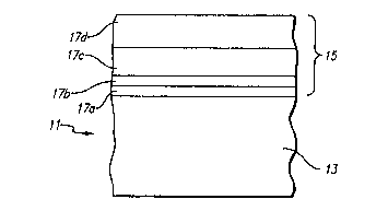
2~; FIG. 1 is a cross-sectional view, not to scale, of a
transparent plastic substrate on which has been deposited a four-
:'~ayer antireflectiom coa-:ing using t:~e preferred process of the
:invention.
FI~3. 2 is a graph of the reflectivity of a polvmethyl
rrethacrylate substrate, both with anti wit:nout a mufti-layer
antireflection coating depe~~sited ~_. a.~_cJordance with the preferred
i~rocess of the invention.
CA 02257297 2001-10-02
CA 02257297 1998-12-04
WO 97/48992 PCT/US97/09853
DESCRIPTION OF THE PREFERRED EMBODIMENT AND PROCESS
With reference now to the drawings, and particularly to
FIG. 1, there is shown a panel 11 that includes a plastic
substrate 13 on which is deposited a four-layer antireflection
5 coating 15, for providing low reflectivity over the entire
visible spectrum of 400 to 700 nanometers (nm). The
antireflection coating includes alternating layers of polymerized
titanium dioxide and polymerized silicon dioxide, which are
deposited successively using a sol-gel process by which each
l0 layer's thickness and index of refraction can be carefully
controlled. The first layer 17a and third layer 17c of the
coating are formed of titanium dioxide, and the second layer 17b
and fourth layer 17d of the coating are formed of silicon
dioxide. The substrate 13 can be formed of any conventional
plastic material such as polymethyl methacrylate (PMMA),
polystyrene, polycarbonate, allyl diglycol carbonate (CR-39), or
polyethylene terephthalate (PET).
In a preliminary step of the process, the plastic
substrate 13 is cleaned. Plastic substrates in the form of flat
sheets usually are supplied by manufacturers with an adhesive
paper on both surfaces, to minimize damage from handling. This
adhesive paper is first peeled off, and the bare sheet is then
cleaned in an ultrasonic bath with detergent solutions and rinsed
with deionized water. The cleaned sheet is then dried under a
hot air flow, followed by an ionized air flow, to avoid a static
charge buildup on the surface. The plastic sheets used in the
examples set forth below were rectangular and flat, with
dimensions of 15 cm x 40 cm x 2 mm. However, the process
disclosed can readily be used for sheets having either smaller or
larger sizes, and for complicated shapes having curvatures and
bends.
The antireflection coating 15 sometimes can make fine
scratches in the surface of the substrate 13 unduly visible. It
is therefore sometimes desirable to apply a thin, silicon- or
acrylic-based base coat to the substrate surface. The base coat
CA 02257297 1998-12-04
WO 97/48992 , PCT/US97/09853
6
preferably has an index of refraction comparable to that of the
underlying plastic substrate, and it is applied, e.g., by dip
coating, in a thickness of about 1 to 5 microns. A suitable UV-
curable coating material is UVB510R6, available from Red Spot
Paint & Varnish Co., Inc., of Evansville, Indiana. A suitable
thermally cured material is Silvue 201, available from SDC
Coatings Inc., of Anaheim, California.
The coating solutions for depositing the titanium
dioxide layers, i . a . , the first layer 17a and the third layer
17c, are prepared by mixing titanium isopropoxide ((Ti(OiPr)4),
ethyl alcohol (EtOH), deionized water (H z0), and hydrochloric
acid (HC1). The general range of the molar composition
considered to be suitable for the first layer is 1 mole of
Ti(OiPr)4, 80 to 120 moles of EtOH, 2 to 5 moles of H20, and 0.05
to 0.5 mole of HCl. The general range of the molar composition
considered to be suitable for the third layer is 1 mole of
Ti(OiPr)4, 35 to 55 moles of EtOH, 2 to 5 moles of H O, and 0.1
to 0.4 mole of HCl. Other titanium alkoxides, e.g., titanium
propoxide and titanium ethoxide, can be substituted for titanium
isopropoxide. In addition, nitric acid (HN03) can be substituted
for hydrochloric acid. The mole ratio between titanium
isopropoxide and ethyl alcohol was found to be important in
maintaining the stability of the solution for 90 days or more,
for continuous use.
The four components of the titanium dioxide solutions
are mixed at room temperature for at least four hours, during
which time the solutions undergo hydrolysis and polymerization.
The polymerized solutions then are filtered and transferred to
suitable coating tanks. The coating tanks preferably are made of
polypropylene, and they are thoroughly cleaned before receiving
the solutions.
The coating solutions for depositing the silicon
dioxide layers, i.e., the second layer 17b and the fourth layer
17d, are prepared by mixing tetraethyl orthosilicate (TEOS),
ethyl alcohol (EtOH), deionized water (H20), and hydrochloric
CA 02257297 1998-12-04
WO 97/48992 PCT/US97/09853
7
acid (HCl). The general range of the molar composition
considered to be suitable for the second layer is 1 mole of TEOS,
70 to 110 moles of EtOH, 2 to 6 moles of H20, and 0.1 to 0.3 mole
of HC1. The general range of suitable molar composition
considered to be suitable for the fourth layer is 1 mole of TEOS,
20 to 40 moles of EtOH, 2 to 5 moles of deionized H20, and 0.05
to 0.1 mole of HC1. Other silicon alkoxides, such as tetramethyl
orthosilicate, can be substituted for tetraethyl orthosilicate,
and nitric acid (HN03) can be substituted for hydrochloric acid.
The mole ratio between tetraethyl orthosilicate and ethyl alcohol
was found to be important in maintaining the stability of the
solution for 30 days or more, for repetitive coatings.
The four components of the silicon dioxide solutions
are mixed for at least four hours, all at room temperature,
during which time the solutions undergo hydrolysis and
polymerization. The solutions then are filtered and transferred
to suitable polypropylene coating tanks.
The prepared titanium dioxide and silicon dioxide
solutions are deposited as individual layers on the plastic
substrate 13 by any of a number of suitable techniques, but
preferably by dip coating. In the dip coating technique, the
substrate is clamped to a cantilevered arm, and a drive system
moves the arm and substrate down and up along a vertical axis.
The range of motion must be sufficient to dip the substrate fully
into, and out of, a dip tank that carries the solution.
Each successive layer of the multi-layer antireflection
coating 15 is deposited on the substrate 13 by lowering the
cantilevered arm and substrate at a predetermined speed into the
dip tank carrying the solution. After remaining submerged for a
brief time period, the substrate is withdrawn from the solution
at a predetermined speed. The drive system includes a suitably
programmed computer, for precisely controlling the withdrawal
speed of the arm and substrate, so as to control the thickness of
the layer being deposited. In general, slower withdrawal speeds
yield thinner coating layers.
CA 02257297 1998-12-04
WO 97/48992 PCT/US97/09853
8
The dip tank and cantilevered arm are enclosed within
a dip coating chamber having a controlled humidity. It has been
found that the humidity within the chamber must be precisely
controlled, to ensure the depositing of transparent, defect-free
coating layers. For depositing titanium dioxide layers (e. g.,
the layers 17a and 17c), the relative humidity within the chamber
is controlled to be in the range of 40 to 800. A lower humidity
can cause the deposited layer to be translucent or even opaque,
and a higher humidity can cause the deposited layer to include
spot defects. For depositing silicon dioxide layers (e.g., the
layers 17b and 17d), on the other hand, the relative humidity
within the chamber is controlled to be in the range of 20 to 40%.
A higher humidity can cause spot defects in the deposited layer.
Maintaining the humidity within the dip coating chamber
at a value within the prescribed range yields clear, defect-free
coating layers on the specified plastic substrate 13. The
temperature within the chamber preferably is maintained in the
range of 19° to 25°C.
Following the depositing of each coating layer, the
panel 11 is transferred to an oven, for curing. Curing
evaporates residual organics from the uppermost layer, to yield
a solid film with some residual porosity. The temperature of the
oven is controlled according to the type of substrate 13 used,
and it preferably is selected to be the maximum temperature that
the particular substrate can withstand without deformation. For
PMMA, the cure temperature is maintained at 84°C.
The duration of the cure for each coating layer affects
the strength of the resulting multi-layer stack 15. In the
preferred process, the cure duration for each of the layers 17a,
17b, 17c and 17d is at least 10 minutes. Shorter cure durations
for any one of the four layers can weaken the mechanical
properties of the entire multi-layer coating 15, including either
or both of its scratch resistance and adhesion.
CA 02257297 1998-12-04
WO 97/48992 PCT/US97/09853
9
To avoid a thermal shock to the coated substrate 13
when it is first placed into the curing oven, the oven's
temperature is initially maintained at about 23°C and then raised
at a controlled, uniform rate to its final 84°C temperature.
This temperature rise preferably occurs at a rate not exceeding
15°C per minute. After maintenance at this 84°C temperature for
the specified cure duration, e.g., 10 minutes, the oven
temperature is cooled to 23°C, again at a controlled, uniform
rate of 15°C per minute or less. A failure to avoid a thermal
shock can lead to the formation of cracks in the deposited layer.
Following the curing of the fourth layer 17d of the
antireflection coating 15, the panel 11 is subjected to several
tests. One test is made using a spectrophotometer, to ascertain
the coated substrate's reflectance over the visible wavelength
range of 400 to 700 nm. Other tests ascertain the coating's
mechanical strength, including a pencil scratch test and a tape
adhesion test.
In the pencil scratch test, standard lead pencils
having ratings of HB, H, 2H, 3H, etc . are each sharpened to a
fine lead tip and dragged several millimeters along the surface
of the antireflection coating 15, while under a 1000 gram
compressive load. The coating then is inspected for the presence
of any visual scratch marks, under standard room lighting
conditions.
In the tape adhesion test, a strip of 3M-brand
transparent tape is firmly pressed against the antireflection
coating 15 and then removed vertically with a quick upward pull.
The coating surface then is inspected for uniformity.
The susceptibility of the coated substrate 13 to
environmental degradation also is tested. These tests include:
1) a high temperature test, 2) a low temperature test, 3) a
humidity test, 4) a thermal shock test, and 5) a chemical
resistance test.
CA 02257297 1998-12-04
WO 97/48992 PCT/US97/09853
In the high temperature test, the panel 11 is exposed
to 84°C for 192 hours, after which it is inspected for any
degradation in its reflectance, scratch resistance, adhesion
properties, and visual appearance. In the low temperature test,
5 the coated substrate is exposed to -40°C for 192 hours, after
which these same parameters are checked. In the humidity test,
the coated substrate is exposed to 95o relative humidity at 60°C,
for 192 hours, and the same parameters are then checked. In the
thermal shock test, the coated substrate is cycled 200 times
10 between 84°C and -30°C, and the same parameters are then
checked.
Finally, in the chemical resistance test, a detergent, a
polishing wax, brake oil, and a household glass cleaner are
applied to the coating 15, and the panel 11 is exposed to 60°C
for 24 hours, after which the same parameters are checked.
The preferred process of the invention having been
generally described, the following particular examples will
illustrate various properties of the invention and demonstrate
the practical advantages of the invention. These examples should
be construed merely as illustrative, and should not limit the
remainder of the disclosure or the claims.
EXAMPLE 1
This example produced a four-layer antireflection
coating on a polymethyl methacrylate (PMMA) substrate having a
length of 40 cm, a width of 15 cm, and a thickness of 2 mm.
Adhesive paper was first removed from the PMMA sheet, and the
bare sheet was then cleaned in an ultrasonic bath with detergent
solutions and thoroughly rinsed with deionized water. The sheet
was then dried under a hot air flow, followed by an ionized air
flow, to avoid static charge buildup.
Separate coating solutions were prepared for each of
the coating's four layers. The solutions for the first and third
layers were titanium based, while the solutions for the second
and fourth layers were silicon based.
CA 02257297 1998-12-04
WO 97/48992 PCT/US97/09853
11
The solution for the first layer was prepared by mixing
titanium isopropoxide (Ti(OiPr)4), ethyl alcohol (EtOH),
deionized water (Hz0), and hydrochloric acid (HCl). The
composition for this first layer was Ti(OiPr)4 . EtOH . Hz0 . HCl
- 1 . 108 . 3 . 0.2. These four components were mixed thoroughly
at room temperature for four hours, after which the solution was
allowed to stand at room temperature for 48 hours. During this
time the solution underwent an hydrolysis reaction and
polymerization, to form a titanium dioxide polymer solution. The
polymerized solution then was filtered and transferred to a
polypropylene storage tank.
The solution for the first layer was transferred to a
dip coating chamber, and the PMMA substrate was clamped to a
vertically movable arm. The temperature within the chamber was
controlled to be 23°C, and the humidity within the chamber was
controlled to be in the range of 40 to 80%. The substrate then
was lowered into the solution and kept submerged for 10 seconds,
after which it was withdrawn at a speed of 0.2 cm per second. As
the substrate was withdrawn, a clear, uniform layer was obtained.
The substrate coated with the first layer then was
transferred to an oven, and the temperature of the oven was
raised at a uniform rate 2°C per minute, from 23°C to
84°C. This
84°C temperature was maintained for ten minutes, during which
time the first coating layer was fully cured. The oven
temperature then was lowered back to 23°C, again at a uniform
rate of 2°C per minute, and the substrate was removed. The
thickness of the cured titanium dioxide first layer was measured
in the range of 15 to 25 nm, and the layer's refractive index was
measured to be 2.00 at a wavelength of 550 nm.
The coating solution for the second layer was prepared
by mixing tetraethyl orthosilicate (TEOS), ethyl alcohol (EtOH),
deionized water (H20), and hydrochloric acid (HCl). The
composition for this second layer was TEOS . EtOH . H20 . HC1 =
1 . 80 . 3 . 0.2. These four components were mixed thoroughly at
room temperature for four hours, after which the solution was
CA 02257297 1998-12-04
WO 97/48992 PCT/US97/09853
12
allowed to stand at room temperature for another four hours.
During this time the solution underwent an hydrolysis reaction
and polymerization, to form a silicon dioxide polymer solution.
The polymerized solution then was filtered and transferred to a
polypropylene storage tank.
The solution for the second layer .was transferred to
the dip coating chamber, and the PMMA substrate, with the first
layer of the four-layer antireflection coating already adhered,
was clamped to the vertically movable arm. The temperature
within the chamber was controlled to be 23°C, and the humidity
within the chamber was controlled to be within the range of 20 to
400. The substrate then was lowered into the solution and kept
submerged for 10 seconds, after which it was withdrawn at a speed
of 0.12 cm per second. As the substrate was withdrawn, a clear,
uniform second layer was obtained on top of the first layer.
The substrate coated with the cured first layer and the
newly dipped second layer then was transferred to the curing
oven, and the temperature of the oven was raised at a uniform
rate of 2°C per minute, from 23°C to 84°C. This
84°C temperature
was maintained for ten minutes, during which time the second
coating layer was cured. The oven temperature then was lowered
back to 23°C, again at a uniform rate of 2°C per minute, and the
substrate was removed. The thickness of the cured silicon
dioxide second layer was measured to be in the range of 25 to 35
nm, and the layer's refractive index was measured to be 1.45 at
a wavelength of 550 nm.
The coating solution for the third layer was prepared
in a manner similar to the solution for the first layer, except
with a somewhat different molar composition. The molar
composition was TiOiPr . EtOH . H20 . HC1 - 1 . 45 . 3 . 0.2.
During the dipping stage for the third layer, the temperature and
humidity were controlled to be the same as for the dipping stage
for the first layer, but the substrate was withdrawn from the
solution at a speed of 0.25 cm per second. Curing of the third
layer occurred in exactly the same way as did curing of the first
CA 02257297 1998-12-04
WO 97/48992 PCT/US97/09853
13
layer. After curing, the thickness of the third layer was
measured to be in the range of 70 to 90 nm, and its retractive
index was measured to be 2.00 at a wavelength of 550 nm.
The coating solution for the fourth layer was prepared
in a manner similar to the solution for the second layer, except
with a somewhat different molar composition. The molar
composition was TEOS . EtOH . H20 . HCl - 1 . 27 . 3.7 . 0.07.
During the dipping stage for the fourth layer, the temperature
and humidity were controlled to be the same as for the dipping
stage for the second layer, but the substrate was withdrawn from
the solution at a speed of 0.2 cm per second. Curing of the
fourth layer occurred in exactly the same way as did curing of
the second layer. After curing, the thickness of the fourth
Layer was measured to be in the range of 90 to 110 nm, and its
refractive index was measured to be 1.44 at a wavelength of 550
nm.
After the final curing step for the fourth layer of the
four-layer antireflection coating of this example, the coating
was found to be clear and free of any visible defects. The
sample's reflectance was measured using a spectrophotometer over
a wavelength range of 300 to 800 nm, and data representing the
results of this measurement are depicted in FIG. 2. The data
show the average reflectance to be less than 0.2% in the
wavelength range of 450 to 650 nm and less than 0.9% over the
entire visible wavelength range of 400 to 700 nm.
The four-layer antireflection coating of this example
also was evaluated using a scratch resistance test and a tape
adhesion test. The sample showed no visible marks from even a 3H
pencil, and it withstood the tape adhesion without damage.
The four-layer antireflection coating of this example
also was evaluated for susceptibility to environmental
degradation, by subjecting it to the five environmental
conditions or tests identified above. These include a high
temperature test, a low temperature test, a humidity test, a
CA 02257297 1998-12-04
WO 97/48992 PCT/US97/09853
14
thermal shock test, and a chemical resistance test. Following
each such environmental test, the sample was evaluated for its
reflectance, scratch resistance, and tape adhesion resistance.
No degradation in the sample's properties were observed following
these environmental tests.
EXAMPLE 2
Four-layer antireflection coatings are deposited on
plastic substrates formed of polystyrene, polycarbonate, CR-39,
and PET using exactly the same procedure as in Example 1. In
each case, very low reflectance similar to that shown in FIG. 2
is observed, and mechanical properties similar to those of the
sample of Example 1 are obtained.
EXAMPLE 3
A four-layer antireflection coating was deposited on a
PMMA substrate using coating solutions prepared in exactly the
same way as set forth in Example 1, except that the solutions
were not filtered prior to dip coating. Each of the layers
contained spot defects, and the coated panels were unusable.
EXAMPLE 4
A four-layer antireflection coating was deposited on a
PMMA substrate using coating solutions prepared in exactly the
same way as in Example 1, except that the silicon dioxide
solutions for the second and fourth layers were mixed at room
temperature for just 30 minutes, not four hours. The resulting
four-layer antireflection coatings had reflectances much higher
than 0.2% over the 450 to 650 nm range. Moreover, the
reflectance values varied substantially for a number of panels
that were coated using these same solutions. This indicated that
the solutions had not stabilized within the 30-minute mixing
period.
CA 02257297 1998-12-04
WO 97/48992 PCT/US97/09853
EXAMPLE 5
A four-layer antireflection coating was deposited on a
PMMA substrate using coating solutions prepared in exactly the
same way as in Example 1, except that after mixing, the titanium
5 dioxide solutions for the first and third layers were allowed to
mix at room temperature for just 30 minutes, not 4 hours. The
resulting four-layer antireflection coatings had reflectances
much higher than 0.20 over the 450 to 650 nm range. Moreover,
the reflectance values varied substantially for a number of
10 panels that were coated using these same solutions. This
indicated that the solutions had not stabilized within the 30-
minute period.
EXAMPLE 6
Coated PMMA panels were prepared in exactly the same
15 way as in Example 1, except that the titanium dioxide layers,
i.e., the first and third layers, were dip coated in a relative
humidity of less than 40%. Both layers became opaque as the
coated substrate was removed from the coating solution. The
resultant four-layer antireflection coating was not transparent,
and it failed both the scratch resistance test and the tape
adhesion test.
EXAMPLE 7
Coated PMMA panels were prepared in exactly the same
way as in Example 1, except that the silicon dioxide layers,
i.e., the second and fourth layers, were dip coated in a relative
humidity of greater than 40%. Both layers had multiple spot
defects as the coated substrate was removed from the solution.
The resultant four-layer antireflection coating included these
spot defects, and the panel was unusable.
EXAMPLE 8
CA 02257297 1998-12-04
WO 97/48992 PCT/US97/09853
16
Coated PMMA panels were prepared in exactly the same
way as in Example 1, except that the four layers were each cured
for just one minute, not ten minutes. The resulting four-layer
antireflection coating had cracks and failed both the scratch
resistance test and the tape adhesion test.
EXAMPLE 9
Coated PMMA panels were prepared in exactly the same
way as in Example 1, except that a UV-curable base coat was first
applied to the panel surface. A low reflectance comparable to
that shown in FIG. 2 was observed, and mechanical properties
similar to those of the sample of Example 1 were obtained.
EXAMPLES 10-12
Coated PMMA panels are prepared in exactly the same way
as in Example 1, except that the coating composition for the
first layer is Ti(OiPr)4 . EtOH . Hz0 . HCl - 1 . 80 . 2 . 0.05
(Example 10) ; Ti (OiPr) 4 . EtOH . H20 . HC1 - 1 . 90 . 3 . 0 . 1
(Example 11); and Ti(OiPr)4 . EtOH . H20 . HC1 = 1 . 120 . 5 . 0.5
(Example 12). In each case, very low reflectance similar to that
shown in FIG. 2 is observed, and mechanical properties similar to
those provided by the coated panel of Example 1 are obtained.
EXAMPLES 13-14
Coated PMMA panels are prepared in exactly the same way
as in Example 1, except that the coating composition for the
second layer is TEOS . EtOH . H20 . HC1 - 1 . 70 . 2 . 0.1
(Example 13 ) ; and TEOS . EtOH . H20 . HC1 - 1 . 90 . 6 . 0 . 3
(Example 14). In each case, very low reflectance similar to that
shown in FIG. 2 is observed, and mechanical properties similar to
those provided by the coated panel of Example 1 are obtained.
CA 02257297 1998-12-04
WO 97/48992 PCT/US97/09853
17
EXAMPLES 15-16
Coated PMMA panels are prepared in exactly the same way
as in Example 1, except that the coating composition for the
third layer is Ti(OiPr)4 . EtOH . H O . HC1 - 1 . 35 . 2 . 0.1
(Example 15); and Ti(OiPr)4 . EtOH . H20 . HC1 - 1 . 55 . 5 . 0.4
(Example 16). In each case, very low reflectance similar to that
shown in FIG. 2 is observed, and mechanical properties similar to
those provided by the coated panel of Example 1 are obtained.
EXAMPLES 17-19
Coated PMMA panels are prepared in exactly the same way
as in Example 1, except that the coating composition for the
fourth layer is TEOS . EtOH . H20 . HC1 - 1 . 25 . 2 . 0.05
(Example 17); TEOS . EtOH . H20 . HCl - 1 . 30 . 4 . 0.09
(Example 18 ) ; and TEOS . EtOH . H20 . HC1 - 1 . 35 . 5 . 0 . 1
(Example 19). In each case, very low reflectance similar to that
shown in FIG. 2 is observed, and mechanical properties similar to
those provided by the coated panel of Example 1 are obtained.
It should be appreciated from the foregoing description
that the present invention provides an improved process for
depositing a multi-layer antireflection coating on a plastic
substrate, which provides very low reflectance over the entire
visible wavelength range of 400 to 700 nm, yet with excellent
mechanical strength and durability. The multi-layer coating
includes an alternating stack of polymerized titanium dioxide and
polymerized silicon dioxide, which are applied from special
polymerized solutions.
Although the invention has been described in detail
with reference only to the preferred processes, those skilled in
the art will appreciate that various modifications can be made
without departing from the invention. Accordingly, the invention
is defined only by the following claims.