Note : Les descriptions sont présentées dans la langue officielle dans laquelle elles ont été soumises.
CA 022~8438 1999-01-11
DF3 5 5 2
Patent Application
for: Philip M. Fabis
ELECTRONIC CIRCUIT PACKAGE WITH DIAMOND FILM HEAT CONDUCTOR
Field of the Invention
0 The invention relates generally to packages for electronic circuits and in
particular to such packages which make use of diamond film for conducting heat
from the device to the outside of the package.
Backqround of the Invention
Electronic devices are typically housed in a "package". The package is
designed to provide the device protection from environmental factors, such as
moisture. It is also designed for convenient electrical interconnection and for
conduction of heat generated by the circuit to the outside of the package, where it
may be removed by various means. There are many different types of packages
20 commercially available to the manufacturers of electronic circuits. To some extent
the wide use of certain types has given them the reputation as a "standard" design
geometry identified by a designation recognized in the industry through validation
by trade organizations, such as the IEEE (Institute of Electronic and ElectricalEngineers) .
Heat removal from circuit devices in packages has become increasingly
challenging as their power densities have increased. For example, large scale
integrated circuits include ever larger numbers of active elements and operate at
ever higher speeds, which requires more power. Power amplifiers have been
reduced in size, to that they have higher power densities. More effective heat
30 removal has been accomplished by the incorporation into the package design ofmaterials which have a high heat conductivity, such as copper. Usually, the copper
CA 022~8438 1999-01-11
DF3 5 5 2
is in the form of a substrate of the package, and the circuit device is mounted
directly to it with a suitable bonding agent. In some cases the circuit device cannot
be mounted directly on an electrically conducting member because spurious noise in
its signal would arise due to capacitive coupling to the substrate. In that case5 either the conductive substrate must be covered with an electrically insulating layer
before the circuit device is attached, or the substrate must itself be made of an
electrically insulating, thermally conductive material. Packages of this general type
are described, for example, in U.S. Patents 5,065,281 and 5,109,268.
While there are a number of materials, such as aluminum nitride, beryllium
0 oxide, aluminum oxide, and silicon nitride, which are electrically insulating and also
effective conductors of heat, by far the most outstanding material in this category
is diamond. In particular, diamond film can be made by CVD (chemical vapor
deposition) in wafer form suitable for use as a substrate material. It has a very high
electrical resistivity and is about three to five times as effective in conducting heat
15 as is even copper, the best of the metals in this regard.
The incorporation of diamond film into a package for heat removal involves a
number of difficulties. Among these is that the CTE (coefficient of thermal
expansion) of diamond is much lower than that of the metals typically used in
packages. This can lead to extreme stresses and eventual mechanical failure of the
20 package itself or of the circuit device housed by it. Attempts to alleviate
mismatching of the CTE often lead to multi-layered structures in which the heat
conductivity of the diamond material is not used to full advantage due to the
thermal impedances introduced by intervening interfaces or the external geometryof the package becomes altered, so that it can no longer be used in the same way25 for all applications. Such a change in geometry is often unacceptable to the circuit
device manufacturers who use the package because it requires specialized
assembly equipment and processes.
There is a need for a circuit package which successfully incorporates
diamond film into a circuit device package for heat removal while avoiding
30 damaging thermal mismatch with other materials attached to it and minimizing any
CA 022~8438 l999-Ol-ll
DF3552
detraction in its performance for removing heat from the circuit device to the
outside of the package.
summarY of the Invention
In accordance with the novel invention as described herein, diamond is
incorporated in a package in such a manner that the circuit device may be thermally
coupled directly to the surface of it inside the package, while heat may be removed
directly from a surface of the diamond outside the package. This structure provides
0 a rapid thermal response because of the low heat capacity of the diamond, while
eliminating all other interfaces between the circuit device and the outside diamond
surface to maximize thermal conductivity. As a result of the highly effective heat
removal of this structure, the operating temperature of the circuit device can be
stabilized at a sufficiently low temperature that CTE mismatch problems between
the circuit device and the diamond are avoided.
Brief Description of the Drawings
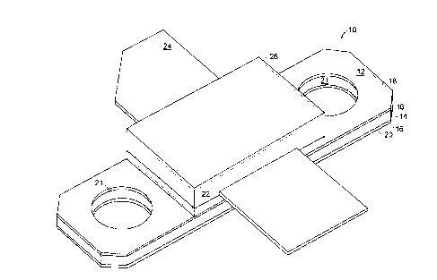
FIGURE 1 is an elevated perspective view of an electronic circuit device
package in accordance with one embodiment of the present invention in its sealed2 o condition.
FIGURE 2 shows the package of Fig. 1 with its cap removed to expose its
inner chamber.
FIGURE 3 is a sectioned view of the package of Figs. 1 and 2 without the
circuit device and connecting wires.
FIGURE 4 is an enlarged, sectional view of a portion of the section of Fig. 3
showing details of a brazed joint.
Detailed Description
In accordance with a preferred embodiment of the present invention, a
standard geometry circuit device package 10 as shown in Figs. 1-4 which is
identified in the industry by the designation RF701 and manufactured, for example,
CA 022S8438 l999-Ol-ll
DF3552
by the Brush Wellman Engineered Materials Company of Newburyport,
Massachusetts, is adapted to incorporate a CVD diamond film heat conducting
element. This package is especially suitable for housing RF (radio frequency)
devices which have a relatively high power output.
The main supporting structure of the package 10 is a metal laminate base
flange 12 which is adapted to be fastened to a heat sink member (not shown). Thebase flange 12 is a laminate which includes a core 14 of molybdenum about 24
mils thick bonded by a heat diffusion process directly to a copper cladding 16 about
8 mils thick over both its top face 18 and its bottom face 20. Bonded to the
10 copper of the top face 18 is an alumina frame 22 to which there are attached on
opposite top sides two copper power leads 24 which pass from the outside to the
inside of the package 10. A cap 26 hermetically seals the package 10.
The base flange 12 is a modified version of what is normally CuW (copper-
tungsten) base flange for this type of package. Normally, such a flange is entirely
15 of CuW. It is designed to have its bottom face 20 firmly fastened to the flatsurface of a heat sink member, such as a metal "slugl', by means of screws whichextend through two fastening holes 21. The present, modified version of the baseflange 12 is made as a laminate because the molybdenum core has a CTE which
closely matches that of the silicon circuit device to be housed in the package. The
20 copper cladding is provided to permit assembly of the package components in the
same manner as if the base flange 12 were copper-tungsten, thus eliminating the
need for developing specialized machinery and procedures for this process.
Fig. 2 shows the package of Fig. 1 with the cap 26 removed to reveal a
silicon circuit device 28 disposed in a chamber 29 formed by an opening 40
25 through the base flange 12. The device 28 is electrically connected to the two
copper power leads 24 by means of a plurality of bonding wires 28 and is attached
by a thermally-conductive bonding agent to a heat conducting floor member, or
substrate 32 made of diamond film about 350 micrometers thick~ The diamond
substrate 32 to which the device 28 is attached is metallized over its entire surface
30 with first a titanium layer about 1000 Angstroms thick, then a layer of platinum
about 2000 Angstroms thick, and then a layer of gold about 3.75 microns thick.
CA 022~8438 l999-Ol-ll
DF3552
The attachment is carried out by heating the package and pressing the device 28
against the metallizing 38 while vibrating it horizontally to form a gold-silicon
eutectic interface and is a known process. Such an interface provides an intimate
thermal and electrical contact. The bottom of the device 28 has a base electrical
lead which becomes connected to the base flange via the metallizing 38.
The Fig. 3 shows the package 10 in section, with the cap 26, device 28, and
bonding wires 30 removed. It is seen that the diamond substrate 32 is inlaid into a
shallow well 34 formed in the bottom surface of the base flange 12, so that it
abuts a shoulder 36. As is shown in greater detail in Fig. 4, the substrate 32 is
lO brazed to the shoulder 36 by means of a gold-indium braze 37 which is 81weight
% gold and 19 weight % indium and is sufficiently malleable to accommodate the
small degree of CTE mismatch between the diamond substrate 32 and the
molybdenum of the base flange 12. The well 34 is made just deep enough so that
the diamond substrate 32 fits into it to become flush with the bottom surface 20 of
15 the base flange 12. When the base flange is fastened to a heat sink member (not
shown), with an appropriate thermal interface compound, such as a thermal grease(e.g. a wax loaded with finely-divided thermal conductor, such as diamond or boron
nitride), the diamond substrate 32 makes optimum intimate contact with the heat
sink for maximizing heat transfer.
In practice, the thickness of the diamond is chosen to suit the needs of the
circuit in terms of how much heat spreading and how much total heat conduction
rate is required. The well 34 is then dimensioned to accommodate those
dimensions of the diamond substrate 32. The calculations for such design
parameters are known to those in the art.
General Considerations
While in the embodiment described above, the core of the base flange is
molybdenum and the substrate is diamond, the invention is applicable to other
choices of these materials and need not be a laminate at all. For example, the base
30 flange could be entirely of CuW, entirely of tungsten, or entirely of aluminum silicon
carbide. However, for base flange materials which present a greater CTE mismatch
, . .. .. .... . . ... . ..
CA 022S8438 l999-Ol-ll
DF3552
problem for the device being housed, it will be necessary to limit more severely the
temperature excursions of the device.
The attachment of the substrate to the shoulder of the base flange can be by
other bonding methods, depending upon their suitability otherwise for the particular
5 structure involved. The braze 37 used in the package 10 forms a particularly
intimate thermal contact between the members and has excellent mechanical
integrity. This leaves the substrate with not only a very high heat flux passingthrough its thickness to the outside, but also a very high heat flux passing to the
base flange member from its edges where they are brazed. In some applications,
0 the heat transfer from the edges may be less important. In that case other bonding
agents, such as solders or epoxies, may be sufficient. An alternative braze which
could be used in place of the gold-indium combination would be one of 20 weight
% copper and 80 weight % silver. In that case the metallizing would be replaced
by one which has a first layer of titanium about 1000 Angstroms thick, then a layer
15 of tungsten about 2000 Angstroms thick, then a layer of platinum about 2000
Angstroms thick, and finally a layer of nickel about 2 microns thick.
For situations in which removal of heat from the edges of the diamond
substrate is not considered important, the means of attaching the substrate to the
base flange is less important, and can be accomplished, for example, without any20 metallizing and by simply a suitable organic adhesive. Likewise, where the heat
removal from the device to the diamond substrate need not be maximized, there
may be used other means of fastening the device to the substrate which do not
require metallizing.
The details of the leads and how they are held in place on the package and
25 connected to the housed device are not considered a part of the invention and may
be a matter of choice. Likewise, the manner in which the housing is sealed is a
matter of choice. It is of key importance, however, that the device be directly
thermally coupled to one side of the diamond substrate and that the diamond
substrate be directly thermally coupled to a heat removal means. By "directly
30 thermally coupled" is meant that the only intervening material, if any, between
members so coupled is a thermal coupling agent which is viscously deformed by
CA 022~8438 1999-01-11
DF3552
pressure between the members and has a resulting thickness less than 10 microns.It does not include a structure in which a solid polyimide or other film of about 25
microns or more in thickness is interposed between the members. It does include
the use of a settable adhesive, solder, braze, or thermal grease.
If the package is housing a device which does not require attachment to a
conductive substrate for providing an electrical lead connection, then the diamond
substrate can have metallizing on its inside surface only where needed for brazing
and for attaching the device. On its outside surface, it then needs to have
metallizing only as required for providing a good thermal coupling to whatever
10 means are used for removing the heat conducted to that outside surface.
Rather than be inset into a shallow well, as is the case for the diamond
substrate 32 of the package 10, the diamond substate could also be simply be
attached to the bottom surface of the base flange, overlapping the edge of an
opening in the flange for forming a housing chamber, so long as this suits the needs
15 of the heat removal means for removing heat from the outside surface of the
diamond. For example, in such a case it may be necessary to provide spacers of
the same thickness as the diamond substrate under the holes for fastening the
package to a heat sink in order to prevent bending of the base flange as a result of
a cantilever effect from the diamond substrate being raised above the bottom
20 surface of the base flange.
The invention can be adapted to a wide variety of packages which feature a
base flange which is designed to act as a heat removal member for the housed
device. the adaptation involves removing at least that portion of the base flange
which would support the device and replacing it with diamond film substrate of a25 thickness which meets the demands of thermal management of the device. In
addition, the diamond film substrate should be located so that it properly couples
the output heat of the package to heat removal means. If the package is to be
mounted to a solid heat sink, it may be necessary to have the substrate flush with
the lower surface of the base flange to be mounted. If the heat removal is by fluid
30 flow or liquid spray, this may not be necessary.