Note : Les descriptions sont présentées dans la langue officielle dans laquelle elles ont été soumises.
CA 02262728 1999-02-23
1
OPTICAL DEMULTIPLEXER FILTER SYSTEM TO
ELIMINATE CROSS-TALK SIDE-LOBES
Field of the invention
s The invention relates to optical transmission systems, and
more particularly relates to so-called power divergence that
occurs within an optical transmission system.
Background of the Invention
The gain of an optical amplifier is typically not flat over the
o response of the amplifier -- which means that different levels of
gain are applied to optical signals of different wavelengths. FIG.
1 illustrates the response of a typical erbium doped optical
amplifier. Referring to the section designated R, a greater level
of amplification occurs for those signals having wavelengths
s from 1553 nm to 1559 nm than for those signals in the R region
and having wavelengths from 1548 nm to 1552 nm. Thus,
some optical signals are amplified greater. than other optical
signals passing through the optical amplifier. This difference in
amplification is referred to herein as power divergence, and
Zo needs to be dealt with.
Summary of the Invention
I have recognized that the severity of the power divergence
problem is directly proportional to the number of power amplifiers
disposed in an optical transmission path as well as the number
Zs of optical channels that are being transported over the path. I
have also recognized that when the channels are demultiplexed
CA 02262728 2001-10-24
2
at an intended destination some of the demultiplexed signals contain
appreciable levels of signals from the other channels, i.e., significant
levels of so-called cross-talk, as a result of such power divergence.
I deal with this problem by inserting, in accordance with an
aspect of the invention, loss in the path of each of the significantly
affected channels to greatly decrease the level of cross-talk in each of
those channels. In accordance with another aspect of the invention,
all of the significantly affected demultiplexed channels are passed
through a single loss device, which similarly decreases the level of
1o cross-talk in each of the significantly affected channels.
In accordance with one aspect of the present invention there is
provided an optical transmission system having first and second
optical nodes which communicate via an optical transmission path
such that the first optical node transmits an optical composite signal
formed from a plurality of optical signals of respective wavelengths to
the second optical node, in which the optical transmission path
contains a plurality of spaced-apart optical amplifiers, the optical
transmission system further comprising: demultiplexer means at the
second optical node for demultiplexing the composite optical signal
2o after it has been received by the second optical node into the plurality
of optical signals having respective wavelengths and for then coupling
the demultiplexed optical signals to respective output paths; and at
least one transmission filter device inserted in the respective output
path of at least one of the demultiplexed optical signals to suppress
the level of at least one other one of the demultiplexed optical signals
that may have been coupled to the respective output path as a result
CA 02262728 2001-10-24
2a
of optical-amplifier power divergence and to pass said one of the
demultipilexed signals to an output terminal.
In accordance with another aspect of the present invention
there is provided an optical system having an optical transmission
path and a plurality of spaced-apart optical amplifiers each operative
for amplifying an optical signal received via the transmission path, the
optical signal being formed from a plurality of optical signals of
respective wavelengths, the optical system further comprising: an
optical node connected to the transmission path and containing an
optical demultiplexer that demultiplexes the optical signal when it is
received at the optical node into the plurality of optical signals of
different wavelengths and couples the demultiplexed signals to
respective output paths, in which individual ones of the demultiplexed
signals include, as a result of power divergence caused by at least
one of the optical amplifiers, components of other ones of the
demultiplexed signals; and at least one transmission filter device
having a group of inputs coupled to respective ones of the output
paths such that the at least one transmission filter device passes the
signals respectively demultiplexed to the respective one of the output
2o paths and suppresses to a particular degree the levels of the included
component signals.
In accordance with yet another aspect of the present invention
there is provided an optical system for receiving a composite optical
signal via an optical transmission path having a plurality of spaced-
apart optical amplifiers disposed along the optical transmission path,
the composite optical signal being formed from a plurality of optical
signals of respective wavelengths, the optical system further
CA 02262728 2001-10-24
2b
comprising: a demultiplexer for demultiplexing the composite signal
into the plurality of optical signals after the composite signal has been
received via the optical transmission path and for then coupling the
demultiplexed optical signals to respective outputs, wherein at least
one of the demultiplexed optical signals includes, as a result of power
divergence caused by at least one of the optical amplifiers,
components of individual ones of the other ones of the optical signals
forming the composite signal; and at least one transmission filter
operative for passing the at least one demultiplexed optical signal to
to an output terminal and for suppressing the levels of the component
signals included with the at least one demultiplexed optical signal.
Brief Description of the Drawinas
FIG. 1 illustrates a typical response of an erbium doped optical
amplifier and is useful for understanding the underlying problem;
FIG. 2 shows a broad block diagram of an optical transmission
system arranged in accordance with the principles of the invention;
FIG. 3 illustrates different levels of power divergence that may
occur among optical channels;
CA 02262728 1999-02-23
3
FIG. 4 illustrates a number of different curves that are
useful in understanding and appreciating the principles of the
invention;
FIG. 5 illustrates the levels of cross-talk that occurs among
s the optical channels for different levels of power divergence;
FIG. 6 illustrates the effect of the principles of the
invention; and
FIG. 7 illustrates a portion of FIG. 1 arranged in
accordance with another embodiment of the invention.
o Detailed Description
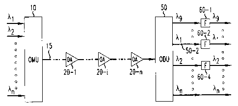
In an illustrative embodiment of the invention, FIG. 2, a
number, e.g., sixteen, of different optical signals having
respective wavelengths of ~,~, ~,2, ~,3 through ~,~ are supplied to a
conventional optical multiplexer (OMU) 10 in an optical node.
~s Multiplexer 10, which may be, for example, a so-called Dragone
router, multiplexes the optical signals ~,~ through ~,n in a
conventional manner to form a composite optical signal, and
then transmits the composite signal over transmission path 15.
For the following discussion, assume that the length of
Zo transmission path 15 is substantial, requiring amplification of the
optical signal at different points along the path. To meet that
requirement, assume that the path contains a number of spaced-
apart optical amplifiers 20-1 through 20-n, e.g., eight erbium
doped amplifiers.
Zs As discussed above, the amplification of certain optical
signals by each of the amplifiers 20-1 through 20-n will be
CA 02262728 1999-02-23
4
greater than the amplification of other ones of the optical signals,
causing a power divergence to be created between the signals.
I have recognized that the level of such power divergence is a
function of the number of active optical channels (bandwidths)
s and number of cascaded amplifiers that will amplify the
channels. Currently, the greatest number of optical channels
that is being used in an optical system is sixteen. However, that
number may soon increase to 75 or more channels, which will
exacerbate the power divergence problem. The power
o divergence problem is illustrated in FIG. 3 which shows power
divergence curves 21 and 22 respectively characterizing a power
divergence of 11 dB and 14 dB, that may occur in systems
having 16 active channels and approximately eight erbium
doped optical amplifiers in the transmission path. Curve 22
~s shows that a power divergence of approximately 14 dB occurs
between channels 7 and 9. Curve 21, on the other hand, shows
that a power divergence of 11 dB occurs between those two
channels. (Note that in an optical transmission path, power
divergencies of 11 dB and 14 dB may occur at the output of the
Zo seventh and eighth optical amplifiers.) A large power divergence
also occurs between channel 9 and other channels , e.g.,
channels 5, 14, 15, 16 and 8. This is true for still other channels,
namely, channels 1, 2 and 10, as is shown by FIG. 3 -- which
means that it is likely that when channel 9, 1, 2 and 10 are
Zs demultiplexed in a conventional way at a destination node, then
those demultiplexed signals will contain cross-talk from the
CA 02262728 2001-10-24
channels having stronger signals. This problem is illustrated in FIG. 4
showing the signal spectrum for demultiplexed channel 1 (wavelength
of 1549.315 nm) at the output of ODU 50 (e.g., a so-called Dragone~
router) in an optical node. It is seen from the spectrum shown in FIG.
5 4 that demultiplexed channel 1 also contains, as a result of the power
divergence between channel 1 and the other aforementioned
channels, significant levels of "cross-talk" or signal components from
other channels (as shown by curve section 31 ). Curve 32 shows a
more ideal case in which the such cross-talk is suppressed, in
1o accordance with an aspect of the invention, as will be discussed
below.
From a system design perspective, total cross-talk should be
limited to 13 dB, as shown in FIG. 5 illustrating four different curves
for different levels of power divergence for an optical system having a
number of, e.g., eight, cascaded optical amplifiers in the transmission
path as shown in FIG. 2. Note that a power divergence of 5 dB, 8 dB,
11 dB and 14 dB typically occurs at the output of the fourth or fifth
amplifier, seventh amplifier and eighth amplifier, respectively. It is
seen from FIG. 5 that for a power divergence of, e.g., 14 dB
(identified by the + points), channels 9, 1, 10 and 2 do not meet a
predetermined cross-talk limit, e.g., a limit of 13 dB. (Note, for
example, that for most other cases, channels 9, 1 and 10 still do not
meet the 13 dB cross-talk limit, see, for example the curve for a
power divergence of 8 dB (designated by the D points)).
CA 02262728 1999-02-23
6
I have recognized that for the optical system of FIG. 2 and
for optical systems having a large number of optical amplifiers in
the transmission path or span, the level of cross-talk contained
in a demultiplexed signal as a result of the power divergence
s problem may be dealt with by suppressing the cross-talk. This
may be done, in accordance with an aspect of invention, by
adding additional loss to a demultiplexed signal in a way that
suppresses the cross-talk only. More specifically, by inserting a
"loss device" in the path of a demultiplexed signal such that the
device suppresses only the cross-talk that may be present in the
demultiplexed signal. In accord with another aspect of the
invention, I achieve this result by placing a thin-film filter at the
port of the demultiplexer which couples to an output a
demultiplexed signal containing a level of cross-talk which does
~s not meet the predetermined limit, e.g., 13 dB. The thin-film filter,
which is tuned to the demultiplexed signal, allows the
demultiplexed signal to easily pass through the filter, but
suppresses other optical signals, especially the optical signals
that are due to cross-talk, as is represented by curve 32, FIG. 4.
20 (Each such thin-film may be obtained from Oplink
Communications Inc. of Hoboken, New Jersey, USA as Part No.
IBPF-5LT-16-1-1. Note that curve 33 characterizes the loss
response of the thin-film filter, which greatly suppresses the
signals in section 31 of response curve 34, as is illustrated by
as curve section 32. In accordance with a particular embodiment of
the invention explained below, the thin-film filter is tuned to
CA 02262728 1999-02-23
7
channels 9, 1, 10 and 2 and may be disposed such that the
demultiplexed signals corresponding to those channels are
coupled to respective input ports of the thin-film filter. The
coupled optical signals then pass through the filter such that the
s filter suppresses only the cross-talk in each of those signals.
(Note that the latter filter may also be obtained from Oplink
Communications Inc. of Hoboken, New Jersey, USA as Part
Number IBPF-5LT-16-1-1.) Thus, a single thin-film filter may be
used to filter four optical signals instead of four individually tuned
filters, which greatly reduces the cost of adding loss to the
demultiplexed signals to suppress cross-talk.
The effect of this aspect of the invention is shown in FIG.
6. Specifically, curve 41 is the loss response of the thin-film filter
covering channels 9,1,10 and 2, as represented by curve 42. It
~s is seen from the FIG. that the loss response represented by
section 41A of the filter response greatly suppresses the cross-
talk, designated as section 42A of curve 42.~.
Returning to FIG. 2, the composite signal is amplified by
each of the optical amplifiers (OA) 20-1 through 20-n and the
ao final amplified result is supplied to optical demultiplexing unit
(ODU) 50, which also may be, e.g., a Dragone router. ODU 50
demultiplexes the composite signal into constituent signals of
respective wavelengths 7~~ through ~,~, in which the first four
signals, corresponding to channels 9, 1, 10 and 2, contain cross-
Zs talk signals the level of which do not meet the 13 dB
requirement, as represented in the FIG. by the superscript *. To
CA 02262728 1999-02-23
8
address that problem a thin-film filter (F) having the appropriate
loss response, e.g., the response shown in FIG. 3 as curve 33, is
inserted into the output path of a significantly affected signal.
For example, a thin-film filter (F) 60-2 having the response
s shown in FIG. 4 is inserted in the output path 50-2 to suppress
the cross-talk contained in channel 1, such that the response of
the signal at the output of filter 60-2 is characterized by curve 32
of FIG. 4. Appropriate thin-film filters 60-1, 60-3 (not shown) and
60-4 are also inserted in the output paths of the other
significantly affected signals, namely channels 9, 10 and 2.
It is noted that such an appropriate filter may be
respectively inserted in the output paths of the other channels to
suppress the cross-talk contained in those channels, if it is so
desired.
~s FIG. 7 is a partial block diagram of FIG. 2 modified to show
the embodiment of the invention in which one thin-film filter 70-1
is used to suppress the cross-talk in channels 9, 1, 10 and 2.
FIG. 7 also shows that another thin-film filter, e.g., filter 70-2,
may be used to suppress the cross-talk present in another group
ao of channels, in which the response of filter 70-2 covers the
response for that group of channels similar to the manner shown
in FIG. 6.
The foregoing is merely illustrative of the principles of the
invention. Those skilled in the art will be able to devise
Zs numerous arrangements, which, although not explicitly shown or
CA 02262728 1999-02-23
described herein, nevertheless embody those principles that are
within the spirit and scope of the invention.