Note : Les descriptions sont présentées dans la langue officielle dans laquelle elles ont été soumises.
CA 02277644 1999-07-14
TRIPHENYLAMINE DERIVATIVE AND ORGANIC
ELECTROLUMINESCENCE DEVICE COMPRISING THE SAME
FIELD OF THE INVENTION
The present invention relates to a novel
triphenylamine derivative which can be preferably used as a
hole-transporting material, e.g., for organic
electroluminescence device and an organic
electroluminescence device comprising the same.
BACKGROUND OF THE INVENTION
As an organic electroluminescence device comprising
an organic layer mainly comprising an organic compound
provided interposed between a pair of electrodes, i.e.,
cathode and anode there had been generally used one
comprising a single organic layer. In recent years,
however, various organic electroluminescence devices
comprising a plurality of organic layers each independently
having a function such as emission of light and
transportation of carrier (e.g., hole, electron) (as
disclosed in C. W. Tang and S. R. VanSlyke, "Appl. Phys.
Lett.", 51, 913 (1987), C. Adachi, T. Tsutsui and S. Saito,
"Appl. Phys. Lett.", 55, 1489 (1989), J. Kido, M. Kimura,
and K. Nagai, "Science", Vol. 267, 1332 (1995) ).
Such an organic electroluminescence device has the
following advantages:
1
CA 02277644 1999-07-14
(1) It can emit light with a high luminance at a low
voltage as compared with the conventional devices mainly
comprising inorganic material;
(2) Since the formation of the various layers can be
accomplished not only by vacuum evaporation method but also
by solution coating method and any method can be selected
taking into account the structure of each of the various
layers, the degree of freedom of device design is enhanced,
making it possible to enlarge the surface of device; and
(3) A multi-color system can be provided by designing
the organic molecules.
Examples of the various layers constituting the
organic layer comprising a plurality of layers include
light-emitting layer, hole-transporting layer capable of
transporting hole, and electron-transporting layer capable
of electron. These layers are each formed by the foregoing
organic compounds having excellent various properties or by
dispersing those organic compounds in an appropriate
polymer binder.
However, the conventional organic electroluminescence
devices are disadvantageous in that they exhibit
insufficient stability and durability mainly attributed to
(1) deterioration of organic compound itself due to Joule's
heat developed when the device is energized or (2)
deterioration in the carrier injection efficiency between
various layers due to the reduction in smoothness of
interface caused by the crystallization of organic compound
2
CA 02277644 1999-07-14
by Joule's heat thus developed, and hence exhibit a
drastically reduced luminance during a repeated use.
The foregoing problem is remarkable particularly with
a hole-transporting material having a low heat resistance
constituting a hole-transporting layer among the organic
compounds constituting the foregoing various layers. It is
not too much to say that the heat resistance of organic
electroluminescence devices is determined by the heat
resistance of such a hole-transporting material.
Under these circumstances, extensive studies have
recently been made on the molecular structure of such a
hole-transporting material to improve the heat resistance
thereof.
For example, Adachi et al. attempted to improve the
heat resistance by polymerizing a triphenylamine derivative
known as a hole-transporting material such as N,N'-
diphenyl-N,N'-bis(3-methylphenyl)-1,1'-biphenyl-4,4'-
diamine (hereinafter abbreviated as "TPD", which represents
a dimer of triphenylamine) represented by the following
formula ( 3-1 ) .
/ \ / \
t3--_~
CH3 ~''3C
3
CA 02277644 1999-07-14
As a result, it was reported that a triphenylamine trimer
(hereinafter referred to as "HTM1") represented by the
following formula (4):
CH3
/I
N
w I ~ I / CH3 (4)
H3~ / / ~ I ~ i
N ~ I N
/ I
w
CH3 CH3
exhibits a high heat resistance and an excellent hole-
transporting capacity (C. Adachi, K. Nagai and N. Tamoto,
~Appl. Phys. Lett.", 66 (20), 2679 (1995)).
Further, Tokito et al. also attempted to improve the
heat resistance by polymerizing a triphenylamine derivative
in a similar manner as described above.
As a result, it was clarified that a triphenylamine
tetramer (hereinafter referred to as ~TPTE") represented by
the following formula (5-1):
4
CA 02277644 1999-07-14
(5-1)
C ~ ~ H3
CH3
exhibits a high heat resistance and an excellent hole-
transporting capacity (S. Tokito, H. Tanaka, A. Okada and Y.
Taga, "'Appl. Phys. Lett.", 69(7), 878 (1996); S. Tokito, H.
Tanaka, K. Noda, A. Okada and Y. Taga, ~Macromol. Symp.",
125, 181-188 (1997); JP-A-10-25473 (The term "JP-A" as used
herein means an "unexamined published Japanese patent
application")).
Further, JP-A-7-126226 discloses that a benzidine
compound obtained by normalizing the biphenyl ring in the
center of the foregoing TPTE into various divalent groups
containing the biphenyl ring and normalizing the kind of
substituents on various rings and the substitution
positions thereor exhibits an excellent stability at the
time of light emission and storage, as compared with low
molecular weight hole-transporting materials such as the
foregoing TPD.
The inventors made studies on the foregoing problems.
It was found that the foregoing various polymerized
/ \
N
CA 02277644 1999-07-14
compounds or their peripheral compounds certainly exhibit a
stabilized heat resistance and stability as compared with
the conventional TPD but leave something to be desired in
their effects. In particular, these compounds cannot
satisfy the high heat resistance required for on vehicle
display devices.
In other words, on vehicle display devices must
operate without any trouble even when continuously driven
at a temperature as high as 85°C and a humidity as high as
85~RH for 240 hours. Thus, the on vehicle display device,
if it is in the form of organic electroluminescence device,
must not show a drastic drop of luminance or stop light
emission even when continuously operated under the
foregoing high temperature and humidity conditions for 240
hours.
However, HTM1 (a trimer of triphenylamine)
represented by the foregoing formula (4) exhibits a glass
transition temperature Tg of about 110°C and hence shows a
difference as small as 25°C from the foregoing ambient
temperature, demonstrating that it exhibits an insufficient
heat resistance. Thus, if continuously operated at such a
high temperature and humidity, the foregoing generation of
Joule's heat causes the temperature of the device itself to
exceed the glass transition temperature Tg of HTM1 in an
extremely short period of time, resulting in deterioration
of the foregoing organic compound itself, i.e., HTM1 itself,
or reduction in the injection efficiency between layers.
6
CA 02277644 1999-07-14
Further, the thickness of the organic layer
constituting the device is as extremely small as about 0.1
um in total, even if the organic layer comprises a
plurality of layers. Thus, if there is some dispersion of
thickness, current is concentrated into the section having
the smallest thickness to cause local rise in temperature,
resulting in the cracking and peeling of the organic layers
that cause short-circuiting between the cathode and the
anode.
It is thus expected that a device comprising HTM1
shows a drastic drop in luminance or stops light emission
in a short period of time due to the foregoing defects.
The insufficient heat resistance of the organic
electroluminescence device using HTM1 is also apparent from
the fact described in the report by Tokito et al. that a
device comprising TPTR, which is different from HTM1 only
in the substitution position of terminal methyl group, has
a critical temperature as described below of about 110°C.
This is also applicable to TPTE represented by the
foregoing formula (5-1). In other words, TPTE exhibits a
glass transition temperature Tg of 130°C and hence shows a
temperature difference as small as 45°C from the foregoing
ambient temperature of 85°C. Thus, if continuously
operated at such a high temperature and humidity, it can be
expected that the resulting deterioration of TPTE itself or
the injection efficiency between layers or the short-
circuiting between the cathode and the anode causes the
7
CA 02277644 1999-07-14
device to show a drastic drop of luminance or to stop light
emission in a short period of time.
The above described reference discloses that the
upper limit of temperature at which an organic
electroluminescence device comprising TPTE can operate is
140°C. However, this temperature merely indicates the
temperature (critical temperature) at which light emission
stops when the ambient temperature is gradually raised
while the device is being allowed to emit light. Thus, the
temperature at which the device can stably and continuously
emit light over an extended period of time was not
confirmed therein.
According to the inventors' study, the organic
electroluminescence device comprising TPTE is
disadvantageous in that it exhibits too small an external
quantum efficiency to emit light with a high luminance at a
small current.
This phenomenon is considered to be attributed to the
fact that TPTE forms, for example in a multi-layer
structure device, an exciplex with an electron-transporting
material such as tris(8-quinolilato) aluminum (III) complex
(hereinafter referred to as "Alq") represented by the
following formula (6):
8
CA 02277644 1999-07-14
/ \
N
,
,
__Ai,-p ,
,,
I O~ ,,, I
I N
contained in the adjacent electron-transporting layer due
to the interaction at the interface of the layers.
In an attempt to enhance the external quantum
efficiency of devices by preventing the formation of such
an exciplex, Noda et al. made a study on the molecular
structure of TPTE. As a result, it was clarified that the
foregoing object can be accomplished by employing a meta-
position-linkage structure represented by the following
formula (5-2):
I ~ I
i ( i I N \ I ~ I N (5-2)
N ~ ~ I ~ I ~,N ~ / I ~ I
~I ~I
(Koji Noda, Hisayoshi Fujikawa, Katsunori Koda, Hisato
Takeuchi, Seiji Tokito, Yasukuni Taga, "Preprint of 45th
Joint Forum of Society of Applied Physics", Tokyo
Engineering University, March 1998).
However, the foregoing meta-position-linkage TPTE
(hereinafter referred to as '~m-TPTE") is disadvantageous in
9
CA 02277644 1999-07-14
that it exhibits a glass transition temperature as low as
about 90°C and thus cannot be used for the purpose
requiring a high heat resistance and reliability as in the
foregoing on vehicle display device.
An object of the present invention is to provide a
novel triphenylamine derivative which has further excellent
heat resistance as compared to the conventional compounds
and which is not accompanied with concern about easy
formation of an exciplex with an electron-transporting
material.
Another object of the present invention is to provide
an organic electroluminescence device which comprises the
triphenylamine derivative and thus has a high heat
resistance and a high luminous efficiency at the same time.
Other objects and effects of the invention will
become apparent from the following description.
To solve the foregoing problems, the inventors made
extensive studies on the structure of triphenylamine
derivative.
As a result, it was found that a compound obtained by
replacing each one of the respective two phenyl groups
connected to a nitrogen atom (N) at both terminals of the
foregoing TPTE, i.e., two phenyl groups in total, by a
naphthyl ring or higher aromatic condensed ring as shown in
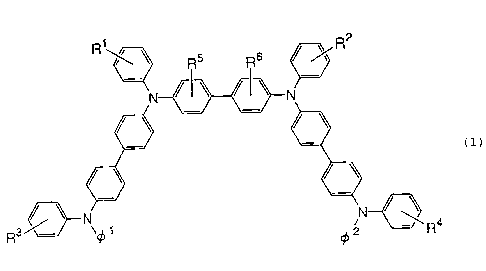
the following general formula (1):
CA 02277644 1999-07-14
2
R5 R6
(1)
~\ Ra
R3~~ ~~ 1 ~ 2
wherein Rl, R2, R3, R4, R' and R6 may be the same or
different and each represents a hydrogen atom, alkyl group,
halogenated alkyl group, aryl group, dialkylamino group or
cyano group; and ~1 and ~' may be the same or different and
each represents an aromatic condensed ring which may have a
substituent, has the following advantages:
(1) The compound has a glass transition temperature
Tg of not lower than about 140°C and hence has a
drastically improved heat resistance while maintaining the
high hole-transporting capacity inherent to TPTE; and
(2) The compound hardly forms an exciplex assumingly
because of its stereostructure having substituted large
aromatic condensed rings at its terminals or because of the
distribution of ~ electron conjugated system.
The present invention has thus been worked out.
That is, the foregoing objects of the present
invention have achieved by providing the following
triphenylamine derivative and organic electroluminescence
devices.
11
CA 02277644 1999-07-14
1) A triphenylamine derivative represented by the
following general formula (1):
r,2
(1)
Ra
/.
wherein R1, R-, R3, R4, RS and R6 may be the same or
different and each represents a hydrogen atom, alkyl group,
halogenated alkyl group, aryl group, dialkylamino group or
cyano group; and ~1 and 4~ may be the same or different and
each represents an aromatic condensed ring which may have a
substituent.
2) An organic electroluminescence device comprising a
cathode, an anode and an organic layer interposed between
said electrodes, wherein said organic layer contains as a
hole-transporting material a triphenylamine derivative
represented by the following general formula (1):
12
CA 02277644 1999-07-14
n2
(1)
Ra
Rs~ y i
wherein R', RZ, R', R4, RS and RG may be the same or
different and each represents a hydrogen atom, alkyl group,
halogenated alkyl group, aryl group, dialkylamino group or
cyano group; and ~i and ~2 may be the same or different and
each represents an aromatic condensed ring which may have a
substituent.
3) The organic electroluminescence device according
to the above 2), wherein said organic layer comprises a
single organic layer or a plurality of organic layers and
at least one of said organic layers contains a
triphenylamine derivative represented by general formula
(1) .
9) The organic electroluminescence device according
to the above 3),
wherein said anode is an electrically-conductive
transparent layer which comprises an electrically-
conductive transparent material and which is formed on a
substrate, and
13
CA 02277644 1999-07-14
wherein said layer containing the triphenylamine
derivative is a hole-transporting layer provided on said
electrically-conductive transparent layer directly or via a
single hole-injecting layer.
5) The organic electroluminescence device according
to the above 3), wherein said layer containing the
triphenylamine derivative further contains at least one
fluorescent dye.
6) The organic electroluminescence device according
to the above 3), said organic layer comprises a layer
containing as an electron-transporting material a 1,2,4-
triazole derivative represented by the following general
formula (2):
~ N
w ~N n N
(2)
R~ / / ~ ~ Ra
wherein R' and RE may be the same or different and each
represents a cyano group or diarylamino group; and n
represents an integer of 1 or 2.
7) The organic electroluminescence device according
to the above 2), wherein said triphenylamine derivative is
represented by the following formula (1-3):
14
CA 02277644 1999-07-14
~ CN3 H3C
( 1-3 ) .
Japanese Patent 2,851,185 discloses a device
comprising a positive hole-transporting aromatic tertiary
amine containing at least two tertiary amine components and
at least two condensed aromatic rings connected to the
nitrogen atom in the tertiary amine.
However, a further review of specific examples of the
positive hole-transporting aromatic tertiary amine
described in the 32nd column of the above cited patent
shows that the tertiary amine thus proposed is nothing but
one obtained by replacing at least two of phenyl groups or
the like in a low molecular weight hole-transporting
material having a unpolymerized base structure such as the
foregoing TPD by condensed aromatic rings.
Further, the effect of the tertiary amine thus
proposed is nothing but to improve the stability of the
device as compared with the low molecular weight hole-
transporting material. The above cited patent does not
disclose or suggest improving the heat resistance of
CA 02277644 1999-07-14
devices at high temperatures conditions together with
improving the luminous efficiency thereof as attained in
the present invention.
On the other hand, the present invention has been
worked out on the basis of a new knowledge that by
polymerizing the triphenylamine derivative to increase the
resulting glass transition temperature Tg, the device has
an unprecedentedly enhanced heat resistance at high
temperatures and the formation of an exciplex accompanying
the polymerization can be avoided on account of the
condensed aromatic rings introduced into the molecule, to
thereby enhance the luminous efficiency of the device.
Accordingly, the present invention is not a mere
combination of the foregoing polymerization technique
developed by Tokito et al. and the condensed aromatic ring
described in the above cited patent.
BRIEF DESCRIPTION OF THE DRAWINGS
Fig. 1 is a graph illustrating 1H-NMR chart of NPTE-1
of the present invention synthesized in Synthesis Example 1.
Fig. 2 is a graph illustrating IR chart of NPTE-1.
Fig. 3 is a graph illustrating DSC chart of NPTE-1.
Fig. 4 is a graph illustrating IR chart of NPTE-3 of
the present invention synthesized in Synthesis Example 2.
Fig. 5 is a graph illustrating the voltage-luminance
characteristics of the organic electroluminescence device
prepared in Example 1.
16
CA 02277644 1999-07-14
Fig. 6 is a graph illustrating the emission spectrum
of the device of Example 1.
Fig. 7 is a graph illustrating the luminance-external
quantum efficiency characteristics of the device of Example
1:
Fig. 8 is a graph illustrating the temperature-
luminance half-life characteristics of the organic
electroluminescence device prepared in Example 2 and
Comparative Example 1.
Fig. 9 is a graph illustrating the temperature-
external quantum efficiency characteristics of the device
of Example 2.
Fig. 10 is a graph illustrating the temperature-
external quantum efficiency characteristics of the organic
electroluminescence device prepared in Comparative Example
2.
Fig. 11 is a graph illustrating the temperature-
external quantum efficiency characteristics of the organic
electroluminescence device prepared in Comparative Example
3.
Fig. 12 is a graph illustrating the temperature-
external quantum efficiency characteristics of the organic
electroluminescence device prepared in Comparative Example
4.
nFTATT,F'D DESCRIPTION OF THE INVENTION
The present invention is described in detail below.
17
CA 02277644 1999-07-14
First, the triphenylamine derivative according to the
present invention is described in detail below.
As the alkyl group corresponding to R1, RZ, R', R4, RS
or R'' in the foregoing general formula (1) representing the
triphenylamine derivative of the present invention there
may be preferably used a C1_t, alkyl group such as methyl,
ethyl, n-propyl, isopropyl, n-butyl, isobutyl, sec-butyl,
tert-butyl, pentyl and hexyl.
As the halogenated alkyl group there may be used,
e.g., a group obtained by replacing all or some of hydrogen
atoms in the foregoing C1_d alkyl group by fluorine,
chlorine, bromine or iodine. Specific examples of such a
halogenated alkyl group include trifluoromethyl group (-
CF_), but the present invention should not be construed as
being limited thereto.
Examples of the foregoing aryl group include phenyl,
biphenyl, o-terphenyl, naphthyl, anthryl, and phenanthryl.
These aryl groups may have substituents such as the
foregoing alkyl group at arbitrary positions on the ring.
Specific examples of the aryl group having substituents
include tolyl, and xylyl, but the present invention should
not be construed as being limited thereto.
As the dialkylamino group there may be used a group
obtained by replacing both the two hydrogen atoms in the
amino group by the foregoing alkyl group. Specific
examples of such a dialkylamino group include diethylamino
group, but the present invention should not be construed as
being limited thereto.
18
CA 02277644 1999-07-14
Examples of the aromatic condensed ring corresponding
to ~1 or ~2 in the foregoing general formula (1) include
naphthyl, anthryl, and phenanthryl. Such an aromatic
condensed ring may have substituents such as. the foregoing
alkyl group at arbitrary positions on the ring.
Specific examples of the triphenylamine derivative of
the present invention represented by the general formula
(1) (hereinafter referred to as "triphenylamine derivative
(1)") include N,N'-diphenyl-N,N'-bis(N-phenyl-N-(2-
naphthyl)-4'-aminobiphenyl-4-il)-1,1'-biphenyl-4,4'-diamine
(glass transition temperature Tg: 148°C; hereinafter
referred to as "NPTE-1") represented by the following
formula (1-1):
/ \ / \
\ / \
/ \ / \
(1-1),
/ \ / \
/ \ N N / \
\ / \ / \
N, N' -bis ( 4- (tert-butyl ) phenyl ) -N, N' -bis (N-4- (tert-butyl)
phenyl-N-(2-naphthyl)-4"-aminobiphenyl-4-il)-l, l'-biphenyl-
4,4'-diamine (glass transition temperature Tg: 175°C,
hereinafter referred to as "NPTE-2") represented by the
following formula (1-2):
19
CA 02277644 1999-07-14
(1-2),
(HsC)s ~C(CH3)3
N,N'-diphenyl-N,N'-bis(N-phenyl-N-(2-naphthyl)-4'-amino
bipheny-1-4-il)-1,1'-biphenyl-3,3'-dimethyl-4,4'-diamine
(glass transition temperature Tg: 145°C, hereinafter
referred to as '~NPTE-3") represented by the following
formula (1-3):
N ~ ~ ~ ~ N
(1-3),
However, the present invention is not limited thereto.
The synthesis of the triphenylamine derivative of the
present invention can be accomplished, e.g., by the
following method. In the following description, synthesis
method is described with reference to the synthesis of
CA 02277644 1999-07-14
NPTE-1 represented by the foregoing formula (1-1) among the
triphenylamine derivatives of the present invention. In
practice, however, other triphenylamine derivatives (1) can
be synthesized similarly in principle.
N-phenyl-N-(2-naphthyl)amine represented by formula
(la) below and 4,4'-diodobiphenyl represented by formula
(lb) below as starting materials are reacted at a molar
ratio of 1 . 1 to synthesize 4-(N-phenyl-N-(2-
naphthyl))amino-4'-iodobiphenyl represented by the
following formula (lc).
~ NH
+ I
(1 a) (1 b)
N ~ ~
a
(1 c)
Thereafter, 4-(4-phenyl-N-(2-naphthyl))amino-4'-iodo
biphenyl represented by the foregoing formula (lc) is
reacted with N,N'-diphenylbezidine represented by formula
(ld) below at such a molar ratio that the former is more
excess than the case of a molar ratio of 2:1 to synthesize
NPTE-1 represented by the following formula (1-1).
21
CA 02277644 1999-07-14
/ \
r
2
1c
/ \ / \
HN ~ ~ ~-~ NH
(1 d)
/ \ / \
N / \ / \ N
/ \ / \
/ \
\ / ~N / \
/ \
(1-1>
22
CA 02277644 1999-07-14
The triphenylamine derivative of the present
invention as described above can be used as a photoreceptor
for an apparatus utilizing an electrophotographic process
such as copying machines or a hole-transporting material in
various fields such as solar batteries. In particular, the
triphenylamine derivative of the present invention is
preferably used as a hole-transporting material for organic
electroluminescence device as described above.
In particular, NPTE-3 represented by the foregoing
formula (1-3) can exert an excellent effect of enhancing
the luminous efficiency of organic electroluminescence
device in addition to the high heat resistance inherent to
the triphenylamine derivative (1) of the present invention
as made obvious from the results of examples described
below. Thus, NPTE-3 can be preferably used as a hole-
transporting material in particula r.
The organic electroluminescence device of the present
invention is described in detail below.
The organic electroluminescence device of the present
invention is not limited in its structure so far as at
least one of organic layers provided interposed between the
cathode and the anode contains the foregoing triphenylamine
derivative (1) of the present invention as a hole-
transporting material.
The organic layer may have either a single-layer or
multi-layer structure. Among these layer structures, the
organic layer having a single-layer structure may be formed
by the foregoing triphenylamine derivative (1) of the
23
CA 02277644 1999-07-14
present invention as a hole-transporting material alone
because the triphenylamine derivative has a high heat
resistance. Alternatively, the single-layer structure
organic layer may be formed by optionally adding other
hole-transporting materials or electron-transporting
materials, fluorescent dyes, etc. described below, in
addition to triphenylamine derivative (1) as needed.
Further alternatively, the foregoing various materials may
be dispersed in a polymer having or free of carrier-
transporting capacity itself as a binder to form a single-
layer organic layer.
The thickness of the single organic layer is about
the same as conventional, i.e., preferably from 50 to 1,,000
nm, particularly from 100 to 200 nm.
On the other hand, the number of layers and layer
constitution of the multi-layer organic layer are not
specifically limited. For example, the multi-layer organic
layer can be formed by properly selecting and combining two
or more of the following various layers sequentially from
the anode side to the cathode side. At least one of these
layers comprises triphenylamine derivative (1) of the
present invention incorporated therein as a hole-
transporting material.
(a) A layer which helps the injection of holes from
the anode to the cathode (hole-injecting layer);
(b) A layer which transports holes injected from the
anode to the cathode (hole-transporting layer);
29
CA 02277644 1999-07-14
(c) A layer which transports electrons injected from
the cathode to the anode (electron-transporting layer); and
(d) A layer which helps the injection of electron
from the cathode to the anode (electron-injecting layer)
These various layers may be each formed by only an
organic compound having a specific function. Alternatively,
these various layers may be each formed by dispersing the
foregoing organic compound in a polymer having or free of
carrier-transporting capacity itself as a binder.
Specific examples of the multi-layer organic layer
comprising the foregoing various layers include (A) a layer
structure comprising two layers, i.e., a hole-transporting
layer and an electron-transporting layer, either or both of
which is capable of emitting light, (B) a layer structure
comprising three layers, i.e., a hole-injecting layer, a
hole-transporting layer and an electron-transporting layer,
of which the hole-transporting layer and/or the electron-
transporting layer is capable of emitting light, (C) a
layer structure comprising three layers, i.e., a hole-
transporting layer, an electron-transporting layer and an
electron-injecting layer, of which the hole-transporting
layer and/or the electron-transporting layer is capable of
emitting light, and (D) a layer structure comprising four
layers, i.e., a hole-injecting layer, a hole-transporting
layer, an electron-transporting layer and an electron-
injecting layer, of which the hole-transporting layer
and/or the electron-transporting layer is capable of
CA 02277644 1999-07-14
emitting light, but the present invention should not be
construed as being limited thereto.
Which or both of the hole-transporting layer and the
electron-transporting layer emits light in the device
having the foregoing layer structure can be properly
predetermined by adjusting the degree and combination of
the functions of organic compounds contained in the two
layers (e. g., hole-transporting capacity if it is a hole-
transporting material or electron-transporting capacity if
it is an electron-transporting layer) , the thickness of the
various layers, etc.
Among the foregoing various layers, the layer capable
of emitting light may comprise one or more fluorescent dyes
incorporated therein to adjust the wavelength of light
emitted therefrom.
The triphenylamine derivative (1) of the present
invention may be incorporated in any of the foregoing
various layers but preferably in the hole-injecting layer
or hole-transporting layer.
Examples of organic compound having excellent hole-
injecting properties constituting the hole-injecting layer
among the foregoing various layers include a copper
phthalocyanine represented by the following formula (7):
26
CA 02277644 1999-07-14
N ~N ~ N
I 'N___Cu___N I
~ ; j ~ (~) ,
N~~N N
polyaniline, polythiophene, and carbon. The hole-injecting
layer may comprise a triphenylamine derivative (1) of the
present invention incorporated therein as mentioned above
in addition to the foregoing hole-injecting materials.
Alternatively, the hole-injecting layer may comprise hole-
transporting materials other than triphenylamine derivative
(1) incorporated therein.
As the hole-transporting material constituting the
hole-transporting layer there may be mainly used the
triphenylamine derivative (1) of the present invention.
Besides the triphenylamine derivative (1) of the present
invention, other known conventional hole-transporting
materials such as the foregoing TPD, TPTE, HTM1 and m-TPTE
and N,N'-diphenyl-N,N'-di(2-naphthyl)-1,1'-biphenyl-4,4'-
diamine (hereinafter referred to as "NPD") represented by
the following formula (3-2):
27
CA 02277644 1999-07-14
/ \ / \
cs-zl
may also be used in combination so far as the heat
resistance of the device is not impaired.
Examples of the electron-transporting material
constituting the electron-transporting layer include,
besides the above-described Alq, a 1,2,4-triazole
derivative (hereinafter referred to as ~DPTAZ2")
represented by the following formula (2-1):
I I
I I / / ~ w N ~ (2-i) .
,~ ~ I
I
I.
The electron-injecting layer comprises a material
having excellent electron-injecting properties among
electron-transporting materials. Examples of such an
electron-injecting material having excellent electron-
injecting properties include the foregoing Alq, and a
1,2,4-triazole derivative such as cyano group-substituted
28
CA 02277644 1999-07-14
triazole dimer (hereinafter referred to as "CNTAZ2")
represented by the following formula (2-2).
~N N / I
(2-2)
N ~ ~ ~ ~ ~ ~. CN
As the fluorescent dyes which may be incorporated in
the layer capable of emitting light among the hole-
transporting layer and/or electron-transporting layer there
may be used various dyes which can be excited by exciton
such as a dye for laser singly or in combination depending
on the desired wavelength of light emitted.
Specific examples of the fluorescent dye include
cyanine dye, xanthene dye, oxazine dye, coumarine dye,
quinacridone derivative, naphthacene derivative, perylene
derivative, acridine dye, acridone dye, and quinoline dye.
Specific examples of these fluorescent dye employable
herein include coumarine 6 (emitting green light)
represented by the following formula (8):
~N
(8).
H~C2.N ~ O O
C2H5
coumarine 7 represented by the following formula (9):
29
CA 02277644 1999-07-14
HN
~ ~N
N 0 (9),
C2Hs
quinacridone dyes (emitting green light) represented by the
following formulae (10-1) and (10-2):
- i ~7
(10-1)
(10-2)
wherein R1-, R1', Rig and R15 may be the same or different and
each represents a hydrogen atom, alkyl group or aryl group,
and rubrene (5,6,11,12-tetraphenylnaphthacene, emitting
yellow light) represented by the following formula (11):
H5C6 C6H5
(11) .
HsCs CsHs
Besides these fluorescent dyes, tetraphenyl butadiene,
dicyanomethylenestyryl pyrane-based dyes such as 4-
CA 02277644 1999-07-14
dicyanomethylene-2-methyl-6-p-dimethylaminostyryl-4H-pyrane,
perylene, Nile red, etc. may be used as fluorescent dyes.
The thickness of the foregoing various layers
constituting the multi-layer organic layer is not
specifically limited. In practice, however, these layers
each preferably have a thickness of from 5 to 100 nm,
particularly from 10 to 80 nm.
The total thickness of the multi-layer organic layer
obtained by laminating two or more of the foregoing layers
is preferably from 80 to 200 nm, particularly from 100 to
150 nm, though depending on the number of layers laminated,
etc.
The single-layer or multi-layer organic layer can be
formed by various methods as previously mentioned. In some
detail, a gas phase growth method such as so-called vacuum
evaporation method may be used which comprises resistance-
heating and subliming an organic compound constituting the
organic.layer in vacuo so that it is deposited on the
substrate. Alternatively, a solution coating method may be
used which comprises applying a solution of an organic
compound constituting the organic layer in a proper solvent
to the substrate by spin coating method, dip coating method
or the like, and then drying the coated material so that
the solvent is removed away.
At least one of the cathode and anode, between which
the organic layer is provided interposed, needs to be
transparent to take light emitted by the light-emitting
layer out of the device.
31
CA 02277644 1999-07-14
Taking into account the work function related to the
injection efficiency of electrons and holes and other
factors, it is usual that the anode is formed by an
electrically-conductive transparent material such as ITO
(indium tin oxide) and IXO (In203(Zn0)m hexagonally layered
compound) and thus is formed transparent while the cathode
is formed by an alloy of alkali metal or alkaline earth
metal such as Mg/Ag and Al/Li or a laminate of a layer
comprising a lithium compound such as lithium oxide with a
layer comprising a metal such as A1. It is also usual that
the anode is provided directly on the substrate while the
cathode is provided on the uppermost organic layer
laminated on the anode such that light can be taken out of
the device through the anode and the substrate. In the
present invention, such a structure is preferably employed.
Further, if the cathode has a two-layer structure
consisting of a layer comprising, e.g., the foregoing alloy
having a thickness of not more than 100 nm, preferably not
more than 50 nm (electron-injecting electrode), and a layer
comprising an electrically-conductive transparent material
laminated thereon, the cathode per se is also transparent.
In this arrangement, the use of a transparent material as
protective layer for protecting these various layers,
sealing material for sealing these layers, etc. makes it
possible to obtain an organic electroluminescence device
which generally stays transparent when it emits no light.
As the substrate for supporting the foregoing various
layers there may be used any suitable material such as
32
CA 02277644 1999-07-14
glass plate, plastic plate, plastic film, metal plate and
metal foil.
In the case of the foregoing device configured such
that the anode among the two electrodes is transparent to
allow light emitted to be taken out through the substrate
or the foregoing device configured such that both the two
electrodes are transparent, that is, the device is wholly
transparent, a glass plate or plate or film comprising a
highly transparent plastic is preferably used among the
foregoing substrate materials.
In the case of the device configured such that the
cathode and sealing material are transparent to allow light
emitted to be taken out through the cathode, the substrate
may be either transparent or opaque. As the substrate
there may be used any of the foregoing substrate materials.
Further, the use of a flexible plastic film or metal
foil as a substrate material makes it possible to obtain a
flexible device.
Moreover, the substrate, if formed by a plate or film
comprising a photosensitive plastic, can be exposed to
light to an extent such that the device is not deteriorated
to form a pattern thereon, making it possible to prepare a
device having a predetermined planar shape.
The device of the present invention may be partially
or wholly sealed with a sealing material after the
formation of the various layers to prevent itself from
coming in contact with the atmosphere during light emission
and hence prevent the organic compound constituting the
33
CA 02277644 1999-07-14
organic layer from being subject to oxidative deterioration
that drastically deteriorates the luminance or stops light
emission.
As such sealing materials there may be used various
resins such as epoxy resin, polyester resin and silicone
resin. The sealing of the device with such a sealing
material can be accomplished by any known method such as
potting and dipping.
The organic electroluminescence device of the present
invention comprising the foregoing various components can
be used as a back light for liquid crystal display device
or a planar light-emitting material for illuminator.
Further, the organic electroluminescence device of the
present invention can form a light-emitting layer or
cathode and anode thereon in a predetermined pattern such
that it can be used as a segment display device, dot matrix
display device, etc.
The present invention will be described in greater
detail with reference to the following Synthesis Examples,
Examples and comparative Examples, but the invention should
not be construed as being limited thereto.
~~mthesis of triphenylamine derivative
SYNTHESIS EXAMPLE 1
A suspension obtained by adding to 50 mPof decalin
15.0 g (68.9 mmol) of N-phenyl-N-(2-naphthyl)amine, 27.8 g
(68.90 mmol) of 4,4'-diodobiphenyl represented by the
34
CA 02277644 1999-07-14
formula (lb), 18.9 g (136.81 mmol) of potassium carbonate
and 0.9 g (13.68 mmol) of copper powder was heated to a
200°C with stirring in a stream of argon to undergo
reaction for 4 days.
To the reaction solution were then added 4.7 g (34.20
mmol) of potassium carbonate and 0.9 g (13.68 mmol) of
copper powder. The reaction solution was then allowed to
undergo reaction under the same conditions for 4 days.
The reaction solution was then filtered while being
kept at the high temperature to remove insoluble matters
therefrom. The filtrate was then washed with toluene.
The filtrate was allowed to cool, again filtered to
remove 4,4'-diodobiphenyl therefrom, washed with ethyl
acetate, and then subjected to distillation under reduced
pressure to remove the solvent therefrom.
The residue was then twice subjected to separation
and purification through silica gel column chromatography
(packed amount of silica gel: 2,000 g; elution: toluene/n-
hexane = 1/3) to collect an effective fraction. To the
effective fraction was then added n-hexane to cause.
reprecipitation resulting in crystallization. The solvent
was then removed by filtration. The residue was then dried
to obtain 4-(N-phenyl-N-(2-naphthyl))amino-4'-iodophenyl.
The yield was 6.1 g (18.10).
Subsequently, a suspension obtained by adding to 30
mPof nitrobenzene 6.0 g (12.06 mmol) of 4-(N-phenyl-N-(2-
naphthyl ) ) amino-4' -iodobiphenyl, 1 . 4 g ( 4 . 02 mmol ) of N, N' -
diphenylbenzidine, 2,2 g (16.08 mmol) of potassium
CA 02277644 1999-07-14
carbonate and 0.1 g (1.61 mmol) of copper powder was heated
to a temperature of 220°C with stirring in a stream of
argon to undergo reaction for 6 days.
The reaction solution was then filtered while being
kept at the high temperature to remove insoluble matters
therefrom. The filtrate was then washed with
tetrahydrofuran.
The filtrate was allowed to cool, and then added to
methanol to cause crystallization. The solvent was then
removed by filtration to obtain a crude crystal.
The crude crystal thus obtained was then subjected to
separation and purification through silica gel column
chromatography (packed amount of silica gel: 2,000 g;
packing: toluene/n-hexane = 1/2; elution: toluene/n-hexane
- 1/2 - 1/1) to collect an effective fraction.
Subsequently, the material was then subjected to separation
and purification through silica gel column chromatography
(packed amount of silica gel: 4,000 g; packing: toluene/n-
hexane = 1/2; elution: toluene/n-hexane = 1/2 - 1/1) to
collect an effective fraction.
The crystal thus obtained was dissolved in
tetrahydrofuran, and then added to ethanol to cause
reprecipitation resulting in crystallization. The solvent
was then removed by filtration. The crystal thus obtained
was then subjected to separation and purification through
silica gel column chromatography (packed amount of silica
gel: 1,000 g; packing: toluene/n-hexane = 2/3; elution:
36
CA 02277644 1999-07-14
toluene/n-hexane = 2/3 - 1/1) to collect an effective
fraction.
The product thus purified was then melted at a
temperature of 300°C for 5 minutes at a pressure of 0.03
torr in a sublimating apparatus. The resulting bottom was
collected to obtain the desired compound in crystal form.
The yield was 2.1 g (46.90).
The crystal thus obtained was subjected to elementary
analysis by CHN mass spectroscopy. The results show that
there is substantially the complete agreement between the
measured values and theoretical values as shown below.
Element C H N
Theoretical (wt-o) 89.4 5.4 5.2
Measured (wt-o) 89.7 5.3 5.0
Further, it was confirmed from the chart of Fig. 1
illustrating the results of 1H-NMR measurement and the
chart of Fig. 2 illustrating the results of infrared
absorption spectrum measurement that the crystal thus
obtained is the desired compound, which is NPTE-1
represented by the foregoing formula (1-1).
NPTE-1 thus obtained was then measured for glass
transition temperature Tg by means of a differential
scanning calorimeter (DSC). As a result, the product
showed Tg of 148.4°C at the first heat rise and 149.4°C at
the second heat rise as shown in Fig. 3.
37
CA 02277644 1999-07-14
SYNTHESTS EXAMPLE 2
70.2 g of 4-(N-phenyl-N-(2-naphthyl))amino-4'-
iodobiphenyl represented by the foregoing formula (lc)
synthesized in the same manner as in.Synthesis Example 1
and 12.0 g (56.53 mmol) of 3,3'-dimethylbenzidine
represented by the following formula (le):
H3C CH3
H2N ~ ~ ~ ~ NH2 (le)
a
were allowed to undergo reaction in the presence of 27.3 g
(197.84 mmol) of potassium carbonate and 1.1 g (16.96 mmol)
of copper powder in decalin at a temperature of 140°C for
days. The reaction product was then column-purified with 1
kg of silica gel to obtain N,N'-bis(N-phenyl-N-(2-
naphthyl)-4'-aminobiphenyl-4-il)-1,1'-biphenyl-3,3'-
dimethyl-4,4'-diamine represented by the following formula
(lf) .
CH3 H3C
HN ~ ~ / ~ NH
/ ~ /
' ~ ~ ~ ~ (lf)
/ ~ N N /
/ ~ / ~ /
The yield was 72'0.
38
CA 02277644 1999-07-14
21 . 4 g ( 22 . 50 mmol ) of N, N' -bis (N-phenyl-N- ( 2-
naphthyl)-4'-aminobiphenyl-4-il)-1,1'-biphenyl-3,3'-
dimethyl-4,4'-diamine thus obtained and 10.1 g (49.49 mmol)
of iodobenzene represented by the following formula (lg):
(lg)
were then allowed to undergo reaction in the presence of
27.3 g (197.84 mmol) of potassium carbonate and 1.1 g
(16.96 mmol) of copper powder in decalin at a temperature
of 200°C. The reaction product was subjected to column
purification, purification by recrystallization and
purification by sublimation to obtain a crystal. The yield
was 34 0 .
The crystal thus obtained was then subjected to
liquid chromatography (HLPC) under the following conditions.
As a result, it was confirmed that the peak corresponding
to NPTE-3 represented by the foregoing formula (1-3) as
desired compound has an area of not less than 990.
(Conditions)
Column material: Silica gel
Mobile phase: Acetonitrile/tetrahydrofuran = 9/1 (by
weight)
Detection: UV 350 nm
Using a mass spectrophotograph (JEOL SX-102, produced
by JEOL Ltd.), the crystal was analyzed at an accelerating
voltage of 8 kV. As a result, a main peak was observed at
1,102, which corresponds to the molecular weight of NPTE-3.
39
CA 02277644 1999-07-14
It was confirmed also from the chart of Fig. 4
illustrating the results of infrared absorption spectrum
measurement (K-Br method) that the crystal is the desired
compound, which is NPTE-3 represented by the foregoing
formula (1-3).
NPTE-3 was then measured for glass transition
temperature Tg by means of a differential scanning
calorimeter (DSC). As a result, the product showed Tg of
143.8°C at the first heat rise and 145.3°C at the second
heat rise.
~,~~.paration of organic electroluminescence device
A glass substrate with a size of 25 mm long x 25 mm
wide x 1 mm thick having an ITO electrically-conductive
transparent layer formed by sputtering process on one side
thereof as an anode was supersonically cleaned sequentially
with a surface active agent and an organic solvent, and
then subjected to ultraviolet ozone treatment so that it
was cleaned.
Subsequently, the foregoing glass substrate was
placed in a vacuum evaporation apparatus where the
following various layers were then sequentially deposited
on the surface thereof by vacuum evaporation method at a
pressure of from 10-° to 10-' torr.
(1) A hole-transporting layer having a thickness of
60 nm formed by vacuum-evaporating NPTE-1 synthesized in
Synthesis Example 1 as a hole-transporting material from a
CA 02277644 1999-07-14
quartz crucible disposed in the vacuum evaporation
apparatus by resistance heating method;
(2) An electron-transporting layer having a thickness
of 60 nm formed by vacuum-evaporating Alq as an electron-
transporting material from another quartz crucible disposed
in the vacuum evaporation apparatus by resistance heating
method;
(3) A cathode having a two-layer structure comprising
a layer having a thickness of 1 nm formed by vacuum-
evaporating lithium fluoride from an alumina crucible
disposed in the vacuum evaporation apparatus and a layer
having a thickness of 100 nm formed by vacuum-evaporating
aluminum from a tungsten boat disposed in the vacuum
evaporation apparatus by resistance heating method.
The substrate which had finished the vacuum
evaporation step was transferred into a glove box filled
with nitrogen gas where it was then sealed with an epoxy
resin-based ultraviolet-curing sealing material in such an
arrangement that the foregoing various layers didn't come
in contact with air. Thus, an organic electroluminescence
device having a light-emitting region with a size of 3 mm
square as mentioned above and an organic layer consisting
of two layers, i.e., hole-transporting layer and electron-
transporting layer was prepared.
The device thus prepared comprised a substrate, an
ITO electrically-conductive transparent layer, a hole-
transporting layer (NPTE-1, 60 nm), an electron-
41
CA 02277644 1999-07-14
transporting layer (Alq, 60 nm), and a cathode (lithium
fluoride layer (1 nm)/aluminum layer (100 nm)).
A do voltage was then applied to the device thus
prepared across the two opposing electrodes at room
temperature in the atmosphere to determine the voltage-
luminance characteristics, emission spectrum and luminance-
external quantum efficiency characteristics thereof.
As shown in Fig. 5 illustrating the voltage-luminance
characteristics of the device, the device of Example 1
emits light with a luminance as high as not less than 100
cd/mz at an applied voltage of 5 V, demonstrating that the
device of Example 1 begins to emit light at a low voltage.
As shown in Fig. 6 illustrating emission spectrum,
the device of Example 1 emits green light having a peak
wavelength of 523 nm. Since the peak wavelength
corresponds to that of fluorescent spectrum of Alq
constituting the electron-transporting layer, it was made
obvious that the electron-transporting layer emits light.
As shown in Fig. 7 illustrating the luminance-
external quantum efficiency characteristics, the device of
Example 1 exhibits an external quantum efficiency of about
1.0% at a luminance of 100 cd/m'. Since this external
quantum efficiency value is as high as about 1.25 times
that of a device comprising a hole-transporting layer
having the same thickness but made of conventional TPTE
instead of NPTE-1, which is 0.8%, it was made obvious that
the device of Example 1 is excellent also in emission
efficiency.
42
CA 02277644 1999-07-14
For the measurement of the external quantum
efficiency 0EL of the device, a method involving the
determination of light including light scattered toward the
device using an integrating sphere as described in the text
of 6th lecture held by Organic Molecule/Bioelectronics
Course of Society of Applied Physics (issued on December 11,
1997), pp. 72-73 was employed.
An organic electroluminescence device sealed with an
epoxy resin-based ultraviolet-curing sealing material
having a light emitting region with a size of 3 mm square
and comprising an organic layer consisting of three layers,
i.e., hole-injecting layer, hole-transporting layer and
electron-transporting layer was prepared in the same manner
as in Example 1 except that a hole-injecting layer having a
thickness of 40 nm was provided interposed between the ITO
electrically-conductive transparent layer as an anode and
the hole-transporting layer comprising NPTE-1 by vacuum-
evaporating the foregoing copper phthalocyanine from a
quartz disposed in the vacuum evaporation apparatus and the
hole-transporting layer comprising NPTE-1 had a thickness
of 20 nm.
The device thus prepared comprised a substrate, an
ITO electrically-conductive transparent layer, a hole-
injecting layer (copper phthalocyanine, 40 nm), a hole-
transporting layer (NPTE-l, 20 nm), an electron-
transporting layer (Alq, 60 nm), and a cathode (lithium
fluoride layer (1 nm)/aluminum layer (100 nm)).
43
CA 02277644 1999-07-14
An organic electroluminescence device sealed with an
epoxy resin-based ultraviolet-curing sealing material
having a light emitting region with a size of 3 mm square
and comprising an organic layer consisting of three layers,
i.e., hole-injecting layer, hole-transporting layer and
electron-transporting layer was prepared in the same manner
as in Example 2 except that a hole-injecting layer having
the same thickness as Example 2 was formed by conventional
NPD instead of~NPTE-1.
The device thus prepared comprised a substrate, an
ITO electrically-conductive transparent layer, a hole-
injecting layer (copper phthalocyanine, 40 nm), a hole-
transporting layer (NPD, 20 nm), an electron-transporting
layer (Alq, 60 nm), and a cathode (lithium fluoride layer
(1 nm)/aluminum layer (100 nm)).
The devices of Example 2 and Comparative Example 1
were then measured for time required until the luminance is
halved (half-life of luminance) while being driven at a
constant current of 40 mA/cmz at a temperature of 30°C,
90°C and 115°C. As a result, it was found that the device
of Example 2 shows a remarkably prolonged life over all
temperature ranges, particularly not lower than 80°C, as
compared with the device of Comparative Example 1. Both
the two examples showed an initial luminance of from about
1,020 to 1,280 cd/m' over all temperature ranges.
49
CA 02277644 1999-07-14
An organic electroluminescence device sealed with an
epoxy resin-based ultraviolet-curing sealing material
having a light emitting region with a size of 3 mm square
and comprising an organic layer consisting of three layers,
i.e., hole-injecting layer, hole-transporting layer and
electron-transporting layer was prepared in the same manner
as in Example 2 except that a hole-transporting layer
having the same thickness as Example 2 was formed by
conventional TPTE instead of NPTE-1.
The device thus prepared comprised a substrate, an
ITO electrically-conductive transparent layer, a hole-
injecting layer (copper phthalocyanine, 40 nm), a hole-
transporting layer (TPTE, 20 nm), an electron-transporting
layer (Alq, 60 nm), and a cathode (lithium fluoride layer
(1 nm)/aluminum layer (100 nm)).
The devices of Example 2 and Comparative Example 2
were then measured for temperature-external quantum
efficiency characteristics at a luminance of 100 cd/m'. As
a result, it was found that the device of Example 2
provides stable light emission while maintaining an
external quantum efficiency as high as about 1.2o up to
160°C and then stops light emission at last at 165°C as
shown in Fig. 9. On the contrary, it was found that the
device of Comparative Example 2 shows an external quantum
efficiency as low as 0.950 and stops light emission at
140°C as shown in Fig. 10. It was thus confirmed from
these facts that the device of Example 2 exhibits a higher
CA 02277644 1999-07-14
luminous efficiency and a better heat resistance than the
device of Comparative Example 2.
An organic electroluminescence device sealed with an
epoxy resin-based ultraviolet-curing sealing material
having a light emitting region with a size of 3 mm square
and comprising an organic layer consisting of three layers,
i.e., hole-injecting layer, hole-transporting layer and
electron-transporting layer was prepared in the same manner
as in Example 2 except that a hole-transporting layer
having the same thickness as Example 2 was formed by
conventional HTM1 instead of NPTE-1.
The device thus prepared comprised a substrate, an
ITO electrically-conductive transparent layer, a hole-
injecting layer (copper phthalocyanine, 40 nm), a hole-
transporting layer (HTMl, 20 nm), an electron-transporting
layer (Alq, 60 nm), and a cathode (lithium fluoride layer
(1 nm)/aluminum layer (100 nm)).
The device of Comparative Example 3 was then measured
for temperature at which light emission stops in the same
manner as in Example 2 and comparative Example 2. As a
result, it was found that the device of Comparative Example
3 exhibits a far lower heat resistance than Comparative
Example 2.
EXAMPLE 3
An organic electroluminescence device sealed with an
epoxy resin-based ultraviolet-curing sealing material
having a light emitting region with a size of 3 mm square
46
CA 02277644 1999-07-14
and comprising an organic layer consisting of three layers,
i.e., hole-injecting layer, hole-transporting layer and
electron-transporting layer was prepared in the same manner
as in Example 2 except that a hole-transporting layer
having the same thickness as Example 2 was formed by NPTE-2
instead of NPTE-1.
The device thus prepared comprised a substrate, an
ITO electrically-conductive transparent layer, a hole-
injecting layer (copper phthalocyanine, 40 nm), a hole-
transporting layer (NPTE-2, 20 nm), an electron-
transporting layer (Alq, 60 nm), and a cathode (lithium
fluoride layer (1 nm)/aluminum layer (100 nm)).
The device of Example 3 was then measured for
temperature-external quantum efficiency at a luminance of
100 cd/mz in the same manner as in Example 2 and
Comparative Example 2. As a result, it was found that the
device of Example 3 provides stable light emission while
maintaining an external quantum efficiency as high as 1.4$
up to 150°C as shown in Fig. 11.
An organic electroluminescence device sealed with an
epoxy resin-based ultraviolet-curing sealing material
having a light emitting region with a size of 3 mm square
and comprising an organic layer consisting of three layers,
i.e., hole-injecting layer, hole-transporting layer and
electron-transporting layer was prepared in the same manner
as in Example 2 except that a hole-transporting layer
47
CA 02277644 1999-07-14
having the same thickness as Example 2 was formed by NPTE-3
synthesized in Synthesis Example 2 instead of NPTE-1.
The device thus prepared comprised a substrate, an
ITO electrically-conductive transparent layer, a hole-
injecting layer (copper phthalocyanine, 40 nm), a hole-
transporting layer (NPTE-3, 20 nm), an electron-
transporting layer (Alq, 60 nm), and a cathode (lithium
fluoride layer (1 nm)/aluminum layer (100 nm)).
The device of Example 4 was then measured for
temperature-external quantum efficiency at a luminance of
100 cd/m- in the same manner as in Examples 2 and 3 and
Comparative Example 2. As a result, it was found that the
device of Example 4 provides stable light emission while
maintaining an external quantum efficiency as high as 1.50
up to 160°C as shown in Fig. 12.
EXAMPLE 5
An organic electroluminescence device sealed with an
epoxy resin-based ultraviolet-curing sealing material
having a light emitting region with a size of 3 mm square
and comprising an organic layer consisting of three layers,
i.e., hole-injecting layer, hole-transporting layer and
electron-transporting layer was prepared in the same manner
as in Example 2 except that the hole-transporting layer
comprising NPTE-1 comprised a fluorescent dye incorporated
therein in an amount of from 0.1 to loo by simultaneous
vacuum evaporation method.
The device thus prepared comprised a substrate, an
ITO electrically-conductive transparent layer, a hole-
98
CA 02277644 1999-07-14
injecting layer (copper phthalocyanine, 40 nm), a hole-
transporting layer (NPTE-1 + fluorescent dye, 20 nm), an
electron-transporting layer (Alq, 60 nm), and a cathode
(lithium fluoride layer (1 nm)/aluminum layer (100 nm)).
The device thus prepared was able to perform the
following light emission by properly changing the kind and
content of fluorescent dyes:
(1) A device comprising rubrene incorporated in its
hole-transporting layer in an amount of 1~ emitted yellow
light at a peak wavelength of 565 nm. The device showed a
luminance of not less than 250 cd/mZ when driven at 5 V, 3
mA/cm2 and room temperature in the atmosphere.
(2) A device comprising coumarine in its hole-
transporting layer in an amount of 0.8~ emitted green light.
(3) A device comprising a quinacridone derivative
represented by the foregoing formula (10-1) wherein RI' and
R'- each are a methyl group in its hole-transporting layer
in an amount of 0.8°s, too, emitted green light.
EXAMPLE 6
An organic electroluminescence device sealed with an
epoxy resin-based ultraviolet-curing sealing material
having a light emitting region with a size of 3 mm square
and comprising an organic layer consisting of three layers,
i.e., hole-injecting layer, hole-transporting layer and
electron-transporting layer was prepared in the same manner
as in Example 2 except that an electron-transporting layer
having a thickness of 20 nm formed by vacuum-evaporating
DPTAZ2 from another quartz crucible disposed in the vacuum
49
CA 02277644 1999-07-14
evaporation apparatus by resistance heating method instead
of the single-layer electron-transporting layer comprising
A1 and an electron-injecting layer having a thickness of 40
NM formed by vacuum-evaporating CNTAZ2 from a further
quartz crucible by resistance heating method were
sequentially provided interposed between the hole-
transporting layer and the cathode.
The device thus prepared comprised a substrate, an
ITO electrically-conductive transparent layer, a hole-
injecting layer (copper phthalocyanine, 40 nm), a hole-
transporting layer (NPTE-1, 20 nm), an electron-
transporting layer (DPTAZ2, 20 nm), an electron-injecting
layer (CNTAZ, 40 nm), and a cathode (lithium fluoride layer
(1 nm)/aluminum layer (100 nm)).
The device thus prepared emitted blue light at a peak
wavelength of 440 nm from its electron-transporting layer,
which comprises DPTAZ2. The device showed a luminance of
125 cd/mz when driven at 5 V, 3 mA/cm- and room temperature
in the atmosphere.
As mentioned in detail above, the present invention
can provide a novel triphenylamine derivative which
exhibits a far higher heat resistance than ever and cannot
easily form an exciplex with an electron-transporting
material and an organic electroluminescence device which
comprises such a triphenylamine derivative and thus
exhibits a high heat resistance and a high luminous
efficiency at the same time.
SO
CA 02277644 1999-07-14
while the invention has been described in detail with
reference to specific examples thereof, it will be apparent
to one skilled in the art that various changes and
modifications can be made therein without departing from
the spirit and scope thereof.
S1