Note : Les descriptions sont présentées dans la langue officielle dans laquelle elles ont été soumises.
CA 02280904 1999-08-10
Methods for Forming a Structured Metallization
on a Semiconductor Wafer
BACKGROUND OF THE INVENTION
Field of the Invention
The present invention relates to a method of forming a
structured metallization on a semiconductor wafer and
especially to methods which are suitable for producing a
rewired area on a chip surface.
Description of Prior Art
The increasing degree of miniaturization of electronic
systems necessitates that the chip housings become smaller
and smaller. An optimum utilization of the printed circuit
board surface can only be achieved by the use of flip-chip
mounting for unhoused chips.
The pad arrangement and the pitch of presently available
chips are limited by the possibilities of wire bonding
technology, since, in the foreseeable future, most of the
chips will be used in a housed form. Hence, a very small
pitch and also very small pad areas are used for high-pole
chips. Pad sizes of 80 x 80 Im and a pitch of 100 Im are
normally used. In the case of configurations which are so
small, contacting by bonding wires can be realized, but the
classic flip-chip technique cannot be used for this purpose.
When the above-mentioned fine pitch is used, a large number
of problems arises with regard to the classic flip-chip
technique. These problems concern solder bridges between
neighbouring solder bumps, solder-stop lacquer openings on
CA 02280904 1999-08-10
- 2 -
the printed circuit board as well as the equipment for the
ultrafine distances (pitch).
In order to avoid the above-mentioned problems, chip
housings are known in the field of technology in the case of
which the connections of the chip are rearranged in such a
way that a planar configuration is obtained. An example of
such a planar arrangement is shown in Fig. 1 where a
plurality of marginal pads, reference numeral 10, are
rewired thus forming a corresponding plurality of pads in a
planar arrangement, reference numeral 12. A further example
of rewiring is e.g. the rewiring of two pads on a chip to
form very large bumps, which are arranged on a chip surface,
such very large bumps being referred to as megabumps in the
field of technology.
There are various possibilities of realizing a rewiring
technique on the chip surface for changing the bump geometry
and the connections, and a distribution of the connections
from the edge of the chip such that a planar distribution is
obtained. According to the prior art, metallization layers
are electrodeposited, the metallization layers being then
structured by photolithography, whereupon the metallization
areas which are not required are etched. The full-area
deposition of metal can be carried out not only by electro-
deposition but also by vapour deposition.
According to the conventional rewiring method, the following
sequence of process steps takes place. Initially, a photo-
structurable dielectric is applied to a main surface of a
semiconductor wafer with a passivation layer for defining
bond pads. Subsequently, the bond pads in the dielectric are
opened. Following this, a sputtering process is carried out
for producing a full-area metallization on the wafer, i.e.
on the bond pads and on the dielectric. The full-area
metallization is then structured making use of a photoresist
mask, whereby the rewiring metallization is defined. An
CA 02280904 1999-08-10
- 3 -
electrodeposition of metal is then carried out on the thus
defined thin metallization. Following this, the residual
photoresist mask is removed and the base metallization is
subjected to selective etching. Finally, a solder resist
mask, which defines the planar pads, is applied to the
surface of the wafer.
Primarily the costs for the sputtering equipment, which are
normally very high, represent a disadvantage of the known
method. Furthermore, when the full-area metallization has
been produced on the wafer, a further photolithographic
method must be carried out making use of a photoresist mask.
The known method is therefore comparatively complicated.
EP-A-0151413 refers to methods of selective currentless
metal deposition on dielectric surfaces. In the case of
these methods a dielectric surface is treated by activating
preselected areas of the surface by means of a pretreatment
solution, e.g. a palladium-chloride solution, whereupon a
currentless metal deposition is carried out on the activated
areas.
J. Electrochem. Soc. 1989, Vol. 136, No.2, pp. 456-462,
disclose methods of selective currentless metal deposition,
which are used in the production of integrated circuits and
especially for producing multilevel interconnections in VLSI
circuits. These methods comprise the step of forming conduc-
tor patterns by depositing first a thin aluminium layer on
an Si02 surface so as to form an adhesive layer between the
future metallization and the Si02 layer. Following this, a
currentless metal deposition is carried out, e.g. by means
of a suitable mask, for producing the desired conductor
patterns.
IEEE Transactions on Components, Packaging, and Manufac-
turing Technology, Part B, 1995, Vol. 18, No. 2, pp. 334 -
338, described methods for currentless nickel/copper de-
CA 02280904 1999-08-10
- 4 -
position on bond pads of a silicon wafer provided with a
passivation layer, the nickel/copper being deposited for
producing metal bumps.
JP-A-206680 discloses the formation of a layer of an
activated dielectric material on a substrate for performing
then a currentless deposition of metal layers on lateral
surfaces of the activated dielectric material. In order to
prevent a deposition on the surface of the activated
dielectric material extending parallel to the substrate, a
layer of inactive dielectric material is applied to this
surface.
~StIMMARY OF THE INVENTION
It is the object of the present invention to provide methods
for forming a structured metallization on a semiconductor
wafer, especially for permitting connections on the edges of
the wafer to be rewired such that a planar configuration is
obtained, the methods being simpler, faster and less
expensive than known methods.
In accordance with a first aspect of the present invention,
this object is achieved by a method of forming a structured
metallization on a semiconductor wafer, a main surface of
said wafer having a passivation layer applied thereto, which
is structured so as to determine at least one bond pad, said
method comprising the following steps:
al) producing a metal bump on said at least one bond
pad;
bl) producing an activated dielectric on the areas of
the passivation layer on which the structured
metallization is to be formed; and
CA 02280904 1999-08-10
- 5 -
cl) chemically depositing metal directly on the
activated dielectric and the metal bump in such a
way that the structured metallization formed on the
activated dielectric and the metal chemically
deposited on the metal bump are electroconductively
joined.
In accordance with a second aspect of the present invention,
this object is achieved by a method of forming a structured
metallization on a semiconductor wafer, a main surface of
said wafer having a passivation layer applied thereto, which
is structured so as to determine at least one bond pad, said
method comprising the following steps:
a2) producing an activated dielectric on the areas of
the passivation layer on which the structured
metallization is to be formed, and activating the at
least one bond pad;
b2) chemically depositing metal directly on the
activated areas and the activated bond pad in such a
way that the structured metallization formed on the
activated dielectric and the metal chemically
deposited on the metal bump are electroconductively
joined.
The present invention is based on the idea of providing a
deposition and structuring method based on the selective
chemical deposition of metal on a suitably seeded substrate,
and on the structured application of a conductive material,
respectively. For this purpose, the wafers have applied
thereto an activated dielectric for an additive chemical
deposition, or a conductive material.
The above-mentioned materials, i.e. the activated dielectric
or a conductive material, can be realized e.g. by
application by means of a stencil, dispensing, full-area
CA 02280904 1999-08-10
- 6 -
application and subsequent photolithographic structuring
thereof, as well as by full-area application and activation
of the areas to be metallized by means of exposure.
The present invention refers to methods for forming a
structured metallization on the surface of a semiconductor
wafer having already applied .thereto a passivation layer
which is structured so as to define at least one bond pad.
Such bond pads are normally realized as aluminium bond pads.
When the method according to the present invention is used
for rewiring edge pads on a chip such that a planar
configuration of the pads is obtained, a solder-stop lacquer
is applied, after the chemical metal deposition, to the
surface of the wafer having the structured metallization
formed thereon, whereupon openings for the planar pad
arrangement are formed in the solder-stop lacquer.
It follows that the present invention provides methods of
forming a structured metallization on a semiconductor wafer,
especially for rewiring, which do not necessitate the use of
an expensive sputtering device. Furthermore, in comparison
with known methods, the methods according to the present
invention can be carried out more simply and more rapidly,
and this will reduce the costs still further.
BRIEF DESCRIPTION OF THE DRAWINGS
In the following, preferred embodiments of the present
invention will be explained in detail making reference to
the drawings enclosed, in which:
Fig. 1 shows a top view of an exemplary rewiring of edge
pads such that a planar pad configuration is
obtained;
CA 02280904 1999-08-10
- 'j _
Fig. 2a) to d) show schematic cross-sectional views for
explaining the method according to the first
aspect of the present invention; and
Fig. 3a) to c) show schematic cross-sectional views for
explaining the method according to the second
aspect of the present invention;
DESCRIPTION OF PREFERRED EMBODIMENTS OF THE INVENTION
Reference should here be made to the fact that in all
figures like reference numerals have been used to designate
identical elements.
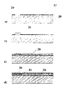
Fig. 2a) and 3a) each show a schematic cross- sectional view
of part of a semiconductor wafer representing the starting
point of the method according to the present invention. A
semiconductor wafer 20 is provided with a passivation layer
22 on a main surface thereof . Bond pads 24 are arranged in
the passivation layer 22. These bond pads 24 are normally
implemented as aluminium bond pads. The semiconductor wafer
20 consists preferably of silicon, the passivation layer 22
consisting of silicon nitride. Such a
semiconductor structure can be obtained from semiconductor
manufacturers in this form.
Making reference to Fig. 2, a preferred embodiment of the
method according to the first aspect of the present
invention will be explained in detail in the following.
Taking as a basis the starting substrate shown in Fig. 2a),
a chemical, i.e. currentless metal deposition on the
aluminium bond pad 24 is first carried out. By means of this
deposition, a metal bump 26 is produced on the bond pad 24,
as can be seen in Fig. 2b). It is apparent that, in
accordance with an arbitrary number of bond pads on the
semiconductor wafer, a large number of metal bumps can be
CA 02280904 1999-08-10
produced in this step. In order to realize the chemical
metal deposition, the aluminium bond pads must first be
subjected to an activation, e.g. a palladium activation.
In addition to chemical metal deposition, also photolitho-
graphic processes making use of a photoresist can be used
for producing the metal bumps.
According to the present embodiment, a dielectric is now
applied to the passivation 22 of the wafer 20; this
application can be carried out by means of stencil printing
(mask printing) or, alternatively, over the full area with
subsequent photolithographic structuring. Full-area
application of the dielectric comprises the steps of
applying a photomask in the manner known, exposing the bond
pad and the structures, which are not intended to constitute
conductor paths later on, and, subsequently, removing the
exposed areas.
Fig. 2c) shows the structure after the structuring of the
dielectric 28. The metal bump 26 and the dielectric 28
should only be separated by a small distance. Alternatively,
the metal bump and the dielectric 28 may slightly contact
each other. The dielectric 28 can, when applied, already be
activated for a subsequent chemical metallization, e.g. by
palladium particles. Alternatively, the dielectric can be
seeded in a wet-chemical process, e.g. by immersion in a
palladium-chloride solution, after its application.
As can be seen in Fig. 2c), the dielectric 28 has the same
height as the metal bump 26. This can be realized by
adjusting the application thickness of the dielectric
depending on the sequence of process steps used. It is,
however, also possible that the dielectric 28, when applied,
exceeds the metal bump 26 in height, and, in this case, it
will be necessary to etch the dielectric back to the height
of the metal bump after the application of the dielectric.
CA 02280904 1999-08-10
- 9 -
In a subsequent step, a chemical metal deposition is carried
out on the activated dielectric. In this chemical metal
deposition, gold, nickel, copper or palladium are deposited
on the activated dielectric and the metal bump in a current-
less deposition process so as to form a metallization layer
29. The chemically deposited metal and the metal bump grow
together thus forming an electrically conductive connection
from the metal bump to the metallization layer arranged on
the dielectric 28, whereby the electric connection from the
bond pad to the rewired area is realized. In the preferred
embodiment, a solder-stop lacquer with openings for the
planar pad arrangement is subsequently applied, the pads of
the pad arrangement being connected a . g . with edge pads by
the method according to the present invention.
Alternatively, the activated dielectric can be produced on
the areas of the passivation layer on which the structured
metallization is to be formed, by applying the dielectric
over the full area with the exception of the metal bumps and
by activating the areas to be metallized by exposure.
Making reference to Fig. 3, a preferred embodiment of the
method according to the second aspect of the present
invention will be explained in the following. Fig. 3a) again
shows the starting wafer 20 with the passivation layer 22
and the bond pad 24. A dielectric 30 is applied over the
full surface of the wafer 20 on which the passivation layer
22 is arranged. The dielectric 30 is structured, e.g. by
means of a photolithograpphic process, on the one hand for
uncovering the bond pad 24, and, on the other hand, for
defining the structure of the metallization which is to be
applied later on. The resultant structure is shown in Fig.
3b). Subsequently, the dielectric 30 and the bond pad 24 are
seeded preferably in a wet-chemical process, i.e. by
immersing the wafer in a palladium-chloride solution. A
metallization layer 32 is applied to the now existing
CA 02280904 1999-08-10
- 10 -
structure by means of chemical metal deposition. The
metallization layer is deposited on the activated dielectric
30 and on the activated bond pads 24 by the chemical metal
deposition, as can be seen in Fig. 3c). By means of the
method described with regard to Fig. 3, a contact can be
established, in one step and without any metal bump, between
the metal layer deposited on the dielectric and the bond pad
24.
The methods according to the present invention are
advantageous when a rewired area is produced on a chip. In
comparison with known methods, the present invention permits
such rewired areas to be realized at a more moderate price
and more rapidly, the number of process steps required being
simultaneously reduced.