Note : Les descriptions sont présentées dans la langue officielle dans laquelle elles ont été soumises.
CA 02282862 2000-09-07
SIGNAL-LEVEL COMPENSATION FOR COM1VIUNICATIONS CIRCUITS
FIELD OF THE INVENTION
The present invention relates to a circuit for communicating electronic
signals. In
particular, the present invention relates to a system for compensating for
signal level
variations in communications circuits.
BACKGROUND OF THE INVENTION
It is often desirable in communications circuits to compensate for variations
in power
supply voltages. It is also desirable to compensate for variations in
transistor
characteristics arising from changes in operating conditions, such as
temperature. These
features are particularly advantageous for low voltage applications, where a
variation in
power supply voltage and/or base-emitter voltage can cause output signal
voltages to vary
sufficiently so as to no longer comply with the appropriate signal
specification.
Attempts have been made at compensating for power supply voltage variations in
communications circuits where the input signals to the communications circuits
are
referenced to the power supply voltage. For instance, in one implementation, a
control
circuit monitors the power supply voltage and injects compensating currents
into the
communication circuit input stage to counter the effect of power supply,
variations on the
current levels in the input stage. However, such implementations are
unsuitable for high
frequency applications using low power supply voltages, since the injected
current can
cause the voltage drop across the current sink transistors coupled to the
input stage to
become undesirably low. Further, such implementations are ill-suited for
applications
where the power supply voltage is low or is susceptible to large variations,
since the
current sink transistors driving the input stage may become saturated. Also,
voltage
compensation at the input stage may leave insufficient head room for output
signal swing.
CA 02282862 2000-09-07
Accordingly, there remains in need for a system for compensating for signal
level
variations in communications circuits arising from variations in supply
voltage and/or
transistor characteristics.
SUMMARY OF THE INVENTION
According to the present invention, there is provided a signal level
compensating system
for communications circuits which addresses the deficiencies of the prior art.
The term
"communications circuit" is used herein in its generic sense as any circuit
which is
capable of conveying an electronic signal between an input and an output.
The signal level compensating system, according to the present invention,
comprises a
voltage-follower stage, a sensor and an output signal compensator. The voltage-
follower
stage includes a signal input for receiving an input signal, a signal output,
and at least one
transistor coupled between the signal input and the signal output for
providing an output
signal responsive to the input signal. The sensor provides a control signal
indicative of
variations in at least one of the power supply voltage and transistor
characteristics of the
transistor. The output signal compensator is coupled to the signal output and
provides an
compensator output signal responsive to the control signal for reducing the
impact of the
variations on the output signal.
In one aspect of the invention, the voltage-follower stage comprises a pair of
transistors
configured to receive differential input signals, and a resistive load stage
coupled to the
outputs of the voltage-follower transistors. The sensor comprises a transistor
matched to
?S the voltage-follower transistors and a resistor matched to the resistors of
the resistive load
stage, and provides control signals to the output signal compensator
representative of
variations in power supply voltage and voltage drop (eg. base-emitter, gate-
source) of the
voltage-follower transistors. The output signal compensator is coupled to the
sensor, and
comprises transistors configured as a current mirror coupled to the resistive
load stage.
-2-
CA 02282862 2000-09-07
The output current level provided by the output signal compensator is
responsive to the
control signal from the current sensor, and cancels variations in output sisal
at the
resistive load stage due to variations in power supply voltage and voltage
drop at the
voltage-follower stage.
In another aspect of the invention, the output of the voltage-follower stage
is coupled to a
pair of series-coupled differential voltage-followers for outputting the input
signals in
accordance with a desired signal specification. The sensor comprises
transistors matched
to the transistors of the voltage-follower stage and the series-coupled
voltage-followers,
and provides control signals to the output signal compensator representative
of variations
in power supply voltage and voltage drop (eg. base-emitter, gate-source) of
the transistors
of the voltage-follower stage and the series-coupled voltage-followers. The
output signal
compensator is coupled to the sensor and provides an output current responsive
to the
control signal from the current sensor, which cancels variations in output
signal voltage at
the output of the last of the series-coupled differential voltage-followers
due to variations
in power supply voltage and voltage drop of the transistors of the voltage-
follower stage
and the series-coupled voltage-followers.
In a preferred embodiment of the invention, the signal level compensating
system is
implemented as an integrated circuit on a single substrate, is powered by 3
volt power
source, and receives CML input signals from an emitter-follower output stage
external to
the integrated circuit. The voltage-follower stage comprises a pair of NPN
transistors,
and the current mirror comprises insulated nMOS transistors for allowing the
current
minor to operate below substrate voltage. The output of the voltage-follower
stage is
coupled to a pair of series-coupled emitter-followers for outputting the input
signals as
ECL output signals. The voltage-follower stage is coupled at its input to a
signal-
conditioner input stage which comprises a first differential buffer, a
differential voltage-
follower coupled to the output of the differential buffer, and a second
differential buffer
coupled to the output of the differential-emitter follower of the signal-
conditioner input
-3-
CA 02282862 2000-09-07
stage. The signal-conditioner input stage boosts the signal level of the input
signals to the
voltage-follower stage to provide sufficient headroom for compensating the
power supply
and base-emitter voltage variations.
BRIEF DESCRIPTION OF THE DRAWINGS
The preferred embodiments of the invention will now be described, by way of
example
only, with reference to the drawings, in which:
Fig. 1 is a schematic/block diagram of the signal-level compensating system
according to the present invention for receiving differential input signals
referenced to a
power supply voltage and for providing differential output signals, and
depicting the
voltage-follower stage, the sensor, and the output signal compensator;
Figs. 2a - 2j are schematic diagrams of various implementations of the sensors
shown in Fig.l;
Figs. 3a - 3d are schematic diagrams of various implementations of the output
signal compensator shown in Fig. l
Fig. 4 is a schematic diagram of a preferred implementation of a transient-
suppressing capacitor for use with the output signal compensators shown in
Fig. 3; and
Fig. 5 is a schematic diagram of a variation of the signal-level compensating
system shown in Fig. 1, including a signal conditioner input stage for
receiving CML
differential input signals from an external emitter-follower output, and an
output stage for
providing ECL differential output signals.
-4-
CA 02282862 2000-09-07
DETAILED DESCRIPTION OF THE PREFERRED EIVIBODIIVIENTS
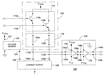
Turning to Fig. l, a signal-Level compensating communication system, denoted
generally
as 100, is shown comprising a voltage-follower stage 102, a sensor 104, an
output signal
compensator 106 and an output stage 108 all fabricated upon a common
integrated circuit
substrate. The signal-level compensating system 100 is shown being powered by
a
positive voltage source Vcco = 3 v, and a negative voltage source Vn. = Vn.o =
-2 v,
although other voltage references may be used. Further, the invention is not
limited to an
integrated circuit implementation but may also be implemented with discrete
components.
The voltage-follower stage 102 includes differential signal inputs 110a, 1 l
Ob for
receiving differential input signals referenced to a positive power supply
voltage, and
differential signal outputs 112a, 112b for providing differential output
signals responsive
to the input signals. However, it should be understood at the outset that the
invention is
not limited to differential signal applications, but could be applied to
single-ended
applications, if desired, although differential signals are preferred due to
their reduced
susceptibility to noise and parasitic effects.
The voltage-follower stage 102 comprises a differential emitter-follower 114
and a
?0 resistive-load stage 116 coupled to the differential outputs of the
differential emitter-
follower 114. The differential emitter-follower 114 comprises a pair of
identical NPN
transistors 118a, 118b, and the resistive-load stage 116 comprises a pair of
identical
resistors 120a, 120b. Alternately, the voltage-follower stage 102 may be
implemented as
with PNP transistors, or as a differential source-follower with FET
transistors, or with
any other transistor suitable for the intended application. Further, the
resistive-load stage
116 may comprise transistors configured to provide an impedance between the
differential outputs of the differential emitter-follower 114 and the
differential signal
outputs 112.
-5-
CA 02282862 2000-09-07
The sensor 104 includes a sensor input 122 for sensing variations in the
positive power
supply voltage and base-emitter voltage of the transistors employed in the
signal-level
compensating system 100, and a control output 124 for providing a control
signal
including information representing variations in the positive power supply
voltage and
the base-emitter voltages. However, it should be understood that the sensor
104 need not
sense both the positive power supply and base-emitter voltage variations in
all
applications, but might be used to sense only one of the positive power supply
and base-
emitter voltage variations where the output signal specification to be met is
sufficiently
forgiving.
Preferably, the sensor 104 also includes uIPN transistors (not shown) which
are matched
to the transistors 118 of the voltage-follower stage 102 and the transistors
of the output
stage 108 (discussed below), and resistors (not shown) which are matched to
the resistors
120 of the voltage-follower stage 102 and the resistors of the output stage
108.
Therefore, the control signal output by the sensor 104 includes information
representing
variations in the positive power supply voltage, and variations in the base-
emitter
voltages of the transistors of the voltage-follower stage 102 and the output
stage 108
arising from changes in operating conditions. The sensor 104 will be described
in greater
detail below with reference to Fig. 2.
?0
The output signal compensator 106 includes control input 126 for receiving the
control
signal output by the sensor 104, and a pair of signal outputs 128a, 128b, each
coupled to a
respective differential signal output 112 of the voltage-follower stage 102.
The signal
outputs 128 provide output signals which are responsive to the control signal
output by
the sensor 104, and are scaled to cancel or at least substantially reduce
variations in
output voltage of the output stage 108 resulting from variations in the
positive power
supply voltage and variations in the base-emitter voltages of the transistors
118 of the
voltage-follower stage 102 and transistors of the output stage 108. The output
signal
compensator 106 will be described in greater detail below with reference to
Fig. 3.
-6-
CA 02282862 2000-09-07
The output stage 108 comprises a first differential voltage-follower 130, and
a second
differential voltage-follower 132 which together provide differential output
signals
representative of the differential input signals input to the voltage-follower
stage 102 but
shifted to desired output signal levels. However, it should be understood that
the output
stage 108 is not an essential feature of the invention and may be eliminated
if the output
signals of the differential signal output 112 of the voltage-follower stage102
meet the
desired output signal specification. In such a case, therefore, the control
signal output by
the sensor 104 will not include information representing variations in the
base-emitter
voltages of the transistors of the output stage 108, and the outputs 128 of
the output
signal compensator 106 will provide output currents which are only scaled to
cancel or at
least substantially reduce variations in output voltage due to variations in
positive power
supply voltage and variations in the base-emitter voltages of the transistors
118 of the
voltage-follower stage 102. Further, the output stage 108 may comprise a
greater or
smaller number of voltage-followers as the output signal specification
required.
The first differential voltage-follower 130 of the output stage 108 includes a
first pair of
identical NPN transistors (not shown), a pair of differential inputs 134a,
134b, and a pair
of differential outputs 136a, 136b. Similarly, the second differential voltage-
follower 132
includes a second pair of identical NPN transistors (not shown), a pair of
differential
inputs 138a, 138b, and a pair of differential outputs 140a, 140b. The
transistors of the
first and second differential voltage-followers 130, 132 are matched as close
as possible
to the transistors of the sensor 104. The differential inputs 134 of the first
differential
voltage-follower 130 are each coupled to a respective differential signal
output 112, and
the differential inputs 138 of the second differential voltage-follower 132
are each
coupled to a respective differential output 136 of the first differential
voltage-follower
130.
Figs. 2a - 2j depict various implementations of the sensor 104. However, it
should be
understood at the outset that the sensor 104 is not limited to the variations
shown in Fig.
_7_
CA 02282862 2000-09-07
2, but includes any sensor capable of sensing changes in at least one of the
power supply
voltage, and transistor characteristics of the transistors of the voltage-
follower stage 102
and the first and second voltage-followers 130, 132.
Turning to Fig. 2c, a preferred implementation of the sensor 10-l is shown
comprising a
first diode-connected NPN transistor 202, a second diode-connected NPN
transistor 204
series-coupled to the first diode-connected NPN transistor 202, a first NPN
transistor-
based current minor 206 including a third diode-connected NPN transistor 208
series-
coupled to the second diode-connected NPN transistor 204, and a second nMOS
transistor-based current mirror 210 series-coupled to the current output of
the first current
mirror 206. The sensor 104 shown in Fig. 2c also includes a first resistor 212
in series
with the first and second diode-connected transistors 202, 204, a second
resistor 214
connected between the ground and the emitter of the third diode-connected
transistor 208,
and a third resistor 216 in series with the current output of the second
current mirror 210.
From the following discussion, it will become apparent that the sensor 104
only includes
three diode-connected transistors to sense changes in base-emitter voltage
drops of the
transistors 118, the transistors of the first differential voltage-follower
130, and the
transistors of the second differential voltage-follower 132. Therefore, it
should be
understood that the sensor 104 need not use three series-connected diode-
connected
transistors in all applications, but would preferably use the same number of
diode-
connected transistors as there are base-emitter voltage drops to be
compensated. Further,
the sensor 104 may comprise a mixture of transistor types (eg. PNP, NPN, FfiT)
corresponding to the transistors used in the voltage-follower 102, and the
output stage
108. Also, in applications where complete freedom from power supply and base-
emitter
(or gate-source) voltage variations is not required, the sensor 104 may use
fewer or more
diode-connected transistors than there are base-emitter voltage drops to be
compensated.
With the implementation shown in Fig. 1, the change in control signal output
current
-g-
CA 02282862 2000-09-07
produced by the sensor 104 will be:
!, V co - L~ ~e~ - ~ ~ez - :, ~e~
0 ~ ref
R212 'f" 8214
where: Dint - change in control output current
~V~~o - change in positive power supply voltage
~V~, - change in base-emitter voltage of transistor 202
~V,~2 - change in base-emitter voltage of transistor 204
~V,~3 - change in base-emitter voltage of transistor 208
R2,2 - resistance of resistor 212
Rz,~ - resistance of resistor 214
Preferably, the change in current output from each output 128 of the output
signal
compensator 106 is twice the change in output current produced by the sensor
104. With
1 ~ this design choice, the change in voltage drop across each resistor 120 of
the voltage-
follower stage 102 will be:
L1 VCCO - ~ ~1 - L1 ND02 - ~ ~3
~ V,zo = 2R,2o x
8212 + 8214
where: R,~o - resistance of resistor 120
By setting the resistance of each resistor 120 of the voltage-follower stage
102 as:
8212 + R2,4
R,zo = 2 ,
-9-
CA 02282862 2000-09-07
and by matching the resistors 212, 214 of the sensor 104 to the resistors 120
of the
voltage-follower stage 102, the change in voltage drop across each resistor
120 of the
voltage-follower stage 102 due to changes in output control current produced
by the
sensor 104 will be:
d V,2o = ~ U~~ - 0 ~, - ~ V6e2 - ~ ~3
Preferably, the transistors 118 of the voltage-follower stage 102 and the
transistors of the
output stage 108 are each completely matched to a respective diode-connected
transistor
202, 204, 208 of the sensor 104, and the resistors of the output stage 108 are
matched to
the resistors 212, 214 of the sensor 104. Alternately, the current density of
the transistors
118 of the voltage-follower stage 102 and the transistors of the output stage
108 may be
matched to a respective diode-connected transistor 202, 204, 208 of the sensor
104.
1~ Therefore:
~Vbel wbea~
wbe2 ~ V bc5 ~ and
wbe3 - OVbee for example)
?0 where: ~Vbe~ - change in base-emitter voltage of transistor 118
~VbeS - change in base-emitter voltage of voltage-follower 130
OVbe~ - change in base-emitter voltage of voltage-follower 132
and the change in output voltage at the differential outputs 140 of the output
stage 108,
25 due to changes in positive power supply voltage and base-emitter voltages,
will be:
o v,4o = o v~~o - o ~. - o ~5 - o ~6 - o v,2o = o
-10-
CA 02282862 2000-09-07
Alternately, the foregoing result may be obtained even if the transistors 118
of the
voltage-follower stage 102 and the transistors of the output stage 108 are not
matched to a
respective diode-connected transistor 202, 204, 208 of the sensor 104, if the
following
condition is met:
~Vbet + ~Vbc, T wbc3 - ~Vbe4 + ~VbcS + wbc6
As discussed above, preferably the change in current output from each output
128 of the
output signal compensator 106 is twice the change in output current produced
by the
sensor 104. From the foregoing calculations, it will be apparent that this
design choice
reduces the power consumption of the voltage sensor 104. Further, this design
choice
increases the speed of the circuit. However, other current ratios of the
output signal
compensator 106 may be used, provided a suitable change is made to the ratio
of the
resistor 120 to the sum R2,2 + R,,~.
As discussed above, preferably at least the current density of the transistors
118 of the
voltage-follower 102 and the transistors of the first and second differential
voltage-
followers 130, 132 are matched as close as possible to respective diode-
connected
transistors of the sensor 104. However, it will be appreciated that, in order
for the signal
compensating system 100 to compensate for output signal variations, the
current densities
of the transistors 118 and the transistors of the first and second
differential voltage-
followers 130, 132 need only be equal to the current density of the respective
transistors
of the sensor 104. -In this latter variation, the signal-level compensating
system 100 may
not completely cancel variations in output signal voltage at the differential
outputs 140
unless, although the uncompensated variation will be negligible. Further, it
is believed
that the current densities need not be matched to compensate for output signal
variations,
although the performance of such a system may be inferior to a system
employing
matched transistors or a system employing transistors of matching current
densities.
CA 02282862 2000-09-07
The remaining implementations of the sensor 104 shown in Figs. 2a to 2j are
substantially similar in operation to the sensor 104 shown in Fib. 2c, but
with some minor
differences. For instance, since the transistor of the output signal
compensator 106
connected to control input 126 has its source terminal below substrate voltage
(to be
discussed below) and the transistors of the second current mirror 210 are
referenced to
Vcco~ the sensor 104 shown in Fig. 2c includes a resistor 216 in series with
the current
output of the second current minor 210 in order to provide over-voltage
protection for the
second current mirror 210. Further, the resistor 216 also reduces the
possibility of noise
from the positive power supply. However, as shown in Fig. 2d, the sensor 104
may
include instead a nMOS transistor 218 cascode-connected with the output of the
current
mirror 210, instead of the resistor 214, or may include both a resistor 216
and a MOS
cascode-connected transistor 218, as shown in Fig. 2e.
The sensors 104 shown in Fig. 2f and Fig. 2 j are substantially identical to
the sensors 104
respectively shown in Fig. 2e and Fig. 2d, except that the nMOS cascode-
connected
transistors 218 are replaced with PNP cascode-connected transistors.
Similarly, the
second current minors 210 of the sensors 104 shown in Fig. 2e and Fig. 2d
comprise
nMOS transistors, whereas the second current minors 210 of the sensors 104
shown in
Fig. 2h and Fig. 2i comprise PNP transistors. The sensor 104 shown in Fig. 2j
will be
described below.
The sensor 104 shown in Fig. 2a and Fig. 2b are simpler implementations of the
sensor
104. For instance, the sensor 104 shown in Fig. 2a includes two diode-
connected NPN
transistors and one nMOS transistor all connected in series. This variation
has the
advantage of reduced power consumption over the other implementations since
only one
current is drawn from the positive power supply. However, as this variation
assumes that
the Vbs voltage drop of the nMOS transistor will be approximately equal to one
base-
emitter voltage drop, there may be slight reduction in performance if VAS does
not
accurately track a base-emitter voltage drop. The sensor shown in Fig. 2b is
similar to the
-12-
CA 02282862 2000-09-07
sensor 104 shown in Fig. 2a, eYCept that the variation shown in Fig. 2b uses a
PNP
transistor in replacement of the nNlOS transistor and may, therefore, also
suffer from a
slight reduction in performance.
Figs. 3a - 3d depict various implementations of the output signal compensator
106.
However, it should be understood at the outset that the output signal
compensator 106 is
not limited to the variations shown in Fig. 3, but includes any output signal
compensator
capable of cooperating with the voltage-follower stage 102 so as to reduce
variations in
output signal arising from variations in power supply voltage or transistor
characteristics.
Turning to Fig. 3a, a preferred implementation of the output signal
compensator 106 is
shown configured as a current mirror, and comprising a diode-connected master
transistor
302, a first slave transistor 304, and a second slave transistor 306 coupled
to the master
transistor 302. Since the output voltage at the signal outputs 112 of the
voltage-follower
1 ~ stage 102 will vary in accordance with the input signals delivered to the
signal inputs 110
of the voltage-follower stage 102, the output signal compensator 106 also
includes a first
cascode-connected transistor 308a connected to the current output of the first
slave
transistor 304, and a second cascode-connected transistor 308b connected to
the current
output of the second slave transistor 306 to reduce the impact of the changes
in output
?0 voltage at the signal outputs 112 on the current magnitude of provided by
the first and
second slave transistors 304, 306. However, as will be apparent below, the
first and
second cascode-connected transistors 308 are not essential, and may be
eliminated in
applications where the desired output signal specification of the signal-level
compensating system 100 is sufficiently forgiving.
The transistors 302, 304, 306, 308 of the current minor 106 are operated below
substrate
voltage to increase the headroom available at the differential signal outputs
112 of the
voltage-follower stage 102 for voltage compensation. As a result, the
transistors 302,
304, 306, 308 comprise insulated nMOS transistors, although it is believed
that any
-13-
CA 02282862 2000-09-07
transistor which can operate with its collectoridrain terminal below substrate
voltage can
also be used.
The output signal compensator 106, shown in Fig. 3a, includes a shunt
capacitor
connected across the gate-source terminals of the cascode-connected
transistors 308 to
reduce the impact on the cascode-connected transistors 308 of noise from the
power
supply and transients. The output signal compensator 106, shown in Fig. 3a,
also
includes a capacitive circuit 310 connected across the master transistor 302
to reduce the
impact of power supply noise on the output current characteristics of the
output signal
compensator 106. As shown in Fig. 4, since the capacitive circuit 310 is
required to
operate below substrate voltage, preferably the capacitive circuit 310
comprises an
insulated nMOS transistor whose gate terminal is connected to the gate and
drain
terminals of the master transistor 302, and whose drain and source terminals
are
connected to the source terminals of the transistors 302, 304, 306.
The remaining implementations of the output signal compensator 106 shown in
Figs. 3b
to 3d are substantially similar in operation to the output signal compensator
106 shown in
Fig. 3a, but with some minor differences. For instance, the output signal
compensators
106 shown in Fig. 3b and Fig. 3d lack the cascode-connected transistors 308,
and the
output signal compensators 106 shown in Fig. 3c and Fig. 3d include resistors
312a, 312b
each in series with a respective output transistor and a respective signal
output 128 for
signal shaping.
Numerous variations upon the signal-level compensating system 100 may be
realized.
For instance, as discussed above, the signal-level compensating system 100 may
be
configured to receive a differential or a single-ended communication signal.
The value of
the resistor 120 of the voltage-follower stage 102 and the current gain of the
current
mirror 106 may be adjusted to vary the degree and speed of compensation, and
to adjust
the power dissipation of the compensating system 100. The number of voltage-
follower
-14-
CA 02282862 2000-09-07
stages of the output stage 108 may be varied in accordance with the degree of
level
shifting required to meet the output signal specification. Further, although
it is believed
that having voltage compensation occur before the signal reaches the output
stage 108
allows the power dissipation through the resistors 120 to be reduced, it is
also believed
that the output of the current mirror 106 may be relocated so as to allow
voltage
compensation to take place at one of the voltage-followers of the output stage
108. Also,
it is believed that if the output signal specification is defined by changes
in current levels,
rather than changes in voltage levels, the resistive-load stage 116 may be
eliminated and
the voltage-follower stages replaced with current follower stages so as to
provide output
signals which are substantially free of current variations which might
otherwise be caused
by variations in positive power supply or base-emitter transistor voltages.
Turning to Fig. 5, a preferred implementation of the signal-level compensating
system,
denoted generally as 200, is shown comprising the voltage-follower stage 102,
the sensor
104, the output signal compensator 106 and the output stage 108 of Fig. 1; and
a signal-
conditioner input stage 160, and a band-gap voltage reference 162 all
fabricated upon a
common integrated circuit substrate. The signal-level compensating system 200
is
particularly advantageous since it allows the amount of output signal swing of
the output
stage 108 to be set independently of the amount of compensation. Further, the
signal-
level compensating system 200 boosts the signal level of the input signals
transmitted to
the voltage-follower stage 102 so as to allow the circuit 200 to receive input
signals
whose logic high voltage levels are a base-emitter voltage drop below positive
power
supply voltage (such as where an external emitter-follower output stage is
used) without a
reduction in voltage compensation capabilities.
The output stage 108 comprises a first differential voltage-follower 130, and
a second
differential voltage-follower 132 which together provide differential output
signals
representative of the differential input signals applied to the voltage-
follower stage 102
but shifted to ECL levels. The first differential voltage-follower 130
includes a first pair
-15-
CA 02282862 2000-09-07
of identical NPN transistors l~Oa, 150b configured as emitter-followers, a
pair of
differential inputs 134a, 134b, and a pair of differential outputs 136a, 136b.
Similarly,
the second differential voltage-follower 132 includes a second pair of
identical NPN
transistors 152x, 1~2b configured as emitter-followers, a pair of differential
inputs 138a,
138b, and a pair of differential outputs 140a, 140b. Alternately, the first
and second
voltage-followers 130, 132 may be implemented as a differential source-
followers with
MOS transistors, or with any other transistor suitable for the intended
application.
As discussed above, the transistors 150, 152 are matched as close as possible
to the
respective transistors of the sensor 104. The differential inputs 134 of the
first
differential voltage-follower 130 are each coupled to a respective
differential signal
output 112, and the differential inputs 138 of the second differential voltage-
follower 132
are each coupled to a respective differential output 136 of the first
differential voltage-
follower 130. As will be apparent, the first differential voltage-follower 130
reproduces
the output signal of the differential signal output 112 but shifted down in
voltage by one
base-emitter voltage drop. Similarly, the second differential voltage-follower
132
reproduces the output signal of the first differential voltage-follower 130
but shifted down
in voltage by another base-emitter voltage drop.
?0 The signal-conditioner input stage 160 includes differential signal inputs
164a, 164b for
receiving CML input signals from an emitter-follower stage (not shown) of a
circuit
external to the integrated circuit, and differential signal outputs 166a, 166b
for providing
an output signal responsive to the input signals, and comprises a first
differential buffer
168 coupled at its differential inputs to the differential signal inputs 164,
a differential
voltage-follower 170 coupled to the first differential buffer 168, a second
differential
buffer 172 coupled to the differential voltage-follower 170, and a current
sink 174
coupled to the differential buffers 168, 172 and the differential voltage-
follower 170.
The first differential buffer 168 comprises a pair of identical NPN
transistors 176a, 176b,
-16-
CA 02282862 2000-09-07
and a pair of identical resistors 178a, 178b having a common connection point
at one end
and being connected to a respective collector at the other end. The first
differential buffer
168 also includes a resistor R~ connected between the positive power supply
and the
common connection point of the resistors 178 to shift the output voltage of
the first
differential buffer 168 downwards a ti:ced amount to meet the output signal
specification,
if necessary.
The differential voltage-follower 170 comprises a pair of identical NPN
transistors 180a,
180b, configured as emitter-followers, whose collectors are connected to the
positive
power supply, and whose bases are each connected to a respective collector of
the
transistors 176 of the first differential buffer 168.
The second differential buffer 172 comprises a pair of identical NPN
transistors 182a,
182b whose bases are each connected to a respective emitter of the transistors
180 of the
1 ~ differential voltage-follower 170, and whose collectors are each connected
to a respective
signal input 110 of the voltage-follower stage 102. The second differential
buffer 172
also includes a pair of identical resistors 184a, 184b each being connected
between the
positive power supply and a respective collector of the transistors 182.
The current sink 174 comprises a first NPN transistor 186 whose collector is
connected to
the emitters of the transistors 176 of the first differential buffer 168, a
pair of matched ,
NPN transistors 188 (comprising transistors 188a, 188b) whose collectors are
each
connected to a respective emitter of the transistors 180 of the differential
voltage-follower
170, and a triplet of matched NPN transistors 190 (comprising transistors
190a, 190b,
190c) whose collectors are connected in common to the emitters of the
transistors 182 of
the second differential buffer 172. The current sink 174 also includes a
plurality of
matched resistors 192, with each resistor 192 being connected between a
respective
emitter of the transistors 186, 188, 190 and ground. As will be appreciated,
the first and
second differential buffers 168, 172, the differential voltage-follower 170
and the current
-17-
CA 02282862 2000-09-07
sink 174 may be implemented using FET transistors, or any other suitable
transistor.
The band-gap voltage reference 162 includes a voltage-follower configured
output
transistor (not shown) which is matched to the transistors 186, 188, 190, and
an emitter
resistor (of resistance R) connected between the emitter terminal of the
output transistor
and ground and matched to the resistors 192 of the current sink 174. The base
output of
the output transistor is connected to the bases of the transistors 186, 188,
190, and biases
the transistors 186, 188, 190 with a voltage of:
~~ _ ~+ VR
where: Vb;~ = output voltage of the voltage reference 162
V~ - base-emitter voltage of voltage-follower transistor of the
voltage reference 162
VR - constant voltage drop across the emitter resistor of the
voltage reference 162
The resistance of each of the resistors 192 is equal to the resistance R of
the emitter
resistor. Therefore, the collector current of each of the transistors 186a,
186b, 186c,
188a, 188b, 190a, 190b,190c of the current sink 174 will remain at:
Ic = -
where: i~ - collector current of the transistors 186, 188, 190
The voltage drop across the resistor 184 when the corresponding transistor 182
of the
second differential buffer 172 is in the conducting state will then be:
-18-
CA 02282862 2000-09-07
~V,a~ = 3~* R,a~
R
where: ~V,B,, = voltage drop across the resistor 184
R,84 - resistance of the resistor 184
With the ECL signal specification requiring output voltage to be between
approximately -
0.5 v and -1.0 v for logical high and between approximately -1.6 v and -2.0 v
for logical
low, it is desirable for the signal-level compensating system 200 to maintain
the voltage
at the output of the output stage 108 at approximately -0.8 v for logical high
at
approximately -1.8 v for logical low. Since this design choice requires an
output signal
swing of approximately 1.0 v, ~V,84 will be approximately 1.0 volts.
Therefore, with a
positive power supply voltage of 3.0 volts, the output voltage of the
differential buffer
172 will be at least 2.0 v, thereby preventing saturation of the transistors
186, 188, 190 of
the current sink 174 and providing a sufficiently large V~e voltage drop
across the
transistors 182 of the differential buffer 172 to allow high frequency
operation of the
signal-level compensating system 200.
The discussion of the desired voltage swing OV,g, assumed that the current
drawn by the
transistors of the output stage 108 will remain constant, independent of the
output voltage
of the output stage 108. However, in practice, the current density of the
transistors of the
output stage 108 will be greater when the output voltage of the output stage
108 is at the
upper output voltage, and will be less when the output voltage of the output
stage 108 is
at the lower output voltage. Thus, if the signal-level compensating system 200
is
designed to maintain the voltage at the output of the output stage 108 at
approximately -
0.8 v for logical high, the voltage at the output of the output stage 108 will
be slightly
greater (less negative) than the desired -1.8 v for logical low even though
OV,g4 is set at
1.0 v. Similarly, if the signal-level compensating system 200 is designed to
maintain the
voltage at the output of the output stage 108 at approximately -1.8 v for
logical low, the
voltage at the output of the output stage 108 will be slightly less (more
negative) than the
-19-
CA 02282862 2000-09-07
desired -0.8 v for logical high. To correct for this variation, the resistance
of the resistor
R~s4 may be increased slightly to increase the voltage swing OV,s, to the
output stage 108.
Other modifications may be undertaken to adjust the output voltage of the
output stage
108 by a set amount. For instance, as shown in Fig. 2j, the output signal
compensator
106 may be modified to include a bypass transistor 220 in series with a bypass
resistor
222, with the bypass transistor 220 and resistor 222 being in parallel with
the diode-
connected transistors 202, 204, 208, and the resistor being of the same type
as the
resistors 120. The bypass transistor 220 is biased from the band-gap voltage
reference
162 and, therefore, can be used to trim the compensation current produced by
the current
mirror 106 so as to shift upwards the output voltage of the voltage-follower
stage 102.
Alternately, the by-pass transistor 220 and resistor 222 may be connected in
parallel with
the output of the second current minor 210. On the other hand, in order to
shift
downwards the output voltage of the voltage-follower stage 102, the by-pass
transistor
220 and resistor 222 may be connected in parallel with the output of the first
current
minor 206 so as to increase the compensation current produced by the current
mirror 106.
Other means for adjusting the output voltage of the output stage 108 will be
apparent to
those skilled in the art.
As will be appreciated, without the signal-conditioner input stage 160, the
input signals
received at the differential signal inputs 110 of the voltage-follower stage
102 of the
signal-level compensating system 200 would be one base-emitter voltage drop
lower, due
to the external voltage-follower driving the signal-level compensating system
200, than
the input signals received at the differential signal inputs 110 of the
voltage-follower
stage 102 of the signal-level compensating system 100. Accordingly, the signal-
conditioner input stage 160 is desirable, particularly for low voltage
applications since,
absent the signal-conditioner input stage 160, the transistors 190 may become
saturated.
Further, it will also be apparent from the foregoing discussion that the
voltage swing at
-20-
CA 02282862 2000-09-07
the signal outputs 140 of the output stage 108 is determined by the ratio of
the resistance
R,84 of the resistors 184 of the second differential buffer 172 to the
resistance R of the
resistors 192 of the current source 174, whereas the degree of voltage
compensation is
related to the current gain of the current mirror 106, and the ratio of the
resistance R,ZO of
the resistors 120 of the voltage-follower stage 102 to the resistance R,,~,
R,,~ of the
resistors 212, 214 of the sensor 104. Therefore, it will be appreciated that
the signal-level
compensating system 200 has the notable advantage of allowing the degree of
voltage
compensation to be set independently of the desired output voltage swing.
The description of the foregoing embodiments is intended to be illustrative
and not
exhaustive of the present invention. Those of ordinary skill will realize
certain additions,
deletions and/or modifications to the embodiments described herein which
nevertheless
will not depart from the spirit or scope of the present invention, as defined
by the claims
appended hereto.
-21-