Note : Les descriptions sont présentées dans la langue officielle dans laquelle elles ont été soumises.
CA 02283383 1999-09-03
WO 98/44768 PCT/GB97/03560
- 1 -
METHOD OF ARRANGING SIGNAL AND DESTINATION ,PADS TO PROVIDE
MULTIPLE SIGNAL/DESTINATION CONNECTION C~INATIONS
The present invention relates generally to electronic
circuits. More particularly, the present invention relates
to a method of arranging signal and destination pads in
electronic circuits to provide multiple signal/destination
connection configurations.
1o In electronic circuits, components are attached to a
substrate and the inputs and outputs of the components are
interconnected by wires or, more typically, circuit traces.
Circuit traces electrically connect an output terminal, or
signal origination, of one component to an input terminal,
or signal destination, of another component. An individual
circuit trace may consist of a single path having only one
origination and one destination, or it may be branched so as
to have multiple originations and/or destinations. In
either case, each end of a circuit trace usually terminates
2o in a pad, to which a component input or output terminal is
attached.
When a circuit is designed, it is generally laid out
such that each of the components may be oriented in only one
way on the circuit substrate. However, it may sometimes be
desired to lay out a circuit such that one or more
components may be oriented in more than one way, so that
more than one configuration of signal/destination
connections can be made using a single circuit trace layout.
This idea is illustrated in FIG. 1. Here, a signal circuit
3o trace 20 having two signal pads 21/22, and two destination
circuit traces 30/35 each having one destination pad 31/36,
respectively, have been laid out on a substrate 50. The
signal trace 20 is attached at one end to an output terminal
CA 02283383 1999-09-03
WO 98/44768 PCT/GB97/03560
- 2 -
(signal origination) of an electronic component, while the
destination traces 30/35 are each attached to an input
terminal (signal destination) of another component.
Although these components and their terminals are not shown,
the signal originations are denoted by single-digit
reference numerals 1, 2, 3, and so forth, and the signal
destinations are denoted by reference letters A, B, C, and
so forth.
Once the circuit traces 20/30/35 have been laid out on
the substrate 50 as shown in FIG. 1, the circuit can then be
populated with components. At this point, the substrate
populator has the option of attaching a jumper 10 (1)
between signal pad 21 and destination pad 31, thereby
connecting signal 1 with destination A, or (2) between
signal pad 22 and destination pad 36 (as indicated by the
dashed outline of a jumper 10), thereby connecting signal 1
with destination B. In either combination, a unique circuit
is produced. Thus it can be seen that a single circuit
trace arrangement may be populated with jumpers 10 in mo=a
2o than one way so as to provide more than one
signal/destination connection comb~natie~ (hereinafter
referred to as an "SDCC"). This m~ ns t rather t~:ar
producing two separate circuit trace arru ~ments -- e.g.,
two unpopulated printed circuit boards (PC -- which have
similar layouts except for a few signal/de~ ration
connections, it is possible to use the forec -gig
multiconfigurable pad arrangement to produce e:~ly one such
circuit trace/PCB which has the possibility of producing
either of two SDCCs. In short, one circuit/PCB using the
3o foregoing pad arrangement can take the place of two separate
but similarly laid out circuits/PCBs.
FIG. 1 illustrates a prior art attempt at providing
more than one SDCC for one signal origination~l and two
CA 02283383 1999-09-03
WO 98/44768 PCT/GB97/03560
- 3 -
potential destinations A/B. This arrangement offers two
possible SDCCs: 1A (i.e., signal 1 to destination A) and 1B.
FIG. 2 illustrates the prior art case for two signals 1/2
and two destinations A/B, which also provides two possible
connection combinations: 2A/2B and 1B/2A. FIG. 3
illustrates an arrangement of three signals 1/2/3 and three
destinations A/B/C, which once again offers two possible
connection combinations: lA/2B/3C and 1B/2C/3A.
Several things should become apparent from the
io arrangements presented in FIGS. 1-3. First, the layout of
the signals and destinations may be re-arranged in many
different ways to achieve the same result. For example,
FIG. 4 illustrates one of the many ways in which the three
signals 1/2/3 and three destinations A/B/C of FIG. 3 may be
re-arranged to produce the same two possible SDCCs as FIG.
3. Second, the signals and destinations may be arranged so
as to present different sets of two SDCCs. To illustrate
this, note that with three signals and three destinations,
3-factorial, or six, SDCCs are possible in all:
I II III IV V VI
lA lA 1B 1B 1C 1C
2B 2C 2A 2C 2A 2B
3C 3B 3C 3A 3B 3A
(This assumes, of course, that each signal is connected
to one and only one unique destination, and vice versa.)
However, although three inputs and three outputs can be
arranged in six different SDCCs, only two may be provided
. 30 for according to the foregoing pad arrangement without
adding additional pads. FIG. 5 illustrates one way of
arranging the same three signals 1/2/3 and destination pads
A/B/C to provide two different SDCCs: 1B/2A/3~ and 3.C/2A/3B.
CA 02283383 1999-09-03
WO 98/44768 PCT/GB97/03560
- 4 -
Third, it should become apparent that the number of signals
does not have to equal the number of destinations. For
example, FIG. 1 presents the case of one signal 1 and two
destinations A/B. Fourth, note that an arrangement having n
signals and at least n destinations requires the use of 4n
pads. Thus, in FIG. 1 where n = 1, four pads are required.
In FIG. 2 where
n = 2, eight pads are needed, and in FIGS. 3-5 where
n = 3, twelve pads are needed.
Furthermore, several assumptions underlie the prior art
arrangements shown in FIGS. 1-5. First, each signal
origination and each signal destination may have multiple
pads, but each signal must ultimately connect with one and
only one signal destination, regardless of which particular
pads are jumpered together; likewise, each signal
destination must ultimately connect with one and only one
signal origination. Second, each signal pad may be
connected to no more than one destination pad, and vice
versa. Third, each signal or destination pad can have no
more than one jumper attached to it. Fourth, jumpers may
not cross one another.
Another prior art approach which is an improvement upon
the aforementioned one signal-two destination arrangement of
FIG. 1, and which also relies upon the assumptions discussed
above, is illustrated in FIG. 6. This approach differs from
the one pictured in FIG. 1 in that (1) the two signal pads
21/22 and their associated branches have been combined to
form only one signal pad 23 and one branch, and (2) the
signal pad 23 has been interposed between the two
destination pads 31/36. This combination and interposition
allows a jumper 10 to be placed either between signal 1 and
destination A, as shown in FIG. 6, or between signal 1 and
destination B, as represented by the dashed outline. Thus,
CA 02283383 1999-09-03
WO 9$/44768 PCT/GB97/03560
- 5 -
this improved approach allows the same connection
combinations as allowed by FIG. 1, but with the added
benefit of requiring only three pads rather than four,
thereby taking up Less space on the substrate 50.
Although the foregoing prior art approaches are
effective ways of arranging signal and destination pads so
as to provide multiple SDCCs, they nonetheless suffer some
serious drawbacks. First, the methods illustrated in FIGS.
1-5 take up a lot of space on the substrate. Second, these
l0 methods provide an undesirable dangling signal trace for
each signal in either of the two possible connection
combinations. For example, when the jumpers are positioned
as shown in FIG. 2, signal pads 22 and 27 and their
associated branches form dangling signal traces for signals
1 and 2, respectively. Likewise, when the alternate,
dashed-line connections are made in FIG. 2, pads 21 and 26
and their associated branches form dangling traces. (The
arrangements shown in FIGS. 3-5 also leave a dangling trace
for each signal 1/2/3.) These dangling traces may act as
unwanted RF transmitters or receivers, thus interfering with
the electrical function of elements within the circuit or
with other circuits and equipment in the surrounding
environment. As for the approach shown in FIG. 6, dangling
traces have been eliminated and the number of pads reduced,
but its application has been limited to cases involving only
one signal and two possible destinations.
It is desirable, therefore, to provide a way of
arranging signal and destination pads on a substrate for
multiple (i.e., two or more) signals and an equal or greater
~ 3o number of destinations so as to provide multiple SDCCs while
eliminating dangling traces and reducing the overall number
of pads required.
CA 02283383 1999-09-03
WO 98/44768 PCT/GB97/03560
- 6 -
According to a first aspect of the present invention,
there is provided an electronic circuit assembly having
multiple signal/destination connection combinations,
comprising n signal pads and n destination pads, where n is
a number greater than one, said signal pads and said
destination pads being arranged columns on a substrate in a
polygonal array in an alternating signal pad/destination pad
pattern.
According to a second aspect of the present invention,
there is provided an electronic circuit assembly having
multiple signal/destination connection combinations,
comprising n signal pads and n+1 destination pads, where n
is a number greater than one, said signal pads and said
destination pads being arranged on a substrate in a linear
array, wherein a first endmost pad of said array is a first
destination pad, a next closest pad in said array is a first
signal pad, a next closest pad in said array is a second
destination pad, and so forth in an alternating signal
pad/destination pad pattern, wherein a second endmost pad in
said array is a last destination pad.
According to a third aspect of the present invention,
there is provided an electronic circuit assembly having
multiple signal/destination connection combinations,
comprising a first circuit trace having first and second
destination pads thereon, a second circuit trace having
third and fourth destination pads thereon, a first signal
pad positioned so as to be connectable by a jumper to either
of said first and third destination pads, and a second
signal pad positioned so as to be connectable by a jumper to
either of said second and fourth destination pads,
wherein said destination pads and said signal pads are
arranged on a substrate.
c~y~E~~~o ~ ANr~u~.~
CA 02283383 1999-09-03
WO 98/44768 PCT/GB97/03560
It is an advantage that the number of pads required to
provide multiple SDCCs for two or more signals in the
embodiments of the present invention is significantly
reduced as compared to the prior art.
It is a further advantage that the embodiments of the
present invention provide multiple SDCCs for two or more
signals while completely eliminating dangling signal traces.
Another advantage is the provision of a higher number
of possible SDCCs for each arrangement of two or more
signals as compared to the prior art.
Yet another advantage is that the applicability to a
wide range of applications, including printed circuit
boards, microelectronics, and integrated circuit
applications.
The invention will now be described further, by way of
example, with reference to the accompanying drawings, in
which:
FIG. 1 is a top plan view of a circuit portion having
one signal and two destinations according to the prior art;
FIG. 2 is a top plan view of a circuit portion having
two signals and two destinations according to the prior art;
FIG. 3 is a top plan view of a circuit portion having
three signals and three destinations according to the prior
art;
FIG. 4 is a top plan view of an alternative version of
a circuit portion having three signals and three
destinations according to the prior art;
FIG. 5 is a top plan view of another alternative
version of a circuit portion having three signals and three
. 30 destinations according to the prior art;
FIG. 6 is a top plan view of a circuit portion having
one signal and two destinations according to an improvement
within the prior art;
CA 02283383 1999-09-03
WO 98/44768 PCT/GB97/03560
- g -
FIGS. 7-8 are top plan views of circuit portions
according to a first embodiment of the present invention
having, respectively, 2 signals/2 destinations and
3 signals/3 destinations;
FIGS. 9-10 are top plan views of circuit portions
according to a second embodiment of the present invention
having, respectively, 2 signals/2 destinations and
3 signals/3 destinations;
FIGS. 11-12 are top plan views of alternative versions
io of the embodiment shown in FIG. 10;
FIGS. 13-14 are top plan views of circuit portions
according to a third embodiment of the present invention
having, respectively, 2 signals/2 destinations and
3 signals/3 destinations;
FIGS. 15-16 are top plan views of circuit portions
according to a third embodiment of the present invention
having 4 signals/4 destinations; and
FIG. 17 is a top plan view of a circuit portion
according to a fourth embodiment of the present invention
having 2 signals/2 destinations.
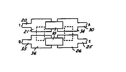
Referring now to the drawings, FIG. 7 shows a first
embodiment of the present invention, comprising n signal
pads and n+l destination pads, where n is a number greater
than one. FIG. 7 illustrates the case where n = 2. Signals
1 and 2 are carried by circuit traces 20 and 25,
respectively, which terminate in signal pads 21 and 26,
respectively. Signal destinations A and B are connected to
circuit traces 30 and 35, respectively, which terminate in
3o destination pads 31 and 36/37, respectively. The signal
pads 21/26 and destination pads 31/36/37 are arranged on a
substrate 50 in a linear array, wherein a first endmost pad
of the array is a first destination pad 36, a next closest
CA 02283383 1999-09-03
WO 98/44?68 PCT/GB97/03560
_ g _
pad in the array is a first signal pad 21, a next closest
pad in the array is a second destination pad 31, and so
forth in an alternating signal pad/destination pad pattern,
wherein a second endmost pad in the array is a last
destination pad 37.
The foregoing example illustrates one way in which the
respective pads of two signals 1/2 and two destinations A/B
may be arranged according to a first embodiment of the
present invention. However, other specific arrangements are
to possible using these same signals 1/2 and destinations A/B.
For example, the positioning of signals 1 and 2 may be
reversed, such that signal 1 is carried by trace 25 and
signal 2 is carried by trace 20, and/or destinations A and B
may be reversed such that destination A is connected to
trace 35 and destination B is connected to trace 30. Thus,
what is important is the arrangement and pattern of the
signal and destination pads, rather than the order or
arrangement of the respective signals and destinations to
which the pads are connected. For example, in the present
2o embodiment it is important that the first endmost pad in the
array be a first destination pad (as opposed to a signal
pad), not that it be connected by a circuit trace to any
particular destination.
As shown in FIG. 7, the last destination pad 37 may
have a signal destination B in common with that of the first
destination pad 36. This arrangement offers two possible
SDCCs: lA/2B and 1B/2A, depending upon how jumpers 10 are
positioned. Alternatively, the last destination pad 37 may
be connected to a unique destination C (not shown) this
would offer possible SDCCs of lA/2C and 1B/2A. Thus, it
should become apparent that for a given n, there may be
either n or n+I destinations to which the destination pads
are connected, depending, respectively, on whether the last
CA 02283383 1999-09-03
WO 98/44768 PGT/GB97/03560
- 10 -
destination pad 37 is connected to a repeated destination
(e.g., B) or to a unique destination(e.g., C).
FIG. 8 illustrates the case where n = 3. As in FIG. 7,
note the alternating destination pad/signal pad pattern,
which utilises n signal pads 21/26/41 and nf1 destination
pads 46/31/36/47: It should also be noted that in the
present embodiment (1) each signal pad is electrically
connected to a unique (non-repeated) signal origination (in
order to avoid dangling traces), (2) the arrangement
1o provides two possible SDCCs, and (3) n jumpers are arranged
so as to connect each signal pad to only one destination pad
and each destination pad to only one signal pad.
FIGS. 7 and 8 illustrate the case where the linear
array of signal and destination pads is laid out in a
substantially straight line. It should also be noted that
the linear array may be laid out in a substantially stair-
step-shaped line, giving rise to a second embodiment of the
present invention. This is illustrated in FIGS. 9 and 10
for the cases of n = 2 and n = 3, respectively. The
2o clustered, stair-step arrangement of this embodiment has an
advantage over the linear arrangement of the first
embodiment in that its length L is generally shorter, albeit
its width W is generally wider. Also note that whereas in
the first embodiment all of the jumpers 10 are oriented
substantially along a straight line in either of the two
possible SDCCs, in FIGS. 7 and 8 the jumpers 10 are arranged
either all "horizontally" in one SDCC (as pictured in FIGS.
9 and 10) or all "vertically" in the other SDCC (as
represented by the dashed jumper outlines).
3o FIGS. 11 and 12 illustrate alternative examples of pad
layouts for the case of n = 3 according to the substantially
stair-step-shaped linear array of the present embodiment.
As in FIG. 10, these two arrangements provide SDCCs of
CA 02283383 1999-09-03
WO 98/44768 PCT/GB97/03560
- 11 -
lA/2B/3C and 1C/2A/3B, yet all three arrangements are
different in layout. This illustrates how the circuit
designer has multiple pad configurations at his or her
disposal for a given number of signals and destinations, yet
with all providing the same possible SDCCs. This allows the
circuit designer to lay out the circuit in a way that best
utilises substrate real estate.
The pads in FIGS. 9-12 are arranged in a linear array
described as being substantially stair-step-shaped. This
shape can be seen by drawing a line connecting a first
endmost pad to the next adjacent pad, and so on, until a
second endmost pad is reached. The resulting shape produced
is a line having stair-step-like, orthogonal bends therein.
Thus, the substantially stair-step-shaped linear array of
the present embodiment includes any linear array of pads
having at least one orthogonal bend therein, so long as the
array allows jumpers 10 to be placed so as to connect
adjacent pads. However, the shape of the array need not
have a stair-step (orthogonal bend) at every possible turn.
2o For example, in FIG. 11, note that no bend occurs in the
line drawn between pads 31, 26, and 36; likewise, no bend
occurs in FIG. 12 among pads 26, 36, and 41.
A third, preferred embodiment is illustrated in
FIGS. 13 and 14 for the cases of n = 2 and n = 3,
respectively, and in FIGS. 15 and 16 for the case of n = 4.
This embodiment comprises n signal pads and n destination
pads, where n is a number greater than one. The signal pads
and destination pads are arranged on a substrate in a
polygonal array in an alternating signal pad/destination pad
3o pattern. As in the first two embodiments, the signal pads
and destination pads are arranged so as to allow
jumper connections between adjacent pads, and each signal
pad is electrically connected to a unique signal
CA 02283383 1999-09-03
WO 98/44768 PCT/GB97/03560
- 12 -
origination. However, unlike the first two embodiments; no
two destination pads may be connected to the same
destination. Rather, each destination pad is electrically
connected to a unique signal destination. Furthermore,
whereas the first two embodiments had the advantage over the
prior art that only 2n+1 pads are needed rather than 4n
pads, the present embodiment has the further advantage that
only 2n pads are needed, due to its polygonal, alternating
pad configuration. Moreover, the present embodiment offers
l0 more than two SDCCs for n greater than 2. For example, in
FIG. 14 where n = 3, the possible SDCCs are: lA/2B/3C,
1B/2C/3A, and 1C/2B/3A.
The pad array of the present embodiment is described as
being polygonal. This polygonal shape can be seen by
drawing a line from pad to pad along the entire perimeter of
the pad array; the resulting shape is that of a closed
polygon. The present embodiment may be used with any
polygonal shape; however, the preferred shape is that of a
right polygon (i.e., a polygon in which all angles are right
angles ) .
With reference to Figure 14, and additional destination
pad 61 may be arranged on the substrate 50 adjacent one 44
of the signal pads.
A fourth embodiment is illustrated in FIG. 17, in which
one or more destination circuit traces may have more than
one destination pad attached thereto. In this embodiment, a
first circuit trace 30 has first and second destination pads
3I/32 located thereon, and a second circuit trace 35 has
third and fourth destination pads 36/37 located thereon. A
3o first signal pad 21 is positioned so as to be connectable by
a jumper 10 to either of the first and third destination
pads 31/36, while a second signal pad 26 is positioned so as
to be connectable by a jumper 10 to either of the second and
CA 02283383 1999-09-03
WO 98/44768 PGT/GB97/03560
- 13 -
fourth destination pads 32/37. All of the signal and
destination pads are arranged on a substrate 50. In this
arrangement, SDCCs of 1A/2B and 1B/2A are possible: however,
dangling traces 32 and 37, respectively, are created, making
this a generally non-preferred configuration. There are
some applications, however, in which the present embodiment
may in fact be preferred over the foregoing embodiments.
One such application is in wave soldering of PCBs, in which
it is desirable that all of the jumpers 10 be oriented or
to "pointing" in a given direction, as is the case in the
present embodiment.
Each jumper 10 used in the foregoing embodiments may be
a substantially zero-ohm conductor or any bipolar electronic
device such as a resistor, capacitor, or the like. Of
course, two or more jumpers 10 may be combined to form a
multipolar device capable of simultaneously spanning and
interconnecting two or more signal pads and two or more
destination pads.
Not,every pad need be connected to another. To
2o illustrate, in FIG. 14 a possible SDCC rnay be lA/2B/3-,
denoting that signal 3's pad 41 is not jumpered to any
available destination (i.e., pad 46). Second, it is
possible to add signal and/or destination pads to the basic
configurations described above in order to provide
additional SDCCs (albeit at the expense of substrate space).
For example, in FIG. 14, an additional destination pad 61
(drawn in phantom) may be placed adjacent signal pad 41.
_ This additional pad 61 may, for instance, be connected to a
repeated destination, such as B, or to an added, unique
~ 30 destination, such as D. In the former case, an additional
SDCC of lA/2C/3B would be provided; in the latter case, four
additional SDCCs of lA/2B/3D, lA/2C/3D, 1B/2C/3D, and
1C/2B/3D would be provided. Third, it should be noted that
CA 02283383 1999-09-03
WO 98/44768 PGT/GB97/03560
- 14 -
although the circuit traces connecting pads to their
respective signals or destinations have been illustrated as
being on a top surface of the substrate, these traces may
also be formed within the substrate itself (e. g., using
plated through-holes, buried conductors, etc.). And fourth,
the "pad" at the end of each circuit trace may have a shape
different from that shown in the drawings.