Note : Les descriptions sont présentées dans la langue officielle dans laquelle elles ont été soumises.
CA 02284695 1999-09-23
WO 98/43358 PCT/US98/05583
-1-
TITLE OF THE IIWENTION
PULSE SHAPING AND FILTERING CIRCUIT FOR
DIGITAL PULSE DATA TRANSMISSIONS
BACKGJEtOUND OF THE INVENTION
The present invention ;generally relates to the transmission of digital
signals and
more specifically to a circuit for shaping digital pulse data transmissions,
such as non-
return to zero (NRZ) type digital transmissions.
Digital data transmissions are often in the form of a series of transmitted
pulses
wherein each pulse is transmitted at an amplitude of one of at least two
binary states.
Such transmissions are often referred to as amplitude shift keyed
transmissions and
generally are associated with pulses that are transmitted with one of two
amplitude
CA 02284695 1999-09-23
WO 98/43358 PCTNS98/05583
-z-
levels.
One example of a data transmission format for transmitting digital information
is known as the non-return-to-zero ( NRZ) format. The NRZ format is a binary
amplitude shift keyed format. Fig. 1 illustrates an exemplary NRZ digital
transmission
comprising a plurality of serial data pulses or "symbols" 10, each of which
has a
symbol period or width T. Since the NRZ format is a binary data format, the
data
symbols 10 may have one of only two amplitude states.
FIG. 2 illustrates the frequency spectrum of a single data pulse of the
exemplary digital pulse transmission. As shown, the frequency spectrum is
centered at
a frequency F~ which, for example, may be at baseband or at the frequency of a
modulated carrier. The frequency spectrum includes a main lobe 14 followed by
multiple side lobes, such as at 16 and 18, that decrease in magnitude along
the
frequency axis. The information carried by the digital data pulse is
principally found in
the main lobe 14 having a bandwidth f, where f equals 1 /T, and where T equals
the
pulse width of a single symbol. It is therefore preferable to filter out the
frequency
components above the frequency f because the side lobes 16 and 18 above
frequency f
have substantial amplitudes and thus, contain a significant amount of high
frequency
energy. Consequently, complex, high order filters would norrnally be required
to filter
out an acceptable amount of the high frequency energy. It is, however,
undesirable to
use complex filters.
It has been proposed to "smooth" the waveform of an NRZ data pulse stream
prior to transmission. As shown in Fig. 3, the NRZ digital data stream has
been
CA 02284695 1999-09-23
WO 98/43358 PCT/US98/05583
-3-
modified to include transition regions, such as 22 and 24, which are
substantially
sinusoidally shaped. F.ig. 2 illustrates the frequency spectrum associated
with a single
pulse of the waveform of Fig. 3. As shown at 25 of Fig. 2, the frequency
spectrum
includes a main lobe 2ti followed by side lobes 28, 30 and 32. The side lobes
28, 30
and 32 are sig;nificantiy smaller in amplitude than the side lobes 16 and 18
associated
with a non-smoothed rJRZ data bit stream (Fig. 1). Consequently, a much
simpler
filter may be used to filter out signals at frequencies above frequency F,
prior to
transmission.
"Smoothing" of a digital data pulse transmission has several advantageous
effects. First; the reduced bandwidth means that more such transmissions can
be
transmitted within a given allocated bandwidth. This, in turn, means that more
intelligent information can be transmitted in a given bandwidth.
One system of note in connection with such an approach to digital data
transmissions :is set forth in USP 4,339,724 titled "Filter" by Dr. Kamilo
Feher. The
'724 patent seeks to prevent intersymbol interference and fitter, while
reducing the
bandwidth of the data signals. The '724 patent discloses a filter that
includes an input
for receiving a pulse type of input signal and for providing an output signal
correlated
to the input sil;nal. The; filter comprises means for comparing the output
signal with
the input signal and four waveform generators. The first waveform generator
produces
a first predete:nnined output signal waveform when the input and output signal
amplitudes differ and the input signal equals a logical 1. The second waveform
generator produces a second predetermined output signal waveform when the
input and
CA 02284695 1999-09-23
WO 98/43358 PCT/US98/05583
-4-
output signal amplitudes differ and the input signal equals a logical zero.
The third
waveform generator produces a third predetermined output signal waveform when
the
input and output signal amplitudes equal and the input signal equals a logical
1. The
fourth waveform generator produces a fourth predetermined output signal
waveform
when the input and output signal amplitudes equal and the input signal equals
a logical
zero. The first through fourth waveform generators correspond to a sine wave
generator, a cosine wave generator, a positive DC signal generator and a
negative DC
signal generator, respectively. Each signal generator is fumed on and off by
switches
controlled by the aforementioned logic.
However, the filter of the '724 patent is unduly complex as it requires
separate
waveform generators to produce each desired segment of the output signal,
along with
a complex logic and switching network to analyze the input signal and tum on
and off
corresponding signal generators. The filter of the '724 patent draws a
significant
amount of power to drive the multiple waveform generators that construct the
output
signal.
CA 02284695 1999-09-23
WO 98/43358 PCT/US98/05583
-5-
BRIEF SUMMARY OF THE INVENTION
A signal shaping circuit for shaping amplitude shift keyed digital pulses of a
digital data ;stream is set forth. The digital data stream is comprised of a
plurality
of symbols from whit;h the signal shaping circuit generates an output signal
having
sinusoidally shaped transition regions between logic level transitions of the
digital
data stream. The signal shaping circuit comprises an input lead receiving each
of
the digital pulses of the digital data stream. A delay circuit receives each
of the
digital pulses of the digital data stream at the input lead and, after a
predefined time
delay, outputs delayed digital pulses corresponding to each of the digital
pulses
received at tine input lead. A ringing filter circuit having a linear response
receives
each of the digital pulses of the digital data stream provided from the input
lead and
each of the digital pulses provided at the output of the delay circuit. The
ringing
filter circuit has a ringing period about equal to or less than twice the
symbol
period of the digital data stream which, in turn, sets the value of the
predefined
delay. More particularly, the predefined delay of the delay circuit is about
equal to
half of the ringing period. As a result, the ringing filter circuit generates
an output
amplitude shift keyed digital data stream directly corresponding to the
digital data
stream provided at the; input lead which has sinusoidally shaped transition
regions
between its logic lever transitions. The resulting waveform has a lower
bandwidth
than the corresponding input signal and, further, has no intersymbol
interference
associated with it.
The construction of the foregoing system may be extended to provide
CA 02284695 1999-09-23
WO 98!43358 PCT/US98/05583
-6-
sinusoidal transitions to a multilevel, non-binary output data stream that is
generated from a plurality of digital input data streams. Again, such a system
provides an output signal having a lower bandwidth than the corresponding
input
signals and, further, has no intersymbol interference associated with it.
CA 02284695 1999-09-23
WO 98/43358 PCT/US98/05583
BRIE',F DESCRIPTION OF THE DRAWINGS
SEVERAL VIEWS OF THE DRAWINGS
Fig. 1 illustrates a serial stream of amplitude shift keyed data pulses, such
as
found in an NIZZ data transmission.
Fig. 2 illustrates a frequency spectrum associated with a pulse of the stream
of
data pulses illustrated in. Fig. 1.
Fig. 3 illustrates a stream of smoothed amplitude shift keyed data pulses.
Fig. 4 is a schematic diagram of an ideal LC circuit used to illustrate some
of
the principles upon which the present invention is based.
Fig. 5 illustrates component waveforms and a resultant composite signal
generated by the circuit .of Fig. 4.
Fig. 6 is a schematic diagram of non-ideal LC circuit which experiences
damping circuit used to illustrate some of the principles upon which the
present
invention is bayed.
Fig. 7 illustrates component waveforms and a resultant composite signal
generated by tree non-ideal circuit of Fig. 6.
Fig. 8 illustrate:; a schematic diagram of a first embodiment of the present
invention.
Figs. 9.A-9G illustrate signal responses produced by the circuit illustrated a
the
schematic diagram of Fig. 8.
Fig. 1(I illustrates a schematic diagram of an embodiment of the present
CA 02284695 1999-09-23
WO 98/43358 PCT/US98/05583
_g_
invention for providing a multi-level, non-binary output signal.
Figs. 11A and 11B illustrate input and output signals associated with the
circuit of Fig. 10.
Fig. 12 is a schematic diagram of a basic RF communications system that may
employ the present invention.
CA 02284695 1999-09-23
WO 98/43358 PCT/US98/05583
-9-
DETAILED DESCRIPTION OF THE ItWENTION
Prior ro explanation of the preferred embodiments of the present invention,
the
following general explanation is provided to better illustrate the
fundamentals upon
which the subject invention is premised.
Fig. 4 illustrates a circuit diagram of an ideal circuit including an inductor
L
connected in series with a capacitor C. Two voltage sources V, and Vz are also
provided in series with the inductor L and capacitor C. The first and second
voltage
sources V, and V, are equal step forcing functions (e.g., one volt sources).
An output
Vor,.,. of the circuit of Fig. 4 is illustrated in Fig. 5. It is assumed that
the initial current
and voltages within the circuit of Fig. 4 are zero prior to a time To. At time
To, switch
S, is closed, thereby comlecting the first voltage source V, in series with
the inductor L
and capacitor C. The negative terminal of the source V, is initially connected
to
ground through switch Sz. When the switch S, is closed, a step voltage equal
to V, is
applied to the LC circuit which produces a first sinusoidal waveform S~, (as
shown in
Fig. 5). The sinusoidal waveform S~, continuously "rings" or repeats at a
ringing
period PR~,G since the circuit of Fig. 4 is presumed to be ideal, and without
internal
resistance.
Again referring to Fig. 4, it is now assumed that the second switch SZ is
moved
in the direction indicated by the arrow at time T, to connect the first and
second voltage
sources V, and VZ in series. At time T,, a second component waveform S~Z
(generally
illustrated in dashed linE;s) is output at VoV,. in response to the second
step input voltage
Vi. The second sinusoidal or "ringing" waveform S~ is offset in time from the
first
CA 02284695 1999-09-23
WO 98/43358 PCT/US98/05583
- 10-
sinusoidal signal S", by a time differential T, - To. This time differential
is selected to
be half of the ring period of the LC circuit.
The resultant or composite output signal So".r (Fig. 4) may be calculated
based
on superposition of the first and second waveforms S~, and S~2 since the
circuit of Fig.
4 is linear, and, thus, obeys the laws of superposition. According to the
principle of
superposition, the output response at any particular time in a linear circuit
in which
more than one independent source is applied may be obtained by summing the
responses caused by each independent source acting alone at the particular
time. As
illustrated, the resultant signal Soy.,. includes a smooth transition region
and maintains a
constant voltage after time T1.
In the circuit of Fig. 6, input pulses are applied at times To and T, to input
lines
44 and 46 through resistors R, and RZ and therefrom to the LC circuit. The
circuit thus
exhibits a damped response. Fig. 7 illustrates the signal response of the
circuit of Fig. 6.
The pulse introduced at time To is acted to upon by the RLC circuit to
generate the
signal wavefonn Sro. Similarly, the pulse introduced at time T, is acted upon
by the
RLC circuit to generate a signal waveform S,.,. The circuit of Fig. 7, as
noted, exhibits
some damping, as evidenced in Fig. 7 by the reduction in amplitude of the
first and
second signal responses S.,.o and S,., over time. It is preferable to include
damping in
the circuit since the input pulses applied at lines 44 and 46 may differ.
Without
damping, a substantial output ripple error may accumulate over time.
The resistors R, and Ri may be adjusted to coordinate, as closely as possible,
the amplitudes of the first and second signal response waveforms. By way of
example
CA 02284695 1999-09-23
WO 98/43358 PCT/US98/05583
-11-
only, the resistors R, and R2 may be set such that the amplitude at the peak
48 (Fig. 7)
of the second signal wa.veform ST, adds to (i.e., combines with) the amplitude
at the
valley 50 of the first signal S.,.o to maintain a generally constant output
equal to the first
peak 53 of the first signal STO. By way of example only, if one volt step
functions are
applied to Ieada 44 and 46, the resistors R, and RZ may be set to 0.513 ohms
and 0.855
ohms while L rnay be a (?.314 H inductor and C may be a 0.314 F capacitor.
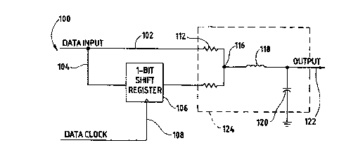
Turning; to Figs. 8 and 9A-9G, a first embodiment of the present invention is
described and iiliustrated. Fig. 8 illustrates a pulse shaping circuit
(generally denoted
by the reference numeral 100). The pulse shaping circuit includes an input
lead 102
which receives a stream ~of data bits that, for example, carry information
using a binary
NRZ data format (although multiple level signals having more than two states
may also
be applied). A tap line 104 connects the input lead 102 with a delay circuit
106. The
signals of both the delay circuit 106 and the input lead 102 are provided
(either directly
or through one; or more; buffers) to a ringing filter circuit 124 that is
specifically
designed to have a ringing characteristic with a predetermined ringing period.
The
ringing period of the ringing filter circuit 124 is selected to be less than
or about equal
to two symbol periods of the data stream provided at the data input of the
circuit 100.
Preferably, the :ringing period is equal to about two symbol periods. In some
instances,
it may be desirable to ;>elect the ringing period to be about one symbol
period in
duration.
By way of example only, the delay circuit 106 may represent a one bit shift
register which shifts data pulses therethrough based on a data clock signal
applied upon
CA 02284695 1999-09-23
WO 98/43358 PCT/US98/05583
-12-
line 108. The delay circuit 106 receives and stores each data bit entered upon
the input
lead 102 for a predetermined propagation delay. The propagation delay of the
delay
circuit 106 is preferably about equal to half of the ringing period of the
ringing filter
circuit. In an even more preferable embodiment, the propagation delay is equal
to about
one symbol period. The delay module 106 outputs a stream of delayed data
symbols
upon line 110. In the illustrated embodiment, the clock signal supplied to the
shift
register would have a clock period equal to the propagation delay. If an N-bit
shift
register were used, the clock signal would have a period equal to the
propagation delay
divided by N.
Fig. 9A illustrates an exemplary stream of data symbols 101 labeled as symbols
A through D. An exemplary delayed data stream 103 is illustrated in Fig. 9B,
in which
each data symbol (A'-D') follows a corresponding data symbol (A-D) in the
original
input data stream 101 by a time T equal to the propagation delay. The original
and
delayed data streams are supplied to the ringing filter circuit 124. More
particularly, in
the present embodiment, the original and delayed symbol streams are supplied
through
resistors 112 and 114 to a common node 116 and to an inductor 118 and
capacitor 120
that are arranged in a low-pass co~guration. The resistors 112 and 114, the
inductor
118 and the capacitor 120 cooperate to define the ringing filter circuit 124
that
combines the symbol streams received upon lines 102 and 110 to produce a
converted
output data stream at line 122.
With reference again to the principles described in connection with Figs. 4 -
8,
the response of the ringing filter can be understood. To this end, the
individual
CA 02284695 1999-09-23
WO 98/43358 PCT/US98/05583
-13-
responses of the ringing filter circuit 124 to pulses A - D are illustrated in
Figs. 9C -
9F, respectivel;r. These signals are combined in the ringing filter circuit
124 to generate
resultant composite waveform illustrated in Fig. 9G. As illustrated, the
composite
waveform includes transition regions 126, 128, 130, 132 and the like, which
have a
substantially sinusoidal shape. As such, the resulting waveform has a
substantially
reduced bandwidth when compared to the bandwidth of the input data stream of
Fig.
9A. Additionalliy, the resulting waveform has no intersymbol interference
associated
with it. Preferably, the re;suiting waveform is acquired at times
corresponding to t, , t2 ,
t, , etc. by any rf;ceiver to which the data is supplied.
Figs. 10, 11A and 11B illustrate an alternative embodiment of the present
invention. In the embodiment of Fig. 10, the shaping and filtering circuit has
been
modified for use in a trmsmission system which supports a mufti-level data
signal
output stream having more than two potential logic levels. In the embodiment
of Fig.
10, four logical levels are; available through the use of two main input leads
150 and
152, each of which may receive a stream of binary data symbols 153 and 155
(although
the input data stream ma.y itself be a multilevel, non-binary stream). The
symbols
within the data streams 153 and 155 are aligned in time to define one of four
logic
levels. For example, when leads 150 and 152 both receive 0-state bits, they
define a
logic level zero.. When leads 150 and 152 receive a 0-state bit and a 1-state
bit,
respectively, they define a logic level one. When leads 150 and 152 receive a
1-state
bit and a 0-state bit, they define a logic level two, and when leads 150 and
152 both
receive 1-state bits, they define a logic level three. The data streams 153
and 155 are
CA 02284695 1999-09-23
WO 98/43358 PCT/US98/05583
-14-
passed through buffers 154 and 156 to a ringing filter circuit 157 which may
include
resistors 158, 160, 162 and 164, inductor 166 and capacitor 168. The ringing
filter
circuit 157 has a ringing period such as described above.
The input leads 150 and 152 are connected at nodes 170 and 172 with tap lines
I?4 and 176 to deliver the incoming streams of data symbols 153 and 155 to a
delay
module 178. The delay module 178 outputs data bit values upon leads 180 and
182
which are received upon incoming tap lines 174 and 176, respectively, after a
predefined delay (such as explained above in connection with the embodiment of
Fig.
8). The delayed data bit streams are passed along lines 180 and 182 through
buffers
184 and 186 to the ringing filter circuit 157 via resistors 162 and 164. By
way of
example only, the delay module may include two one-bit shift registers aligned
in
parallel to receive separately data symbols incoming from lines 174 and 176
and output
same in parallel to lines 180 and 182. Other configurations are likewise
suitable, such
as described above.
The values of resistors 158, 160, 162 and I64 may be defined in a
predetermined relationship to one another. Optionally, resistors 158 and 162
may be
defined as a function of resistors 160 and 164, respectively. By way of
example only,
resistor 158 may equal 1/2 the value of resistor 160, while resistor 162 may
equal 1/2
the value of resistor 164. Resistors 158 and 160 may be set with respect to
resistors
162 and 164, to minimize ripple errors.
Turning to F igs. 11 A and 11 B, Fig. 11 A illustrates an exemplary digital
signal
defined by the binary data bit streams 153 and 155. The digital signal of Fig.
I lA
CA 02284695 1999-09-23
WO 98/43358 PCT/US98/05583
-15-
includes four discrete logic levels 202, 204, 206 and 208, each of which is
defined by a
unique bit combination received upon the leads 150 and 152. In Fig. 10, as
data bit
values are supplied via leads 150, 152, 180 and 182 to the ringing filter
circuit 157,
each data pulse introduces a corresponding component waveform response into
the
resultant signal on output lead 169. Resistors 158, 160, 162 and 164 are
assigned
values as explained above in order to ensure proper attention therebetween of
the
associated component waveform responses. It will be recognized that the logic
levels
need not be equally spaced.
The ringing filter circuit 157 outputs a resultant or composite signal on line
169
(Fig. 10) which resembles the signal illustrated in Fig. 11B in response to
the signal
illustrated in Fig. 11 A. Within the resultant signal 220, transition regions
between
logic levels are shaped to be substantially sinusoidal (see transition regions
222, 224,
226 and the lik:e).
In the foregoing embodiments, the transition regions between logic levels may
occupy a complete clock cycle corresponding to the width of a data bit pulse.
However, the transitions need not be so slow. Instead, the propagation of the
delay
module may be adjusted. in order that the transitions occur in a shorter
period of time in
which case the transitions may be less smooth.
Fig. 1f. illustrates a system in which the foregoing pulse shaping circuits
may
be used. More particularly, the system, shown generally at 300, is basic RF
digital
communications system comprising a transmitter 30~ and receiver 310 that
respectively transmit and receive data over a transmission medium 315, such as
air,
CA 02284695 1999-09-23
WO 98/43358 PCT/EJS98/05583
-16-
cable, etc.. The pulse shaping circuits described herein may be incorporated
in the
baseband filter 320 of the receiver 310.
While particular elements, embodiments and applications of the present
invention have been shown and described, it will be understood, of course,
that the
invention is not limited thereto since modifications may be made by those
skilled in the
art, particularly in light of the foregoing teachings. It is therefore
contemplated by the
appended claims to cover such modifications as incorporate those features
which come
within the spirit and scope of the invention.