Note : Les descriptions sont présentées dans la langue officielle dans laquelle elles ont été soumises.
CA 02299044 2000-02-21
2
COPYRIGHT NOTICE
A portion of the disclosure of this patent document contains material which is
subject to copyright protection. The copyright owner has no objection to the
facsimile
reproduction by anyone of the patent document or the patent disclosure, as it
appears
in the Patent and Trademark Office patent file or records, but otherwise
reserves all
copyright rights whatsoever.
FIELD OF THE INVENTION
This present invention generally relates to meters and monitors of the type
that
measure power consumption and/or power quality. More specifically, the present
invention relates to an automatic gain switching of such meters and monitors.
BACKGROUND OF THE INVENTION
In a typical electrical distribution system, electrical energy is generated by
an
electrical supplier or utility company and distributed to consumers ma a power
distribution network. The power distribution network is the network of
electrical
distribution wires which link the electrical supplier to its consumers.
Typically,
electricity from a utility is fed from a primary substation over a
distribution cable to
several local substations. At the local substations, the supply is transformed
by
distribution transformers from a relatively high voltage on the distributor
cable to a
lower voltage which is supplied to the end consumer. From the substations, the
power
is provided to industrial users over a distributed power network that supplies
power to
various loads. Such loads may include, for example, various power machines
used by
the end consumer.
At the consumer's facility, there will typically be a meter connected between
the consumer and the power distribution network to measure the consumer's
power
consumption and/or power quality. The revenue meter is an electrical energy
measurement device which accurately measures the amount of electrical energy
flowing to the consumer from the supplier. The amount of electrical energy
measured
by the meter is then used to determine the amount for which the energy
supplier
should be compensated.
CA 02299044 2000-02-21
3
Typically, the electrical energy is delivered to the consumers as an
alternating
current (AC) voltage that approximates a sine wave over a time period. The
term
alternating waveform generally describes any symmetrical waveform, including
square, sawtooth, triangular, and sinusoidal waves, whose polarity varies
regularly
with time. The term AC (i.e., alternating current), however, almost always
means that
the current is produced from the application of a sinusoidal voltage, i.e., AC
voltage.
The expected frequency of the AC voltage, e.g., 50 Hertz (Hz), 60 Hz, or 400
Hz, is
usually referred to as the fundamental frequency. Integer multiples of this
fundamental frequency are often referred to as harmonic frequencies.
While the fundamental frequency is the frequency that the electrical energy is
expected to arrive with, various distribution system and environmental factors
can
distort the fundamental frequency, i.e., harmonic distortion, can cause
spikes, surges,
or sags, and can cause blackouts, brownouts, or other distribution system
power
quality problems. These problems can greatly affect the quality of power
received by
the power consumer at its facility or residence as well as make difficult an
accurate
determination of the actual energy delivered to the consumer.
In order to solve these problems, revenue meters have been developed to
provide improved techniques for accurately measuring the amount of power used
by
the consumer so that the consumer is charged an appropriate amount and the
utility
company receives appropriate compensation for the power delivered and used by
the
consumer. Examples of such metering systems are well known in the art.
In addition, power monitors, and revenue meters with power monitoring
capabilities, provide information about the quality of the power, i.e.,
frequency and
duration of blackouts, brownouts, harmonic distortions, surges, sags, swells,
imbalances, buntings, chronic overvoltages, spikes, transients, line noise, or
the like,
received by a power consumer at a particular consumer site. Blackouts,
brownouts,
harmonic distortions, surges, sags, swells, imbalances, buntings, chronic
overvoltages,
spikes, transients and line noise are all examples of power quality events. As
utility
companies become more and more deregulated, these companies will likely be
competing more aggressively for various consumers, particularly heavy power
users,
and the quality of the power received by the power consumer is likely to be
important.
CA 02299044 2000-02-21
4
This, in turn, means that accurate and detailed reporting and quantification
of power
quality events and overall power quality will become more and more important
as
well.
For example, one competitive advantage that some utility companies may have
over their competitors could be a higher quality of the power supplied to and
received
by the consumer during certain time periods. One company may promote that it
has
fewer times during a month that power surges reached the consumer causing
potential
damage to computer systems or the like at the consumer site. Another company
may
state that it has fewer times during a month when the voltage level delivered
to the
consumer was not within predetermined ranges which may be detrimental to
electromagnetic devices such as motors or relays. Previous revenue accuracy
meters
which provide for measuring quality of power in general lack the necessary
accuracy
and power quality monitoring features to provide the consumer and the power
utility
with the needed inforniation.
Problems occur since power monitors often are called upon to cover a wide
range of voltage and current, such as 0 to 1000 Volts (V) Root Mean Square
(RMS)
and 0 to SO Amps (A) RMS. To handle the wide range of voltage and current, one
known solution is to include a mechanical or electronic switch that
interchanges
between different voltage and current ranges of the meter. Such switching is
commonly referred to as gain switching. For example, if an input voltage
exceeds the
meter setting, the switch is changed to a different gain setting. The
mechanical or
electronic switching of the power monitor, however, may cause samples to be
missed
since no samples above the range are accurately recorded until the power
monitor is
switched.
Another known solution used to accommodate a wide range of input voltage
and current is to utilize an Analog to Digital Converters (ADC) having a high
bit
count that handles a wide range of voltage and current. While power monitors
commonly use an ADC with a bit count of 12 bits or less, ADCs with a bit count
of 1 G
bits or higher are available. The 16 bit or higher ADCs, however, are
prohibitively
expensive in today's market. In addition, the overall system design becomes
more
complex and more costly due to signal/noise and data processing issues. At the
CA 02299044 2000-02-21
bottom end of the bit range, a signal/noise ratio decreases, especially in
industrial
applications, to produce poor quality signals. The best resolution occurs at
the top end
of the ADC's bit range, e.g., 10 to 12 bits for a 12 bit ADC. High resolution
and
accuracy are especially important, for example, in applications such as a
waveform
5 recorder of the power monitor which allows a user to view line conditions in
oscilloscope like form.
To obtain accurate readings, other known techniques include producing
customized devices that accommodate a predetermined input range of voltage and
current specified by the consumer. The customized power monitors contain
amplifiers, for example, that provide gain to the signal to place the signal
at the high
bit range of the ADC 18. During the production process the amplifier circuit
is
adjusted to provide the required gain. It can be appreciated, however, that
such
customized devices increase manufacturing costs and complicate production
procedures and logistics. In addition, the customized meters do not address
problems
caused by transients, such as voltage spikes and swells, that can exceed the
normal
operating conditions of the meter by several hundred percent. Thus, a voltage
spike
of, e.g., 1000 V RMS can saturate the ADC 18 to its maximum bit count which
indicates, e.g., only 120 V RMS. Such saturation of the ADC 18 creates a
clipped
sample of the signal.
Accordingly, there is a need for a power monitor that is capable of
monitoring,
reporting and quantifying the quality of power with high level of detail and
accuracy.
Further, there is a need for a power monitor that guarantees no missing or
clipped
samples within a wide operating range of input voltages and currents. In
addition,
there is a need for a power monitor that eliminates production difficulties
and costs
associated with customized power monitors.
SUMMARY OF THE INVENTION
Such needs are met or exceeded by the present method and device for
automatic control of gain switching. In general, device and method for gain
switching
improves power monitor and/or revenue meter operation within a wide range of
input
voltages and currents. Further, firmware controlled gain switching allows the
power
Image
CA 02299044 2003-07-25
I~~~F'~ #,.s~::,~'','3~..~~'~~s~3~ ~.r#"" ~~~"~~:: ~_~#~'~.,~-~t~a~zff~'~ ~ i
'....~"3.F 1>:st ~~5.'S.~~~~~.~''Y ~~c'~S~~ ~1~~~>~4~~~'S ~~ ~~ f2 t;1 M'~f
:CSfJ7 5 yf~#~~ ~ 4~~#~~~~~~~~ ~~'~ G~~~ 2~
e;~~~~r~~:
=~ ~°!~~~#~'~ "~ ;~~;y3~~'~~ c'~
~~~i~rr;~C~si~~t'c'~~~''~~~~f~~,t~?'~z,'~,r3~~3~~t~~~ts'.~i'a,
~~~33~~~f~'~;;;«'~~~~#~ ~~'~:~
1'W3~.''s''~#"#~'4 s~'#.'~'.si't'~'r~r%~~~; 4~'~ ~i?~:' ~~i#"~~~f.~3~~'~t',~t,
'~%'~~#~3~,~~~'s~'s~3<3<'?'.'~ ~"~'~x~'~;t" f'~'3f3''s#a~,~3'.
~#''vf'.~~=~"s.~. ~ a~~~F;,~ ~t:~~~c~t3~ iCls.'3~'~ ~'~'~i.##''s:'3~;f~
~~'~~f~~t~ls's~~°Q .'~.~'~'F~?'C'~'~~~~ s~t~f~~ c.~>.#i'~
~;:~~'#:~~Y?M"~~
;''°~; " '~'' ~';''ei~°~~' s'~tis"~ a'1~~~(.:~'i#t~~~~
~iw'~sqi'r:?~' ~~LSt~''s~~~ii~' E3s~ ~~~% f"'.ti'~~~a'~'~
1~"'t;d~'.#~'~~'~.'~"3~'s;
ife Gc~t,..,.'t e,"..
~v~t;~F'~ ~ ~~'r~..~7#~,~ x ~Xt~~'~i~ x~~~~~ ~1'~~.~L~~ ~;s,~YY~':~'~'~
~~~~'~~~ ~~#" ~~"!3.~~1.~~ ~~la"r ~:~:c~~#'f~~
~tf~~'F~4':"i ~~"? ~~'~,'~,#~~~.~'.3 ,~f
CA 02299044 2000-02-21
Figure 5 shows a flow chart depicting a voltage channel gain control algorithm
of the present automatically controlled gain switching power monitor;
Figure 6 shows a flow chart depicting a current channel gain control algorithm
of the present automatically controlled gain switching power monitor;
Figure 7 depicts a perspective view of an exemplary S-Base revenue meter and
socket type detachable meter mounting device for connecting the meter to an
electrical circuit, for use with the present automatic gain control algorithm;
Figure 8 shows the blade type terminals on the back of the revenue meter
depicted in Figure 7;
Figure 9 shows exemplary layouts of the matching jaws of the detachable
meter mounting device of Figure 7 for receiving the blade type terminals shown
in
Figure 8;
Figure 10 depicts a perspective view of an exemplary A-Base revenue meter
with bottom connected terminals for connecting the meter to an electrical
circuit, for
use with the present automatic gain control algorithm;
Figure 11 depicts a perspective view of an exemplary switchboard revenue
meter and meter cover, for use with the present automatic gain control
algorithm; and
Figure 12 depicts a perspective view of the exemplary switchboard revenue
meter of Figure 1 l, with the draw-out chassis, which holds the meter
electronics,
removed.
TABLE OF ACRONYMS
The following table aids the reader in determining the meaning of the several
acronyms used to describe the present invention:
A = Amps.
AC = Alternating Current.
ADC Analog to Digital
= Converter.
CPU Central Processing
= Unit.
CTR Cun ent transducer.
=
DMA = Direct Memory Access.
DSP = Digital Signal Processor.
CA 02299044 2000-02-21
$
Hz = Hertz.
PTR = Potential or voltage transducer.
RMS = Root Mean Square.
V = Volts.
DETAILED DESCRIPTION OF THE INVENTION
The automatic controlled gain switching of the present invention is used by
power monitoring devices and revenue meters, herein referred to as monitors.
Automatic controlled gain switching improves accuracy and waveform recording
quality compared to monitors that fails to use gain switching. In addition,
the
automatic controlled gain switching allows the monitor to record voltage and
current
transients of magnitudes exceeding normal power system operating conditions by
several hundred percent. The gain switching of the present invention
guarantees no
missing or clipped samples in the waveform recordings and calculations.
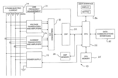
Referring to the drawings, and particularly Figure 1, a monitor, generally
indicated as 10, contains hardware components which can detect and report
power
quality events. Logically, the preferred monitor 10 is comprised of hardware,
software, and firmware. Figure 1 shows a typical hardware configuration where
the
monitor 10 is connected to a power supply 12 and a three phase electric
circuit 14. It
will be appreciated by those skilled in the art that the algorithms detailed
herein can
be executed by a variety of hardware configurations, all of which are known in
the art.
The power supply 12 of the preferred embodiment includes a very wide operating
range true three phase power supply. This permits the monitor 10 to operate
with
different input voltage conditions without necessitating different hardware,
which
permits a utility to stock fewer monitor types in their inventory. The power
supply 12
supplies power for the meter's electronics.
Exemplary voltage inputs include three phase 120-277 V RMS +/s 20% (for a
4 wire Wye 9S connection) or 120-4$0 V RMS (for a 3 wire Delta SS connection).
Wye is a defined wiring system for three phase power where four power carrying
conductors are used, one of which is a neutral conductor. Delta is a defined
wiring
system for three phase power utilizing three power carrying conductors. Either
wiring
CA 02299044 2000-02-21
9
system can include an extra safety ground conductor. Continuing with the power
supply 12, multiphase operation also effectively reduces the power consumption
of
the monitor 10 by equally dividing monitor power requirements between each
phase.
In addition, true three phase operation provides the ability for the monitor
10 to
continue normal operation with two out of three input phase loss (single phase
operation) in a four wire Wye configuration and the loss of a single phase in
a three
wire delta configuration.
Referring also to Figure 2, the monitor 10 contains transducers 16, including
current transducers (CTR) and potential or voltage transducers (PTR) which
sense
current channels I,, Iz, and I3, and voltage channels Va, Vb, and Vc
respectively,
corresponding to each phase of the three phase input. In addition, auxiliary
voltage V4
and currents I4 and IS are input to the monitor to measure, for example, a
neutral
current, a ground current and a star point voltage in a three phase WYE
system,
respectively. Monitors equipped with the fourth current can directly measure,
with
I 5 high precision, the magnitude of the neutral or ground current. The
ability to directly
measure neutral or ground current ensures that the power system operates
within safe
limits. In addition, the fourth voltage and the fifth current can be used to
monitor
other current or voltage signals, e.g., corresponding to a load, auxiliary
transducer
output or other diagnostic measurement points in a system.
Referring to Figures 2 and 3, the three phase voltage input channels Va, Vb,
and Vc are internally split into two gain channels each, herein referred to as
a nominal
gain channel and an overrange gain channel. A two stage amplifier (not shown),
for
example, connects to the voltage channels to scale the input voltage and
provide for
different gain channels. An exemplary input peak voltage versus an Analog to
Digital
Converter (ADC) count is shown for the different gain channels. For the sake
of
simplicity, the absolute values are shown for the peak input voltages and the
ADC
counts. Thus, it can be appreciated that Figure 3 also is applicable for the
negative
peak input voltages and ADC counts.
For a I 2 bit ADC, an absolute value of the ADC count ranges from 0 to 4096.
In the preferred embodiment, the nominal gain channel covers a voltage range
of
about 0 to 15G V RMS (221 V peak), and the overrange gain channel encompasses
a
CA 02299044 2000-02-21
range of about 0 to 1000 V RMS (1414 V peak) or greater. Artisans will
appreciate
that these voltage ranges and channels are implementation dependent and can be
changed for other applications. In addition, it should be appreciated that
switch points
can vary from unit to unit due to tolerances in the electronic circuitry.
These
variations, however, do not adversely effect the overall gain switching of the
present
invention.
Note, as used herein, that the term ADC converter refers not only to a
traditional A/D converters but also to a Time Division Multiplication ("TDM")
based
converter, or other converter which converts analog signals to digital
signals. TDM is
10 a method of measuring instantaneous power over a wide range of input
voltages.
TDM is accomplished by taking a snapshot of the waveform of the incoming
electrical signal and converting it to a square wave over time using a known
algorithm. The area of this square wave is then proportional to the power at
the time
the snapshot was acquired. The snapshot or sample time is dependent on
processor
speed. An exemplary implementation of TDM is the Quad4-Plus Electric Meter
manufactured by Process Systems, A division of Siemens Power and Transmission
&
Distribution, LLC, located in Raleigh, North Carolina which is described in
the CD
ROM specification for this product.
Referring to Figures 2 and 4, the three phase current input channels I~, IZ,
and
I3 are internally split into four gain channels and scaled using four
amplifiers
connected in parallel, for example. Exemplary current gain channels are a
creep gain
channel, an underrange gain channel, a nominal range channel and an overrange
gain
channel. In addition, I4 and IS are internally split and scaled into the
underrange and
overrange gain channels. Two gain channels, instead of four, are preferred for
I4 and
IS to reduce costs by using only two gains since a highly accurate measurement
of I4
and I5 are not required. An exemplary input peak current versus ADC count is
shown
in Figure 4 for the different gain channels. For the 12 bit ADC, an absolute
value of
the ADC count ranges from 0 to 4096. In the preferred embodiment, the creep
gain
channel covers a current range of about 0 to .8 A RMS ( 1.13 A peak), the
underrange
gain channel encompasses about 0 to 3.125 A RMS (4.4 A peak), the nominal gain
channel is about 0 to 12.5 A RMS (17.7 A peak), and the overrange gain channel
CA 02299044 2000-02-21
11
covers a current range of about 0 to 50 A RMS (70.7 A peak). Artisans will
appreciate that these current ranges and channels are implementation dependent
and
that other current ranges are possible. In addition, it should be appreciated
that switch
points can vary from unit to unit due to tolerances in the electronic
circuitry. These
variations, however, do not adversely effect the overall gain switching of the
present
invention.
Referring also to Figure 1, the transducers 16 permanently connect, i.e.,
without mechanical switching, each gain channel signal to at least one ADC 18.
The
ADC samples the analog current and voltage in each phase for each gain channel
of
the electric circuit 14, and converts the analog signal to a digital signal
for each gain
channel. Thus, information is gathered for all gain channel signals at all
times, even if
the gain channel signal is saturated, to guarantee no missing or clipped
samples.
In a preferred embodiment, the gain channel signals connect to an array of
three ADCs 18 of the "12 bit plus sign" type with a count range from -4096 to
4096.
Each ADC 18 samples up to eight channels simultaneously, where simultaneously
is
defined herein as within one hundred microseconds. Thus, a total of twenty
four
channels are sampled simultaneously. Preferably, at least one voltage gain
channel
and one current gain channel representing the same phase of the power system
may be
sampled simultaneously to preserve the phase relationship between the voltage
and
the current signals. When voltage and current are not measured simultaneously,
the
phase relationship of voltage and current signals is not preserved, which
adversely
affects the calculation of power and energy. Correction of phase errors
induced by the
sampling sequence is effective only when operating at the fundamental
frequency.
More preferably, all of the gain channels are sampled simultaneously.
Data from all of the sampled gain channels are stored to memory, whether or
not the sample is saturated, as further described below. During half cycle
task
calculations, described below, a running average is calculated for unsaturated
channels of the stored samples. Thereafter, during one second task
calculations,
described below, a weighted running average is calculated for the unsaturated
channels.
CA 02299044 2003-O1-13
12
During sampling, a Digital Signal Processor (DSP) 20 utilizes a sampling
algorithm to control the array of the three simultaneously operating ADCs 18.
An
exemplary DSP is the TMS 320C203 manufactured by Texas Instruments, Inc.,
located in Dallas, Texas. The line fi-equcncy, c.g., 60 1-lcrtz (1-1Z), is
measured (block
21) and utilized by the CPU which calculates the sampling interval and
transfers it via
Direct Memory Access (DMA) to the DSP. The DMA method is described in a
commonly assigned co=pending patent application to Rene T. Jon~or, et al.
entitled
"Revenue Meter with Power Quality Features," patent No. 6;493,644, issued
December 10, 2002.
DMA transfer is preferred since such a transfer
IO requires minimal external hardware to operate. Thus, there is no need for
use of
costly dual port memories, which results in significant cost savings. The DMA
method also provides a higher overall data throughput with less CPU loading.
Alternatively, other methods of sharing data between the CPU 22 and DSP 20 can
also be used. In a preferred embodiment, the DSP 20 samples the voltage at a
rate of
128 samples per cycle for riput signal frequencies of 18 Hz to 72 Hz to
achieve, e.g.,
a resolution of 434 micro-~econd for 18 Hz 156 micro-second for SO Hz 130
micro-
second resolution at GO Hz, and 108 micro-second for 72 Hz. Generally
resolution =
[I/(input frequency* 128)].
In addition, artisans will appreciate that sampling rates as low as 16 samples
per cycle can be used, and that higher sampling rates such as 256 samples per
cycle
can also be used. The maximum sampling rate is limited by a processing power,
an
analog to digital converting speed limit of the ADC, and cost. Since more
samples
per cycle produce more information to allow better reconstruction of the
signal, the
minimum sampling rate is governed by a required accuracy of the monitor 10. It
is
found that 128 samples of each gain channel per cycle achieves the required
accuracy
and provides the best cost per performance ratio in today's market.
The ADC I8 outputs the samples for each gain channel to the DSP 20. The
DSP 20 soras the samples by gain channel, loads the sorted samples into
corresponding sample buffers, and also sends the samples to a Central
Processing Unit
(CPU) 22 for further processing, described below. A preferable method for
sending
CA 02299044 2000-02-21
13
the samples to the CPU is via DMA. The CPU 22 manages and stores results for
later
user access.
The DMA data transfer uses the passive DMA capabilities of the DSP 20 and
DMA controller functionality provided by the CPU 22. As described above, the
DSP
20 executes the sampling algorithm and collects samples. The samples are
sorted by
channel and stored in sample buffers located in a designated SRAM memory 24.
Each gain channel is associated with its own sample buffer that is at least
five half
cycles long. The buffer is deep enough so that the CPU 22 can access samples
from
the buffers after performing pre-calculations described below. In the
preferred
embodiment, six half cycle buffers are used for ease of implementation. In
addition to
these sample buffers, there are at least two pre-calculation buffers allocated
for
transferring pre-processed data between the CPU 22 and the DSP 20. An
identical
buffer arrangement exists in the CPU's DRAM memory 25.
Utilizing sample data stored in the sample buffers, the DSP 20 executes gain
control of the present invention to provide for automatically controlled gain
switching.
Preferably, the present gain control algorithm is executed with firmware that
resides
in flash memory on the CPU 22 when the DSP 20 is powered down, and which is
automatically downloaded into DSP operation memory when the monitor is powered
up. Artisans will appreciate, however, that the present gain control algorithm
can be
implemented in other ways, for example, by using hardware or software.
Referring to Figures 5 and 6, the flowcharts represent the gain control
algorithm of the present invention. In general, the DSP 20 scans all gain
channels,
sample by sample, to eliminate saturated channels. Moreover, the DSP 20
selects
optimal gain channels, i.e., those that provide the best utilization of the
ADC input
voltage range for the present magnitude of signals. For example, for a twelve
bit
ADC, with a 0 to 5 input voltage, i.e., producing up to 4096 counts, the
desired input
signal level is as close to 5 V as possible. Signal levels of SV or more
result in ADC
saturation at 4096 counts. Gain selection information is stored in an internal
data
structure on the DSP 20, for example, to signify the channels with the best
ADC
resolution for a predetermined time interval.
CA 02299044 2000-02-21
14
Referring to Figure 5, a flowchart is shown that represents voltage gain
control
for the nominal and overrange voltage gain channels. The present gain control
algorithm utilizes a one cycle wide sliding window to view samples from the
three
cycle wide sample buffers. While the sliding window is one cycle wide, it only
advances in one-half cycle increments. Thus, when the sliding window advances,
it
covers a previous one-half cycle of samples and a present one-half cycle.
Advancing
the window one-half cycle at a time lends for a more stable output, e.g., by
eliminating bounce and discontinuities, than if the window moved one cycle at
a time.
Further, the sliding window arrangement improves a response time of the meter
since
the gain control information is updated every one-half cycle instead of every
cycle.
Thus, the gain control algorithm begins by shifting the sliding window one
half
cycle (block 25) to access the present voltage nominal samples and voltage
overrange
samples, for each voltage phase Va, Vb, and Vc (block 26). Thereafter, the DSP
20
determines whether any of the samples within the present one-half cycle are
saturated
in the Va nominal buffer (block 28). For a 12 bit ADC, a sample is saturated
when
the sample shows an ADC count of 4096. In the preferred embodiment, a sample
is
considered to be saturated when the sample manifests an ADC count of 4090 to
4096.
Artisans will appreciate, however, that other counts can be used as a
saturation level
for the purpose of the present invention. If any samples are saturated, the
DSP 20 sets
the gain selection information to select the samples from the overrange sample
buffer
within the one cycle window for Va, Vb, and Vc (block 30).
In addition, the DSP 20 sets a previous-gain-stage indicator for each gain
channel of this half cycle. During the next one-half cycle, the previous-gain-
stage
indicator represents the optimal range of this half cycle, which will then be
the
previous one-half cycle. As evidenced below, the DSP 20 checks the previous-
gain-
stage indicator to acquire optimal range information for the previous one-half
cycle
without rechecking all the samples in that cycle. In this manner, the previous-
gain-
stage indicator optimizes time and saves processing power.
If no samples are saturated within the present one-half cycle for the Va
nominal sample buffer, the DSP 20 sets the previous-gain-stage indicator to
nominal
for channel Va (block 31). Thereafter, the DSP 20 determines whether any
samples
CA 02299044 2000-02-21
are saturated in the present one-half cycle Vb nominal buffers (block 32). If
the Vb
nominal buffer contains at least one saturated sample in the present nominal
buffer,
the DSP 20 selects the samples within the one cycle window for the overrange
buffers
of Va, Vb, and Vc (block 30). In addition, the DSP 20 sets the previous-gain-
stage
5 indicator to overrange (block 30). Otherwise, the DSP sets the previous-gain-
stage
indicator to nominal for channel Vb (block 33).
If no samples are saturated within the present one-half cycle for each of the
Va,
Vb, and Vc nominal buffers, then the DSP 20 sets the previous-gain-stage
indicator to
nominal for Vc (block 35). Thereafter, the DSP 20 determines whether the
nominal
10 gain channel was selected in the previous half cycle. To determine whether
the
nominal gain channel was selected, the DSP 20 checks a value of the previous-
gain-
stage indicator for the previous one-half cycle. If the previous-gain-stage
indicator
indicates the nominal range for each of Va, Vb, and Vc during the previous one-
half
cycle (blocks 3G, 38, and 40), then the DSP 20 selects the samples within the
one
15 cycle window for the nominal buffers of Va, Vb, and Vc (block 42).
Otherwise, if any of the previous-gain-stage variables for Va, Vb, and Vc
indicate that the nonunal range was not selected in the previous one-half
cycle (blocks
36, 38, and 40), then the DSP 20 selects the samples within the one cycle
window for
the overrange buffers of Va, Vb, and Vc (block 30). Thus, the DSP 20 selects
Va, Vb,
and Vc in the same gain range to facilitate the calculation of line to line
voltages since
less processing power is required to calculate the vector products when the
gains exist
in the same range. Artisans will appreciate, however, that it is possible to
calculate
line-to-line voltage without the same gain stage requirement.
In addition, the DSP 20 determines a gain range for voltage V4 independent of
Va, Vb, and Vc. After the DSP 20 selects the optimal gain channel for Va, Vb,
and
Vc, the DSP 20 determines whether any of the samples within the present one-
half
cycle are saturated in the V4 nominal buffer (block 44). If any samples are
saturated,
the DSP 20 sets the gain selection information to select the samples from the
overrange sample buffer within the one cycle window for V4 (block 46).
Moreover,
the DSP 20 sets the previous-gain-stage indicator for V4 to overrange.
CA 02299044 2000-02-21
16
If no samples are saturated within the present one-half cycle V4 nominal
buffer, then the gain selection algorithm determines whether the DSP 20
selected the
nominal gain channel for V4 in the previous one-half cycle (block 48), as
discussed
above. If the DSP 20 selected the nominal range in the previous one-half
cycle, then
the DSP 20 selects the samples within the one cycle window for the nominal
buffers
of V4 (block 50). Otherwise, the DSP 20 selects the samples within the one
cycle
window for the overrange buffers of V4 (block 46) Thereafter, the DSP 20 saves
the
gain selection information for Va, Vb, Vc, and V4 to the DSP 20, for example,
and the
necessary data pointers (block 52). The saved information represents the
optimal gain
1 b for the present one-half cycle and the optimal gain for the combination of
the previous
and present one-half cycles to be used in calculation tasks described below.
Similar to voltage V4, the DSP 20 independently determines the optimal range
for currents, such as I,, Iz, I3, I4 and L5, because having varying gain
stages for each
current results in more accurate measurements. Referring to Figure 6, a flow
chart
represents the gain control algorithm for automatically selecting the optimal
current
gain channel for current. The algorithm begins by setting the first current
channel
(block 53) and accessing the latest one-half cycle current sample buffers for
all gain
stages (block 54), starting with current I,, for example. The current channel
selection
portion of the algorithm repeats until the gain channel is determined for each
current
input channel.
Thus, for current I,, the DSP 20 determines whether any samples within the
one-half cycle are saturated for the present creep range buffer (block 56). If
at least
one of the samples is saturated, i.e., the ADC count indicates 4090 or more
counts for
a 12 bit ADC, the DSP 20 determines whether any samples are saturated within
the
current one-half cycle for the present I, underrange buffer (block 58). If at
least one
of the samples is saturated in this range, the DSP 20 determines whether any
of the
samples are saturated in the present nominal range buffer (block 60). If at
least one of
the samples is saturated, the DSP 20 selects the samples within the one cycle
window
for the oven-ange buffer of I, and sets the previous-gain-stage indicator to
overrange
(block 62). In addition, a present-gain-stage indicator is set to overrange
(block 63).
Thereafter, the DSP 20 saves the gain selection information and the necessary
data
CA 02299044 2000-02-21
17
pointers (block 64). The optimal gain for the present one-half cycle and the
optimal
gain for the combination of the previous and present one-half cycles are used
in
calculations described below.
If none of the samples are saturated in the present creep range buffer (block
56), the DSP 20 sets the previous-gain-stage indicator to creep (block 67),
and
determines whether the creep range was selected in the previous buffer (block
68). To
determine whether creep was selected in the previous buffer, the DSP 20 checks
a
value of the previous-gain-stage indicator of I, for the previous one-half
cycle. If the
creep range was selected in the previous buffer, the DSP 20 selects the
samples within
the one cycle window for the creep buffer (block 70). Otherwise the DSP 20
determines whether the underrange was selected in the previous buffer (block
72). If
the undel-range was selected in the previous buffer, the DSP 20 selects the
samples
within the one cycle window for the underrange buffer (block 74). If not, the
DSP 20
determines whether the nominal range was selected in the previous buffer
(block 76).
If the nominal range was selected in the previous buffer, the DSP 20 selects
the
samples within the one cycle window for the nominal buffer (block 78).
Otherwise,
the DSP 20 selects the samples within the one cycle window for the overrange
buffer
(block 63). In this manner, the DSP 20 determines the optimal range for
current I,,
i.e., the range that produces the highest analog to digital count without
containing any
saturated samples.
If samples are saturated in the present creep range but not in the present
underrange range (blocks 56 and 58), the DSP 20 sets the previous-gain-stage
indicator to underrange for I, (block 79). In addition, the DSP 20 determines
whether
the creep range (block 80) or the underrange range (block 72) were selected in
the
previous buffer by checking a value of the previous-gain-stage indicator for
the
previous one-half cycle. If the creep range or the underrange range were
selected in
the previous buffer, the DSP 20 selects the samples within the one cycle
window for
the underrange buffer (block 74). If not, the DSP 20 determines whether the
nominal
range was selected in the previous buffer by checking a value of the previous-
gain-
stage indicator (block 76). If the nominal range was selected in the previous
buffer,
the DSP 20 selects the samples within the one cycle window for the nominal
buffer
CA 02299044 2000-02-21
18
(block 78). Otherwise, the DSP 20 selects the samples within the one cycle
window
for the overrange buffer (block 63).
Likewise, if samples are saturated in the present creep range and the present
underrange buffer, but not the present nominal range buffer (blocks 56, 58,
and 60),
the DSP 20 sets the previous-gain-stage indicator to nominal for this half
cycle
(block 81 ). In addition, the DSP determines whether the creep range (block
82), the
underrange range (block 84), or the nominal range (block 76) were selected in
the
previous buffer by checking a value of the previous-gain-stage indicator for
the
previous one-half cycle. If any of the creep range, the underrange range, or
the
nominal range were selected in the previous buffer, the DSP 20 selects the
samples
within the one cycle window for the nominal range buffer (block 78).
Otherwise, the
DSP 20 selects the one cycle window for the overrange buffer (block 63). The
DSP 20 save all the gain selection and data pointer information (block 64),
and
continues in this manner to determine the optimal gain channel for each
current
1 S channel until no other current channels remain (block 85a). The current
channels are
processed, one by one, until no more current channels exist for the current
half cycle
(blocks 85a and 85b). Thereafter, the DSP 20 shifts the window one-half cycle
and
the above process is repeated for all of the voltage and the current channels
(block 25).
Referring again to Figure 1, the DSP 20 supplies the results of the gain
selection information and pre-calculation information to the CPU 22 via the
DMA
transfers described above. Pre-calculation information includes, but is not
limited to,
half cycle voltage and current RMS, active, reactive, and apparent power
values. An
exemplary CPU is the Power PC MPC821, manufactured by Motorola, Inc., located
in
Schaumburg, Illinois. The CPU 22 then performs half cycle and one second
tasks,
described below, and supplies the results to the user via a user interface 86.
In a
preferred embodiment, the half cycle task utilizes all the samples stored in
the buffer,
i.e., the samples which represent one half cycle of the input waveform. It
should be
appreciated, however, that the calculations can be performed with a lower
number of
samples, e.g., representing a quarter cycle or an eighth of a cycle, down to a
single
sample. The processing power of the DSP and CPU is a limiting factor. In
addition,
CA 02299044 2000-02-21
1~
the expense of the required hardware should be weighed against the increase in
resolution.
EXPLANATION OF SYMBOLS
N - number of samples per cycle.
V - voltage channel.
I - current channel.
GAIN I - optimal gain of current
channel.
GAIN V - optimal gain of voltage
channel.
GAIN VA - optimal gain of voltage
channel Va.
GAIN VB - optimal gain of voltage
channel Vb.
GAIN VC - optimal gain of voltage channel V c.
GAIN IA - optimal gain of current channel Ia.
GAIN IB - optimal gain of current channel Ib.
GAIN-IC - optimal gain of current channel Ic.
The following information is provided, for example, using lookup
tables.
RMS Scale[any gain] - user configurable scale of voltage or current based on
a current transformer or potential transformer.
Power_Scale[V][I] = RMS Scale[V] * RMS-Scale[I].
Calibration Factor[ any gain ] - factory configured calibration number for
every gain channel.
Power Calibration Factor[ voltage gain] [current gain ] _
RMS Calibration Factor[voltage gain]
RMS Calibration Factor[current gain].
The DSP uses a one cycle calculation window which slides by one half cycle.
The pre-processing of raw (unscaled and uncalibrated) data consists of, but is
not
limited to, the following calculations:
Per channel:
CA 02299044 2000-02-21
Optimal gain, hereafter GAIN, is selected from all sampled gain channels, per
the auto-ranging routine of the present invention.
Sum of all samples in a cycle for the selected optimal gain channels,
hereafter
RAW SUM[GAIN].
5 Sum of all squared samples in a cycle for the selected optimal gain
channels,
hereafter RAW_SSQ[GAIN].
RMS value of all samples in a cycle for the selected optimal gain channels,
hereafter RAW RMS[GAIN].
Peak value of samples in a cycle for the selected optimal gain channels,
10 hereafter RAW PEAK[GAIN].
Per phase of the power system:
(Where voltage V and current I belong to the same phase of the power system).
Product of voltage RAW SUM[GAIN_V] and current RAW_SUM[GAIN_I],
15 hereafter RAW VISUM[GAIN V][GAIN-I];
Sum of products of voltage and current samples for a cycle, hereafter
RAW VIW[GAIN-V][GAIN_I];
N
RAw_mw[GAIN v][GAIN-I] _ ~ fv; * i;~
2o i=o
where:
v; - i-th sample in the optimal gain of voltage GAIN V,
i; - i-th sample in the optimal gain of current GAIN I.
Sum of products of voltage samples displaced by 90 degrees (with respect to
current samples) and current samples for a cycle, hereafter
RAw_vlv[GAIN-v] [GAIN_I];
N-N/4 N/4
CA 02299044 2000-02-21
21
RAW VIV[GAIN V][GAIN I] _ ~ fv~;+Nia) * i;} + ~ fv; * it;+~N-Nia)>]
i=0 i=0
where:
v; - i-th sample in the optimal gain of voltage GAIN-V,
i; - i-th sample in the optimal gain of current GAIN I.
Sum of products of voltage samples displaced by 45 degrees (with respect to
current samples) and current samples for a cycle, hereafter
RAW VIQ[GAIN-V][GAIN-I];
N-N/8 N/8
RAW VIQ[GAIN-V][GAIN-I] _ ~ {v(;+Nis) * 1;] + ~ ]v; * lc;+cN-Nis))]
i=0 i=0
where:
v; - i-th sample in the optimal gain of voltage GAIN V,
i; - i-th sample in the optimal gain of current GAIN I.
Active power for a cycle using RAW VIW[GAIN-V][GAIN I] and
RAW VISUM[GAIN-V][GAIN-I], hereafter RAW W[GAIN V][GAIN-I], where
RAW W [GAIN V] [GAIN-I] = RAw vlw[GAIN-v] [GAIN-I] -
RAW VISUM[GAIN_V][GAIN-I].
Reactive power for a cycle using RAW VIV[GAIN V][GAIN-I] and
RAW VISUM[GAIN V][GAIN-I], hereafter RAW VAR[GAIN-V][GAIN-I],
where RAW VAR[GAIN V][GAIN-I] = RAW VIV[GAIN_V][GAIN I] -
RAW VISUM[GAIN V][GAIN_I].
Additional calculations are performed to support line to line voltage
calculations:
Sum of the products of phase voltage A samples and phase voltage B samples,
hereafter RAW VAB[GAIN_VA][GAIN VB];
CA 02299044 2000-02-21
22
N
RAW VAB[GAIN VA][GAIN VB] _ ~ {va; * vb;}
i=0
where:
va; - i-th sample in the optimal gain of voltage GAIN VA,
vb; - i-th sample in the optimal gain of voltage GAIN VB.
Sum of the product of phase voltage B samples and phase voltage C samples,
hereafter RAW VBC[GAIN VB][GAIN-VC]; calculated using analogous
mathematical operations for RAW VAB described above.
Sum of the products of phase voltage C samples and phase voltage A samples,
hereafter RAW VCA[GAIN-VA][GAIN VC]; calculated using analogous
mathematical operations for RAW VAB described above.
Using phase A voltage and phase B current, and the sum of the product of
voltage and current samples for a cycle, hereafter
RAwyw_AB[GAIN vA][GAIN-IB];
N
RAW VIW AB[GAIN VA][GAIN IB] _ ~ {va; * ib;}
i=0
where:
va; - i-th sample in the optimal gain of voltage GAIN VA,
ib; - i-th sample in the optimal gain of current GAIN-IB.
Using phase A voltage and phase B current, and the sum of the products of
voltage samples displaced by 90 degrees (with respect to current samples) and
current
samples for a cycle, hereafter RAW VIV_AB[GAIN VA][GAIN_IB];
N-N/4 N/4
CA 02299044 2000-02-21
23
RAW VIV AB[GAIN VA][GAIN IB] _ ~ fva~;+Nia> * ib~~ + ~ (va; * lbc;+(N-Nia»]
i=0 i=0
where:
va; - i-th sample in the optimal gain of voltage GAIN VA,
ib; - i-th sample in the optimal gain of current GAIN-IB.
Using phase A voltage and phase B current, and the sum of the products of
voltage samples displaced by 45 degrees (with respect to current samples) and
current
samples for a cycle, hereafter RAW VIQ AB[GAIN-VA][GAIN-IB];
N-N/8 N/8
RAW VIQ-AB[GAIN VA][GAIN IB] _ ~ ~va~;+Nis~ * ib~~ + E {va; * ib~;+~N-Nis»~
i=0 i=0
where:
va; - i-th sample in the optimal gain of voltage GAIN VA,
ib; - i-th sample in the optimal gain of current GAIN-IB.
Using phase C voltage and phase B current, and the sum of the products of
voltage and current samples for a cycle, hereafter
RAW VIW_CB[GAIN VC][GAIN IB]; and performing analogous mathematical
operations as for RAW VIW AB.
Using phase C voltage and phase B current, and the sum of the products of
voltage samples displaced by 90 degrees (with respect to current samples) and
current
samples for a cycle, hereafter RAW VIV CB[GAIN VC][GAIN IB]; and
performing analogous mathematical operations as for RAW VIV AB.
Using phase C voltage and phase B current, and the sum of the products of
voltage samples displaced by 45 degrees (with respect to current samples) and
current
samples for a cycle, hereafter RAW VIQ CB[GAIN VC][GAIN IB]; and
performing analogous mathematical operations as for RAW VIQ AB.
Thereafter, the results of calculations described above are transferred to the
CPU 22 via the DMA mechanism. The CPU 22 connects to the user interface 86
CA 02299044 2000-02-21
24
which allows users to program the monitor and retrieve revenue or power
quality data,
and generally interact with the meter. In the preferred embodiment, the user
interface
86 includes a graphical display, and a keypad as well as LED indicators, and
various
data communications interfaces 87. The preferred method of capturing power
quality
data is to record a waveform which represents the input voltages and currents
from the
different phases of the electric circuit. In the preferred embodiment, the
waveform is
reconstructed by utilizing the sampling data, calibration data, scaling data
and the gain
selection information provided by the present gain control invention. Thus,
the
waveform recordings always contain signals recorded with optimal ADC counts
and
no portions of the signal are clipped or missing.
All gain channels are transferred into the six half cycle wide DMA sample
buffers or a chain of buffers as a temporary storage area. The chain of the
buffers are
used in a circular fashion. When the gain selection data becomes available,
two
cycles after the samples arrive, the CPU 22 uses the gain selection data to
locate the
optimal data in the six half cycle DMA buffers and copy it to the user-
configurable
waveform recorder buffers. The waveform recorder buffers are under control of
a
Waveform Recording Module described in the commonly assigned co-pending patent
application to Rene T. Jonker, et al. entitled "Revenue Meter with Power
Quality
Features." In the preferred embodiment, waveform recording is implemented
using
the ION Waveform Recording Module, manufactured by Power Measurement, Ltd.,
Saanichton, British Columbia, Canada. The low level waveform recorder firmware
continuously transfers samples from the DSP 20 to the CPU 22 for all gain
channels,
even saturated gain channels.
Since different levels of gain channels can end up in the same waveform
recorder buffer, the CPU 22 performs scaling required to reconstruct the
recorded
waveform. Every recorded sample is scaled and calibrated according to the gain
channel from which it originated. Scaling and calibration data is stored for
every gain
channel in look-up tables, for example, which are set up during factory
calibration
procedures. The CPU 22 sorts and accumulates the pre-calculation numbers in
buffers corresponding to the respective gain channels.
CA 02299044 2000-02-21
The CPU half cycle task calibrates and scales the pre-calculation data, i.e.,
the
half cycle voltage and current RMS, active, reactive, and apparent power
values,
which are calculated on the DSP 20 and DMA-transferred to the CPU 22. The
execution of the half cycle task is synchronized to the input line frequency.
The half
5 cycle task performs, but is not limited to, the following calculations:
Per channel:
One cycle of the RAW RMS[GAIN] are scaled and calibrated to obtain
HS RMS. The GAIN is used to select appropriate scales and calibration numbers
from look-up tables for example. The final one cycle results, i.e., HS RMS,
are
10 loaded into the registers of the monitor 10 for presentation to the user
and additional
processing.
Accumulation of RAW-SUM[GAIN] into arrays indexed by channel GAIN
for further processing as described below with regard to the one second task,
hereafter
ACC RAW SUM[GAIN].
15 Accumulation of RAW SSQ[GAIN] into arrays indexed by channel GAIN for
further processing as described below with regard to the one second task,
hereafter
ACC RAW-SSQ[GAIN].
Counting number of updates per GAIN per second for further processing as
described below with regard to the one second task, hereafter NC
UPDATES[GAIN].
20 Per phase:
(Where voltage V and current I belong to the same phase of the power system).
One cycle RAW W[GAIN V][GAIN-I], RAW VAR[GAIN V][GAllV-I] are
scaled and calibrated to obtain active power HS KW, and reactive power HS
KVAR,
respectively. The GAIN is used to select appropriate scales and calibration
numbers
25 from look-up tables. The final one cycle results, hereafter HS KW, HS KVAR
are
loaded into the registers of the monitor 10 for presentation to the user and
further
processing.
One cycle apparent power values are calculated using voltage HS RMS and
current HS RMS. The final one cycle apparent power results, hereafter HS-KVA,
are
CA 02299044 2000-02-21
2G
loaded into the registers of the monitor 10 for presentation to the user and
further
processing, such as in the one second task described below.
RAW VIW[GAIN V][GAIN_I] is accumulated into arrays indexed by voltage
channel GAIN and current channel GAIN for further processing, hereafter
ACC RAW VIW[GAIN_V][GAIN-I].
RAW VIV[GAIN V][GAIN_I] is accumulated into arrays indexed by voltage
channel GAIN and current channel GAIN for further processing, hereafter
ACC RAW VIV[GAIN V][GAIN I].
RAW VIQ[GAIN V][GAIN-I] is accumulated into arrays indexed by voltage
channel GAIN and current channel GAIN for further processing, hereafter
ACC RAW VIQ[GAIN_V][GAIN-I].
The number of accumulations are counted per phase per second, hereafter
NP UPDATES[GAIN-V][GAIN I], for processing as described below.
Additionally:
To calculate line for line voltage:
RAW VAB[GAIN VA][GAIN-VB] values are scaled and calibrated using
phase A voltage channel GAIN and phase B voltage channel GAIN to select
appropriate scaling and calibration numbers. Using the known cosine theorem
and
RAW-SUM[GAIN VA], RAW-SUM[GAIN VB], RAW-SSQ[GAIN VA],
RAW_SSQ[GAIN-VB], calculating line-to-line voltage between VA and VB,
hereafter HS VLLAB.
RAW VBC[GAIN-VB][GAIN VC]values are scaled and calibrated using
phase B voltage channel GAIN and phase C voltage channel gain to select
appropriate
scaling and calibration numbers. Using the cosine theorem and
RAW-SUM[GAIN VB], RAW- SUM[GAIN-VC], RAW_SSQ[GAIN VB],
RAW-SSQ[GAIN VC] calculating line-to-line voltage between VB and VC,
hereafter HS VLLBC.
RAW VCA[GAIN VC][GAIN VA] values are scaled and calibrated using
phase A voltage channel GAIN and phase C voltage channel GAIN to select
appropriate scaling and calibration numbers. Using the cosine theorem and
CA 02299044 2000-02-21
27
RAW SUM[GAIN-VA], RAW SUM[GAIN VC], RAW SSQ[GAIN-VA],
RAW SSQ[GAIN VC] calculating line-to-line voltage between VC and VA,
hereafter HS VLLCA.
Accumulations are performed for a one second task accurate calculation of line
to line voltage:
Accumulation of RAW VAB[GAIN_VA][GAIN VB] into arrays indexed by
voltage A channel GAIN and voltage B channel GAIN for further processing.
Counting the number of updates per pair of voltage channel GAINS, hereafter
ACC RAW VAB[GAIN VA][GAIN VB].
Accumulation of RAW VBC[GAIN-VB][GAIN VC]into arrays indexed by
voltage B channel GAIN and voltage C channel GAIN for further processing. The
number of accumulations are counted per pair of voltage channel GAINS,
hereafter
ACC RAW VBC[GAIN VB][GAIN VC].
Accumulation of RAW VCA[GAIN- VC][GAIN VA] into arrays indexed by
voltage C channel GAIN and voltage A channel GAIN for further processing. The
number of accumulations are counted per pair of voltage channel GAINS,
hereafter
ACC RAW VCA[GAIN VC][GAIN VA].
For the three Wire WYE mode (3GS):
Accumulation of RAW VIW_AB[GAIN VA][GAIN-IB] into arrays indexed
by voltage channel GAIN and current channel GAIN for further processing. The
number of accumulations are counted per pair of voltage channel GAIN and
current
channel GAIN, hereafter ACC RAW VIW AB[GAIN VA][GAIN IB].
Accumulation of RAW VIV AB[GAIN-VA][GAIN-IB] into arrays indexed
by voltage channel GAIN and current channel GAIN for further processing. The
number of accumulation are counted per pair of voltage channel GAIN and
current
channel GAIN. Hereafter ACC RAW VIV AB[GAIN VA][GAIN IB].
Accumulation of RAW VIQ_AB[GAIN_VA][GAIN_IB] into arrays indexed
by voltage channel GAIN and current channel GAIN for further processing. The
number of accumulations are counted per pair of voltage channel GAIN and
current
channel GAIN, hereafter ACC RAW VIQ AB[GAIN VA][GAIN-IB].
CA 02299044 2003-O1-13
28
Accumulation of RAW VIW CB[GAIN VC][GAIN IB] into arrays indexed
by voltage channel GAIN and current channel GAIN for further processing. The
number of accumulations are counted per pair of voltage channel GAIN and
current
channel GAIN, hereafter ACC RAW V1W CB[GAIN VC][GAIN_IB].
Accumulation of RAW VIV_CB[GAIN VC][GAS IB] into arrays indexed
by voltage channel GAIN and current channel GAIN for further processing. The
number of accumulations are counted per pair of voltage channel GAIN and
current
channel GAIN, hereafter ACC_RA.W VIV_CB[GAIN_VC][GAIht IB].
Accumulation of RAW VIQ CB[GAIN VC][GAIN IB] into arrays indexed
by voltage channel GAIN and current channel GAIN for further processing. The
number of accumulations are counted per pair of voltage channel GAIN and
current
channel GAIN, hereafter ACC RAW VIQ CB[GAIN_VC][GATN IB].
The number of accumulation are counted for the VA/IB pair and the VCIIB
pair, hereafter respectively NPHAB UPDATES[GAIN VA][GAIN IB],
NPHCB UPDATES[GAIN_VC][GAIN IB], which are used to calculate power
values for the one second task.
The final one cycle line-to-line voltage results (HS VLLAB, HS VLLBC,
HS VLLCA) are loaded into registers of the monitor 10 for presentation to the
user
and further processing.
The total values of power factor, active, reactive and apparent power are
calculated for a cycle. The final results are loaded into registers of the
monitor 10 for
presentation to the user and further processing.
The above calculated half cycle numbers are interfaced to various modules,
e.g., with the waveform recorder module and harmonics module described in the
commonly assigned co-pending patent application to Rene T. Jonker, et al.
entitled
"Revenue Meter with Power Quality Features," patent No. 6,493,644, issued
December 10, 2002.
The CPU 22 also performs a one second task that, as the name implies,
preferably occurs every one second as set to the universal time. About once
every
second, the CPU one second task executes arid reads the data from the CPU half
cycle
task buffers. A double buffering scheme is used to provide tasks with mutually
exclusive access to data. Thus, one second values are calculated for voltage
and
CA 02299044 2000-02-21
29
current RMS, active, reactive, apparent power, power factors, voltage and
current
unbalances, and line-to-line voltages, for example. It should be appreciated
that the
gain switching action may occur many times in one second. The one second
values
are calculated using samples and the pre-calculation results form the gain
stages that
were selected within this second. There is no hysteresis necessary around the
switch
points, and calculation results are accurate even if the signal level equals
the switch
point value, e.g., 156V RMS.
Once every second the accumulation arrays, described above for the half cycle
task, are passed to the one second calculation task. No restrictions are
placed on the
number of times the auto-ranging action of the present invention may occur
within the
one second period, the number of channels involved in auto-ranging at the same
time
and number of gain channels used. The monitor 10 may function in four Wire WYE
Mode (or 9S Base Mode), three Wire WYE Mode (or 36S Base Mode), DELTA
Mode (or 35S Base Mode). The per channel and per phase calculations will be
completed in full for the four Wire WYE Mode only. Other modes will use
various
sub-sets of the full calculation. Such changes should be obvious to those
skilled in the
art. The one second task performs, but is not limited to, the following
calculations:
Per channel:
Accurate one second root mean square value, hereafter RMS, are calculated,
scaled and calibrated using:
ACC RAW SUM[GAIN],
ACC RAW-SSQ[GAIN],
N UPDATES[GAIN], and
calibration and scaling values from the lookup table.
E.g. for phase current channels:
Overrange
Tmpl - E {NC UPDATES[GAIN]}
GAIN=Creep
CA 02299044 2000-02-21
Overrange
Tmp2 - E { RMS Scale[GAIN]Z * RMS Calibration Factor[GAIN]Z*
GAIN=Creep
5 {ACC RAW SSQ[GAIN] -
ACC RAW SUM[GAIN]2 / }N * NC UPDATES[GAIN]}}}
RMS I - ~ { Tmp2 / Tmp 1 }
E.g. for phase voltage channels:
Overrange
Tmpl - E {NC_UPDATES[GAIN]}
GAIN=Nominal
IS
Overrange
Tmp2 - ~ { RMS_Scale[GAIN]Z * RMS Calibration Factor[GAIN]2*
GAIN=Nominal
{ACC RAW_SSQ[GAIN] -
ACC RAW SUM[GAIN]2 / {N * NC UPDATES[GAIN]} } }
RMS V - ~ { Tmp2 / Tmp 1 }
Final one second RMS values are loaded into the registers of the monitor 10
for presentation to the user and further processing, e.g., to provide set
point action,
data recording and data logging.
Per phase:
Accurate active, reactive and apparent power, hereafter respectively KW,
KVAR, KVA, are calculated scaled and calibrated using,
ACC RAW-SUM[GAIN-V],
ACC RAW-SUM[GAIN I],
ACC RAW VIW[GAIN-V][GAIN-I],
CA 02299044 2000-02-21
31
ACC RAW VIV[GAIN_V][GAIN-I],
NP UPDATES[GAIN V][GAIN I], and
factory-set calibration tables and user-set scaling.
Active power:
Overrange Overrange
Tmp 1 = E { E {NP_UPDATES [GAIN V ] [GAIN I] ~ }
GAIN V=Nominal GAIN=Creep
Overrange Overrange
Tmp2 = E { E {
GAIN V=Nominal GAIN=Creep
Power Scale[GAIN V][GAIN I] * Power Calibration Factor[GAIN V][GAIN I]*
{ACC RAW VIW[GAIN V][GAIN I] -
ACC RAW SUM[GAIN V] * ACC RAW SUM[GAIN I] /
{N * NP UPDATE[GAIN V] [GAIN I] } } } }
KW = {Tmp2 / Tmpl } / 1000.0
Reactive power:
Overrange Overrange
Tmp3 = E { E {NP UPDATES[GAIN V][GAIN I]}}
GAIN V=Nominal GAIN=Creep
Overrange Overrange
Tmp2 = E { E t
GAIN V=Nominal GAIN=Creep
CA 02299044 2000-02-21
32
Power Scale[GAIN V][GAIN-I] * Power Calibration Factor[GAIN V][GAIN-I]*
{ACC RAW VIV[GAIN V][GAIN-I] -
ACC_RAW SUM[GAIN V] * ACC RAW SUM[GAIN I] /
}N * NP UPDATE[GAIN V] [GAIN I] } } } }
KVAR = }Tmp4 / Tmp3 } / 1000.0
Apparent power:
KVA = RMS[GAIN V] * RMS[GAIN I] / 1000.0
Thereafter, accurate "quantity Q", hereafter KQ is calculated, scaled and
calibrated using,
ACC RAW SUM[GAIN-V],
ACC RAW-SUM[GAIN_I],
ACC RAW VIQ[GAIN V][GAIN-I),
NP UPDATES[GAIN-V][GAIN I], and
factory-set calibration tables and user-set scaling.
Quantity Q:
Overrange Overrange
Tmpl = E { E {NP UPDATES[GAIN V][GAIN I]}}
GAIN V=Nominal GAIN=Creep
Overrange Overrange
Tmp2 = E { E f
GAIN V=Nominal GAIN=Creep
Power-Scale[GAIN V][GAIN I] * Power Calibration Factor[GAIN V][GAIN I]*
fACC RAw_VIQ[GAIN v][GAIN_I] -
ACC RAW SUM[GAIN V] * ACC RAW-SUM[GAIN I] /
CA 02299044 2000-02-21
33
{N * NP UPDATE[GAIN V][GAIN I]} } } }
KQ = {Tmp2 / Tmp 1 } / 1000.0
Thereafter, correction factors for KW and KVAR are calculated based on
voltage channel GAIN and current channel GAIN. When necessary KW, KVAR, KQ
values are corrected using the correction factors to remove effects of non-
simultaneous sampling of voltage and current channels. The correction factors
depend on the sampling sequence and time delays between acquisition of samples
from different channels.
Values of KW, KVAR, KVA are evaluated against preset threshold levels to
determine if further corrections are necessary due to voltage-to-current
vector angles
approaching +/-90 deg. If necessary KW and KVAR are corrected using KQ.
If KVAR == KVA
KW = 0.0
Else If KW « KVA
KW = ~I2 * (KQ) - KVR.
If KW == KVA
KW = 0.0
Else If KVAR « KVA
KVAR = ~I2 * (KQ) - KW.
Additionally:
In three Wire WYE Mode (or 36S) mode, calculating RMS B voltage:
RMS _B = ~I{RMS AZ + RMS_CZ - RMS_A * RMS C}.
To calculate line to line voltage for phase A and phase B:
Accumulated ACC RAW VAB[GAIN VA][GAIN VB] values are scaled
and calibrated using phase A voltage channel GAIN and phase B voltage channel
GAIN to select appropriate scaling and calibration numbers, scaled and
calibrated
CA 02299044 2000-02-21
34
numbers are added from all used range pairs (of voltage A and voltage B). From
vector relationships, angle, hereafter ANGLE AB, is calculated between phase A
voltage vector, hereafter VA and phase B voltage vector, hereafter VB. From
the
cosine theorem and using ANGLE AB, ACC RAW-SUM[GAIN VA],
S ACC RAW SUM[GAIN_VB], ACC RAW SSQ[GAIN_VA],
ACC RAW_SSQ[GAIN VB], line-to-line voltage are calculated between VA and
VB, hereafter VLLAB.
Line-to-line voltage VLLAB:
NOTE: This calculation works if the same voltage gain is forced for all
voltage channels. See the voltage auto-ranging flowchart (FIG. 5).
Overrange
Tmpl = E { NC-UPDATES[GAIN]}}
GAIN=Nominal
For the Nominal range: GAIN VA == GAIN-VB == NOMINAL
Angle between voltage vectors:
Tmp2 = ACC RAW SSQ[GAIN-VA] * ACC RAW-SSQ[GAIN-VB]
ANGLE AB = arccos {ACC RAW VAB[GAIN VA] [GAIN_VB] / ~Tmp2 }
A correction CORK ANGLE is calculated for ANGLE AB to remove the
phase shift between VA and VB introduced by sequential sampling. The sign of
this
correction depends on the sampling sequence and phase rotation. In a preferred
embodiment, the voltage sampling sequence is: VA Nominal, VA Overrange, VB
Nominal, VB Overrange, VC Nominal, VC Overrange. If phase rotation is ABC,
correction is subtracted, if phase rotation is ACB, correction is added.
Line to line voltage is calculated from the cosine theorem:
Tmp3 = RMS_Calibration Factor[GAIN VA]' * ACC RAW SSQ[GAIN VA] +
RMS_Calibration-Factor[GAIN VB]z * ACC RAW SSQ[GAIN VB] -
2 * RMS Calibration Factor[GAIN VA] * RMS Calibration Factor[GAIN VB]
ACC RAW VAB[GAIN VA][GAIN VB] * cos{ ANGLE AB ~ CORR ANGLE;
CA 02299044 2000-02-21
Tmp4 = RMS Calibration Factor[GAIN VA]
ACC RAW_SUM[GAIN VAJ / NC UPDATES[GAIN VAJ -
RMS Calibration Factor[GAIN VB]*
ACC RAW_SUM[GAIN VB] / NC_UPDATES[GAIN VB]
5 TmpS = RMS Scale[GAIN VA]' { Tmp3 - {Tmp4}Z/ N}
For Overrange range: GAIN VA == GAIN VB == OVERRANGE
Angle between voltage vectors:
TmpG = ACC RAW-SSQ[GAIN VA] * ACC RAW SSQ[GAIN VB]
ANGLE AB = arccos{ ACC RAW VAB[GAIN VA][GAIN_VB] / ~TmpG }
A correction CORK ANGLE is calculated for ANGLE AB to remove the
phase shift between VA and VB introduced by sequential sampling. The sign of
this
correction depends on the sampling sequence and phase rotation. In a preferred
embodiment, the voltage sampling sequence is: VA Nominal, VA Overrange, VB
Nominal, VB Overrange, VC Nominal, VC Overrange. If phase rotation is ABC,
correction is subtracted, if phase rotation is ACB, correction is added.
Line to line voltage from the cosine theorem:
Tmp7 = RMS Calibration Factor[GAIN VA]' * ACC RAW SSQ[GAIN VA] +
RMS Calibration Factor[GAIN VB]' * ACC RAW SSQ[GAIN VB] -
2 * RMS Calibration Factor[GAIN VA] * RMS Calibration Factor[GAIN VB]
ACC RAW VAB[GAIN_VA][GAIN VB] * cos{ ANGLE AB t CORK ANGLE}
Tmp8 = RMS Calibration Factor[GAIN VA]*
ACC RAW SUM[GAI1V-VA] / NC UPDATES[GAIN VA] -
RMS_Calibration Factor[GAIN VB] *
ACC RAW_SUM[GAIN VB] / NC UPDATES[GAIN_VB]
Tmp9 = RMS_Scale[GAIN VA]z * { Tmp7 - {Tmp8}2 / N}
VLLAB = ~{ TmpS + Tmp9 } / Tmpl
Thereafter, to calculate the line to line voltage for phase B and phase C:
Accumulated ACC RAW VBC[GAIN VB][GAIN VC] values are scaled
and calibrated using phase B voltage channel GAIN and phase C voltage channel
GAIN to select appropriate scaling and calibration numbers. Scaled and
calibrated
numbers are added from all used range pairs (of voltage B and voltage C). From
CA 02299044 2000-02-21
3G
vector relationships, an angle, hereafter ANGLE BC, is calculated between the
phase B voltage vector and the phase C voltage vector, hereafter VC. From the
cosine
theorem and using ANGLE BC, ACC RAW SUM[GAIN VB],
ACC RAW_SUM[GAIN_VC], ACC RAW_SSQ[GAIN VB],
ACC RAW SSQ[GAIN VC], line-to-line voltage are calculated between VB and
VC, hereafter VLLBC. Analogous mathematical operations are performed as for
VLLAB.
Thereafter, to calculate the line to line voltage for phase C and phase A:
Accumulated ACC RAW VCA[GAIN VA][GAIN VC] values are scaled and
calibrated using phase A voltage channel GAIN and phase C voltage channel GAIN
to
select appropriate scaling and calibration numbers. Scaled and calibrated
numbers are
added from all used range pairs (of voltage C and voltage A ). From the vector
relationships, angle, hereafter ANGLE CA, is calculated between phase A
voltage
vector and phase C voltage vector. Using the cosine theorem and ANGLE CA,
ACC RAW-SUM[GAIN VC], ACC RAW SUM[GAIN VC],
ACC RAW_SSQ[GAIN-VA], ACC RAW SSQ[GAIN_VA], line-to-line voltage is
calculated between VC and VA, hereafter VLLBC. Analogous mathematical
operations are performed as for VLLAB. Correction of ANGLE CA is accomplished
with an opposite sign with respect to the correction used for the correction
of
ANGLE AB and ANGLE BC.
The final one second line-to-line voltage results and calculation results are
loaded into the registers of the monitor 10 for presentation to the user and
further
processing.
For three Wire WYE mode (36S):
For voltage VA and current IB, scaling and calibrating of accurate active,
reactive and apparent power are calculated, hereafter respectively KW_AB,
KVAR AB, KVA AB, KQ AB, wherein,
ACC RAW_SUM[GAIN_VA].
ACC RAW_SUM[GA1N_IB].
ACC RAW VIW[GAIN VA][GA1N_IB].
ACC RAW VIV[GAIN VA][GAIN_IB].
CA 02299044 2000-02-21
37
Acc RAw vIQ[GAIN vA][GArN IB].
NP UPDATES[GAIN-VA][GAIN_IB].
For voltage VC with current IB, calculating, scaling and calibrating of
accurate
active, reactive and apparent power is performed, hereafter respectively
KW_CB,
KVAR CB, KVA_CB, KQ CB, using,
ACC RAW SUM[GAIN VC].
ACC RAW SUM[GAIN-IB].
ACC RAW VIW[GAIN VC][GAIN IB].
to Acc RAw_vlv[GAIN-vc][GAIN IB].
Acc RAw vIQ[GAIN vc][GAIN IB].
NP UPDATES[GAIN VC][GAIN IB].
For VA/IB:
GAIN V = GAIN VA, GA1N-I = GAIN-IB
For VC/IB:
GAIN V = GAIN VC, GAIN-I = GAIN-IB
Active power:
Overrange Overrange
Tmpl = E { E {NP UPDATES[GAIN V][GAIN I]}~
GAIN V=Nominal GAIN=Creep
Overrange Overrange
Tmp2 = E { E {
GAIN V=Nominal GAIN=Creep
CA 02299044 2000-02-21
38
Power Scale[GAIN V][GAIN I] * Power Calibration Factor[GAIN V][GAIN_I]*
{ACC RAW VIW[GAIN V][GAIN I] -
ACC _ -RAW SUM[GAIN V] * ACC RAW_SUM[GAIN I] /
{N _* NP UPDATE[GAIN_V][GAIN I]} } } }
KW = {Tmp2 / Tmp 1 } / 1000.0
Reactive power:
Overrange Overrange
Tmp3 _ - -= E { E {NP_UPDATES[GAIN V][GAIN I]~ }
GAIN V=Nominal GAIN=Creep
Overrange Overrange
Tmp2 = E { ~ {
GAIN V=Nominal GAIN=Creep
Power Scale[GAIN V][GAIN I] * Power Calibration Factor[GAIN V][GAIN I]*
{ACC RAW VIV[GAIN V][GAIN_I] -
ACC _ -RAW SUM[GAIN V] * ACC RAW SUM[GAIN I] /
{N * NP UPDATE[GAIN V] [GAIN I] } } } }
KVAR = ~Tmp4 / Tmp3 } / 1000.0
Apparent power:
KVA = RMS[GAIN V] * RMS[GAIN-I] / 1000.0
CA 02299044 2000-02-21
39
Quantity Q:
Overrange Overrange
Tmpl = E { E {NP UPDATES[GAIN-V][GAIN I]}}
GAIN V=Nominal GAIN=Creep
Overrange Overrange
Tmp2 = E { ~ {
GAIN V=Nominal GAIN=Creep
Power Scale[GAIN VI[GAIN I] * Power Calibration Factor[GAIN V][GAIN I]*
{ACC RAW VIQ[GAIN VI(GAIN-I] -
ACC_ _RAW SUM[GAIN V] * ACC RAW SUM[GAIN I] /
{N * NP UPDATE[GAIN V] [GAIN I] } } } }
KQ = { Tmp2 / Tmp 1 } / 1000.0
Thereafter, values KW _AB, KVAR AB, KVA AB and KW CB, KVAR CB,
KVA CB are evaluated against preset threshold levels to determine if further
corrections are necessary due to voltage-to-current vector angles approaching
+/-90 deg. If necessary, KW and KVAR are corrected using KQ.
If KVAR == KVA
KW = 0.0,
Else If KW « KVA
KW = ~I2 * (KQ) - KVR.
If KW == KVA
KVAR = 0.0
Else If KVAR « KVA
KVAR = ~I2 * (KQ) - KW.
Thereafter, total values of active, reactive and apparent power are
calculated:
CA 02299044 2000-02-21
In 4 WIRE WYE (or 9S) mode:
Total active power = KW_A + KW B + KW C
Total reactive power = KVAR A + KVAR B + KVAR C
S Total apparent power = ~ {Total active power2 + Total reactive power 2}
In 3 WIRE WYE (or 36S) mode:
Total active power = KW A + KW C - (KW AB + KW CB)
10 Total reactive power = KVAR A + KVAR C - (KVAR AB + KVAR CB)
Total apparent power = ~ {Total active power2 + Total reactive powerz}
In DELTA (or 35S) mode:
Total active power = KW_A + KW C
1 S Total reactive power = KVAR A + KVAR C
Total apparent power = ~ {total active power2 + Total reactive powerz }
The automatically controlled gain switching of the present invention is used,
for example, with revenue meters further described in commonly assigned co-
pending
20 patent application to Rene T. Jonker, et al. entitled "Revenue Meter with
Power
Quality Features." ANSI standards define two general types of revenue meters,
socket based ("S-base" or "Type S") and bottom connected ("A-base" or "Type
A").
A third type of revenue meter, known as a "Switchboard Meter" or "Draw-out
Meter",
is also commonly in use in the industry. These types of revenue meters are
25 distinguished, in at least one respect, by the method in which they are
connected to the
electric circuit that they are monitoring. All three meter types are designed
for
connection to the three phase electric power system.
Referring now to Figures 7 though 9, an S-base revenue meter is shown,
indicated generally as 88. An exemplary S-base revenue meter is the 8500 ION
30 Revenue Meter manufactured by Power Measurement Limited, Saanichton,
British
CA 02299044 2000-02-21
41
Columbia, Canada. S-base meters feature blade type terminals 90 disposed on
back
side of the meter 92. These blade terminals are designed to mate with matching
jaws
of a detachable meter mounting device such as a revenue meter socket 94. The
socket
is hard wired to the electrical circuit 14 and is not meant to be removed. An
exemplary meter socket is the 3000 Series manufacture by Meter Devices Co.,
Inc.,
Canton, Ohio. S-base meters also have a cover 96 which encloses the meter
electronics and display. The cover 96 has a sealing mechanism 98 which
prevents
unauthorized access to the meter electronics. To install an S-base meter, the
utility
plugs the meter into the socket. This makes installation of new meters and
especially
replacement of a defective meters extremely simple. Once installed, the
installer need
only secure the sealing means which ensure that the meter will not be tampered
with
(as detailed in the ANSI standards). Exemplary sealing means are the Screw
Type
Sealing Ring, Model 10-9090 manufactured by Ekstrom Industries, Inc.,
Farmington
Hills, Michigan. To remove or replace the meter, the installer need only
remove the
sealing means and pull the meter out of the socket.
Referring now to Figure 10, an A-base revenue meter, indicated generally as
100, is shown. A-base meters 100 feature bottom connected terminals 102 on the
bottom side of the meter 104. These terminals 102 are typically screw
terminals for
receiving the conductors of the electric circuit 14. A-base meters 100 are
directly
connected to the electric circuit 14 and can only be installed or removed by
connecting or disconnecting the conductors of the electric circuit 14.
Typically, this
means tightening or loosening each terminal 102 to secure or free the end of
the
conductor. A-base meters 100 have a cover 106 which encloses the meter
electronics
and the display. The cover 106 has a sealing mechanism 108 which prevents
unauthorized tampering with the meter electronics. Typically, A-base meters
100 also
have a second cover and sealing mechanism (neither shown) which encloses the
terminal connections. This cover and sealing mechanism prevents unauthorized
removal of the A-base meter 100. It is also known in the art to provide a
single
sealing mechanism which seals both the meter cover and the terminal cover. For
the
purposes of this disclosure, A-base meters 100 also include S-base meters 88
in
combination with A-base adapters 109. An exemplary A-base adapter is the
CA 02299044 2000-02-21
42
Polyphase Transformer Rated A to S Adapter manufactured by Ekstrom Industries,
Incorporated, Farmington Hills, Michigan.
Referring now to Figures 11 and 12, there is shown a Switchboard Meter,
indicated generally as 110. The Switchboard meter 110 consists of a
switchboard
enclosure 112 which is physically mounted and connected to the electrical
distribution
system. Exemplary enclosures are the ABB FT-21 and ABB-FT-32 manufactured by
ABB Electricity Metering, Raleigh, North Carolina. The revenue meter, which
includes the meter electronics and display, is mounted on a draw-out chassis
which is
removable from the switchboard enclosure. The draw-out chassis interconnects
the
meter electronics with the electrical circuit 14. The draw-out chassis
contains
electrical connections (not shown) on the top and bottom which mate with
matching
electrical connectors inside the enclosure when the chassis is slid into
place. The
enclosure 112 also has a cover 114 which completely seals the meter inside the
enclosure. The cover 114 has a sealing mechanism which prevents removal of the
cover and indicates when the cover has been tampered.
Relevant ANSI standards specify the exact physical and electrical requirements
of the blade terminals 90 for the S-base meters 88 (See Figure 9) and the
bottom
connected terminals 102 for the A-base meters 100. Further, these standards
also
specify revenue metering requirements common to both S-base and A-base meters
88
and 100 as well as Switchboard meters 110. These standards include accuracy,
durability and operating lifetime requirements. They further include
requirements for
physically sealing the meters to prevent unauthorized tampering.
Revenue meters must comply with American National Standards Institute's
("ANSI") Standards for electric meters which include, but are not limited to,
the
following:
ANSI C12.1 (1995): American National Standard for Electric Meters-Code for
Electricity Metering
ANSI C12.10 (1987): American National Standard for Electromechanical
Watthour Meters
ANSI C12.13 (1991): American National Standard for Electronic Time of Use
Registers for Electricity Meters
ANSI C12.1G (1991): American National Standard for Solid-State Electricity
Meters
CA 02299044 2000-02-21
43
ANSI C12.20 (1998): American National Standard for Electricity Meters 0.2
and 0.5 Accuracy Classes.
All of the above listed standards are known in the art and are herein
incorporated by reference.
Other specification/standards which apply to revenue meters include ISO
Specification MTRI-96, "Engineering Specification for Polyphase Solid State
Electricity Meters for Use on the ISO Grid," herein incorporated by reference.
Referring again to Figures 1 through 6, revenue meters must provide sealing
mechanisms to both protect the meter from environmental conditions existing in
the
installed location as well as protect the meter from unauthorized tampering.
Typically, A-base and S-base revenue meters are contained entirely within a
housing
which features a meter cover usually made of a transparent material.
Typically, the
enclosed components include the meter electronics, voltage sense circuits,
current
sense circuits, the meter display and the user interface as specified by the
ANSI
standards. In typical applications, CTRs and PTRs are located remote from the
revenue meter and connected with the meter's internal voltage and current
sensors via
the S-base or A-base connection in order to isolate dangerous high voltage
signals
from the meter. In the exemplary 8500 ION Revenue Meter, an auxiliary set of
CTR's is provided inside the meter to provide isolation. Potential (or
Voltage)
isolation in the exemplary 8500 ION Revenue Meter is accomplished with a
network
of resistors and op-amps. Further, it is well known in the art to provide
revenue
meters with external interface mechanisms such as telephony and network
connections in order to enhance the meter's capabilities.
Switchboard meters are typically contained within a switchboard enclosure.
The switchboard enclosure usually features a cover with a transparent face to
allow
the meter display to be read and the user interface to be interacted with by
the user.
The cover also has a sealing mechanism to prevent unauthorized access similar
to the
S-base and A-base meters.
The transparent meter cover permits the viewing of the meter display without
having to remove the meter cover. Further, the meter cover may also provide
mechanisms for interacting with the meter with the meter cover in place. Such
CA 02299044 2000-02-21
44
mechanisms include scroll buttons, reset switches or other input devices, and
optical
couplers, infrared emitters or other output devices. All of these mechanisms
are able
to function with the meter cover in place as specified in the ANSI standards.
The
meter cover can be held in place by a separate sealing mechanism which locks
the
cover to the meter and indicates when there has been unauthorized tampering
with the
cover. Typically, however, the sealing mechanism also serves to lock the meter
to the
electrical circuit connection.
As shown in Figure 7, in the case of the S-base meter 88, the sealing
mechanism 98 also seals the meter to the meter socket 94. Removal of the meter
necessitates disengaging the sealing mechanism 98, which would indicate
unauthorized tampering. As shown in Figure 10, in the case of the A-base meter
100,
the sealing mechanism also seals a separate (possibly joined) terminal cover
106
which prevents disconnection of the conductors from the terminals without
disengaging the sealing mechanism. It should be understood that separate
sealing
mechanisms can be provided to seal the meter cover and seal the meter to the
electrical connection and that other methods of tamper detection and
environmental
protection are well known in the art.
From the foregoing description, it should be understood that an improved
monitor and method for gain switching has been shown and described which has
many desirable attributes and advantages. The improved monitor operates within
a
wide range of input voltage and current. Further, by using a sliding window
calculations, the firmware controlled gain switching allows the monitor to
achieve an
improved resolution accuracy and waveform recording quality compared to other
monitors. In addition, the present invention guarantees no missing or clipped
samples
in the waveform recordings within the operating input range of the device.
It is to be understood that changes and modifications to the embodiments
described above will be apparent to those skilled in the art, and are
contemplated. It is
therefore intended that the foregoing detailed description be regarded as
illustrative
rather than limiting, and that it be understood that it is the following
claims, including
all equivalents, that are intended to define the spirit and scope of this
invention.