Note : Les descriptions sont présentées dans la langue officielle dans laquelle elles ont été soumises.
CA 02322307 2000-10-04
NOBLE METAL INTERFERENCE FILTER FOR THERMAL PANE
BACKGROUND OF THE INVENTION
Field of the Invention
The instant inventionrelatesgenerallytoglassand ceramic coatings, and
particularly to acoatingforatransparent panelwhich reducesthetransmission
ofthermal
radiation.
Discussion of the Related Art
Coatings on transparent panels used in buildings, vehicles, and other
structures have been used for a substantial number of years to control or
reduce the
transmittanceofsolar radiation. The principle goal'of such coatings
hasbeentoreduce
the transmission of the infrared portion ofthe spectrum yet permit
transmission of the
visible spectrum. At the same time, it was desired to keep the infrared
spectrum from
passingthroughthepanelintheoppositedirection.Inthisway,temperaturefluctuated
less which in turn resulted in reduced heating and cooling costs.
Various processes have been employed to changethe optical properties of
transparent panels, including the application of substrates to the panel using
various
tedmiquessuchaselec6rolysis, chemicalvapordeposition, and physical
vapordeposition.
Thin metal films have been deposited on glass or plastic to increase the
reflectance of
solarradiation. Windowsdepositedwithmulti-layerdielectric-metal-
dieleariccoetings
CA 02322307 2000-10-04
have also beenformedwhich exhibit high visibletransmittance, and
highreflectivityand
lowemissivityofradiationintheinfraredrange.
Theindexofrefractionofthedielectric
layer has typically been 2.0 or greater in order to minimize the visible
reflectance and
enhancethevisibletransrriittanceofthetransparentpanel.
Theopticalpropertiesofthe
panels have also been modified by altering the composition ofthe substrate
material.
Nevertheless, interference fi lter manufactured by one or more of the above
described
methods have been only partially successful in reflecting solar radiation to
the degree
required for significantenergy conservation. Anotherproblem
predominantlyassociated
with such interference filters or coatings is the structural integrity,
particularly their
inability to withstandcleaningandexposuretocleaningcompoundsandsolventswhich
result in both chemical and mechanical degradation of the coatings.
SUMMARY OF THE INVENTION
In oneformoftheimrention, theinterferencepanel assembly isspecifically
adapted to control the amount of infrared radiation transmitted through the
panel and
includesa sheet of transparent material such as glass or polymeric material
havingone
or more layer of an oxide material deposited on one side. A layer of metal
alloy is
deposited on top of the oxide layer to a thickness of about 200 Angstroms (
~). In a
preferred embodimentofthe invention, themetal alloy layer includes amixture
ofsilver
and goldwhereintheconcentrationofgoldisbetween0.2percentand0.5percent. The
combinationofthegoldandsilveratomsarebelievedtoprovideauniquepackingpattern
-2-
CA 02322307 2000-10-04
which produces unique filtering of the visible and thermal spectrum. The metal
alloy
layer is in turn covered by aprotective layerto prevent oxidation of the metal
alloy. The
sequence isthen repeated with another oxide layerthesamemetal alloy
composition, and
anotherprotective layer. Inthepreferred embodiment, the final sequence
ofdeposition
includesan oxide (aver, and an outerdurability layertowithstand abrasionand
solvents,
and protect the various layers on the panel.
The advantages ofthisunique deposition sequence and al loy composition
isthe particularfilteringprovided bythe atomic structureafforded by the
combination of
thegoldandsilvermetals. The oxides, although primarily
toimprovetheadhesionofthe
metaialloytothepanelsurface,alsoimprovesthe~ransmissionofcertaincomponentsof
the spectrum because of the difference in the index of refraction with that of
the panel.
The atomic structure ofthe oxide and protective layersact in concertwith the
metal alloy
layers to reflectthethermal portion ofthespectrumwhiletransmittingthevisible
portion
of the spectrum, to reduce the amount of thermal radiation passed to the
interior of the
building. The same sequence keeps the thermal radiation within the building to
help
maintainaconstanttemperature. These andotherfeatures,advantagesandobjectsofthe
present invention will befiutherunderstood and appreciated bythose skilled
inthe artby
reference to the following specification, claims and appended drawings.
-3-
CA 02322307 2000-10-04
BRIEF DESCRIPTION OF THE DRAWINGS
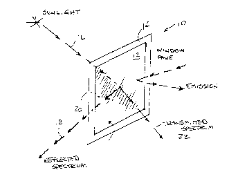
Fig. l isaschematicdiagramofatransparent panel and the reflectionand
transmission of solar energy impinging upon the panel; and
Fig. 2 is afragmentary section view of the transparent panel shown in Fig.
1'embodying the present invention.
DETAILED DESCRIPTION OF PREFERRED EMBODIMENT
For purposes of the following description, the terms "upper," "lower,"
"left," "rear," "front," "vertical," "horizontal" and derivatives of such
terms shall relate
to the invention as oriented in Figs. 1 and 2. However, it is to be understood
that the
inventionmayass<anevariousalternativeorientations,exceptwhereexpresslyspecified
to the contrary. It is also to be understood that the specific devices and
processes
illustrated in the attached drawings, and described in the following
specification are
simply exemplary embodimer~oftheinventiveconceptsdefined intheappended claims.
Specific dimensions and other physical characteristics relating to the
embodiments
disclosed herein are not to be considered as limiting, unless the claims
expressly state
otherwise.
Referringtothedrawingfigures,Fig. l schematically illustratesawindow
pane assembly 10 having a transparent panel 12 mounted in a frame 14. A beam
of
radiation 16 such as sunlight is shown impinging upon the transparent panel 12
at an
anglesubstantiallydependentupontheinclinationofthesunandtheorientationofthe
-4-
CA 02322307 2000-10-04
assembly 10. A portion 18 of beam 16 is reflected by the surface 20 while a
second
portion 22 passes and is transmitted through the panel 12. Preferably, a
substantial
portion of the infrared portion of the beam 16 is reflected as shown by
numeral 18, and
asubstantial portion ofthevisible spectrum ofthe beam 16 istransmitted as
represented
by numeral 22. The relative amounts of reflected and transmitted wavelengths
of the
spectrum can be controlled bytheangleofinclinationorangleofincidence of beam
16
upon the surface 20 relative tothenormal shownb~ referencenumera123.
Forexample,
it may be desirable to transmit greater amounts of the infrared
spectrumwhenthe angle
of incidence with respect to the normal 23 is less such as when the sun is
lowrelativeto
the horizon (winter months) than when the sun is high relative to the horizon
(summer
months). It is believed that the instant invention achieves these goals.
Fig. 2 illustrates a fragmentary cross-section of the transparent panel
assembly l0embodyingtheinventionandincludesthetransparentsubstratesuchaspanel
12 having an outer or exterior surface 20 and an inner or interior surface 24.
Substrate
12 may be made from many types of materials capable of transmitting a
substantial
portionofthespectrumrangingfromtheultra-violettotheinfrared. Conventional
glass
has been usedtoformpanei 12 and isthepreferable material for this invention
although
awiderangeofpolymericmaterialsmayalsobeusedincludingplasticsandresins. The
dimensions of panel 12 may also vary ranging from as much as more than one-
half inch
thicktoaslittleasone-sixteenthofaninch,dependinguponthedesiredapplication.The
-5-
CA 02322307 2000-10-04
dimensions in theheight andwidthwill depend greatly uponthemanufacturing
ability
of the glass producer.
In one form of the invention, an interference filter assembly (IFA) 26 is
deposited on one surface 24 ofthe panel 12. Tlie interferencefilter assembly
26 includes
atleastone,andpreferablymultiplesequences26ofmicrofinelaminations.Ingeneral,
each sequence includes abase oxide layer30 underlyingametallic alloy layer32
which,
inturn, is overlain by aprotection layer 34. It is contemplated thatafinal
durability layer
36 would be deposited ontopto protecttheunderlying oxide Iayer30,thealloy
layer32
and the protection layer 34. In a preferred embodiment such as shown in Fig.
2, two
micro fine lamination sequences 28 and 28A are provided wherein the first or
base
sequence 28 includes oxide layer 30 adjacent surface 24 ofpanel 12. Base oxide
layer
30 is overlaid by the metallic alloy layer 32 which, in turn, is covered by a
protection
layer 34. Deposited on top of protection layer 34 is a second base oxide layer
30A,
followed by a second metal alloy layer 32A which, in turn, is covered by a
second
protectionlayer34A. Terminatingthesequenceandprovidingabondingsurfaceforthe
durability layer 36 is an oxide layer 38.
Ingeneral, oxide layers 30, 30A and 38 provide abondingsurfaceforthe
adjacent components. Inotherwords,theoxidelayersprovidemolecular bonding sites
for the adjacent material. In addition, the oxide layers provide an index of
refraction
complementarytothemetalalloylayerssuchtha2certainportionsofthespectrumimpact
-6-
CA 02322307 2000-10-04
the alloy layeratashallowangle, andthevisibleportion ofthespec~um
impactthealloy
layer at a steeper angle to be transmitted there through. Suitable oxides
include those
selectedfromthegroup oftitanium dioxide(T,OZ); niobiumpentoxide(Nb205);
stannous
oxide (SI~10.~~; indium oxide; bismuth oxide andzirconium oxideand
othersdescribed in
U. S. Patent Nos. 4,462,833 and 5,563,734, the contents ofwhich are
incorporated herein
by reference. In substitution ofthe oxides describedabove, compositefilmsmay
beused
such as those selected from the group ofzirconium rlitrideand silicon
nitrideformed by
contemporaneousdeposition. Othernitrideswhichmaybesuitableincludecomposites
oftitanium nitride and silicon nitride, hafnium nitride and silicon nitride,
oramixture of
silicon nitride, aluminum nitride, zirconium nitride, titanium nitride and/ or
hafnium
nitride. Themethod ofdepositing the different combinations or composites of
nitrides
isdisclosed inU.S. Patent No. 5,563,734, the substance of which isincorporated
herein
by reference.
Generally, the thickness of the first base oxide layer 30 ranges from
approximately 50 to 300 Angstroms (~), preferably from about 75 to 200 (~),
and most
preferably from approximately 100 to 150 (~). Regarding the second and third
oxide
layers 30A and 30B, respectively, thicknesses may be ofthe same order. In the
event a
composite film is used such one or more of the nitrides mentioned above, the
layer
correspondingto numeral 30 may haveathicknessrangingpreferably from about 1
OOto
200 (~), and most preferably from approximately 125 to 200 ( fit). Subsequent
nitride
CA 02322307 2000-10-04
layers such as those corresponding to layers 30A and 30B may be within the
same
thickness range.
Deposited ontop of, and bound to base oxide layer 30 is metal layer 32.
Metal layer 32 may be deposited or applied to base layer 30 in various ways
including
sputterdepositiontoathicknessrangingfromabout200 to300(A),sufficienttoprovide
atint orcolorto panel 12 asviewed from side20, but insufficientto
blockmorethan 20%
of the visible spectrum. In one embodiment, meal layer 32 comprises an alloy
of the
noble metals gold and silver wherein silver forms the dominant component. In a
preferred embodiment, goldformsmorethan0.2 percent, but less than 0.5
percentofthe
al loy, and in the most preferred embodiment, about two to three percent. For
example,
in aprototypeofthe invention,themetal alloy layer32 includedgold and
silverwherein
gold comprised about two percent of the alloy.
Deposited on top of the metal alloy layer 32, and preventing oxidation
thereof is a protective layer 34. Protective layer 34 may be any one of a
number of
transparentmaterialswhichalsohavealowpermeabilitysuchasapolymer. Theprimary
purpose oftheprotective layer isto preventoxidation ofthemetal alloy layers.
Although
inapreferredformoftheinvention,theprotectivelayerisdepositedoverthemetal alloy
layers, polymeric materials may also be used, including a sheet adhered to
metal alloy
layer32 by anadhesive(notshown) orbonded byapplication ofheatsufficientto
render
polymer34tackyandadheretometal alloy layer32. Thicknessesforsuchlayersoffilm
_g_
CA 02322307 2000-10-04
34 may range from about 50 ~ to 100 ~1, or if made from a polymer, from about
one-
quarter to about on-half mill, and most preferably no greater than 1 to about
2 mill.
In the preferred form of the invention, the lamination sequence 28 just
described is repeated at least once to form sequence 28A. However, it is
contemplated
there may be situations where one sequence 28 is desirable. However, in the
case of
multiple sequences such as 28 and 28Ashown, each subsequentoxidelayer, such as
30A,
is deposited ontop of and bondedtothe underly~ngprotective layersuch
asrepresented
by layer 34 using the same deposition technique described above. The
deposition
methods and sequences for the metal alloy layer 32A and protective layer 34A
are
repeated. Inthepreferred embodiment,thicknesses ofthe layers in the subsequent
layer
sequences are not substantially changed from that of the initial layer
sequence.
Inthe preferred embodimentoftlie invention, the upper surface afthelayer
sequencestack(28, 28A) isprotected by durability layer36 deposited ontop
ofthefinal
oxidelayer38. Thedurabilitylayer36mayalsobeformedusingadepositiontechnique
such as one of those mentioned above, or may be a polymer sheet on top of
oxide layer
38. Polymer layer 36 is preferably much more resilient to solvents and
abrasions than
either one or both of layers 34 or 34A as layer 36 forms the primary barrier
against
cleansers and applicators. Thicknessesfor durability layer36 may also vary
depending
upon the type of material being used.
-9-
CA 02322307 2000-10-04
In an alternate form ofthe invention, metal al toy protection layers 34 and
34A may be formed from dielectric materials having indices of refraction
greater than
about 1.5, and preferably between about 2.1 and 2.9. Suitable dielectric
layers would
includethenitridesorcompositefilmsmentionedabove. Eachdiel~ctriclayermayhave
S athicknessrangingfromabout200 Auptoabout600 ~l,preferablybetweenabout250 A
and about S50 ~, and most preferably between about 250 ~t and S00 ~l.
Thicknesses may
vary as certain film compositions transmit less:visible light than others. For
these
materials, thicknesses may be reduced to improve transmittance or emissivity.
The above description is considered that of the preferred embodiments
only. Modificationsoftheinventionwilloccurtothoseskilledintheartandtothosewho
makeorusetheinvention. Therefore,itisunderstoodthattheembodimentsshowninthe
drawings and described above are merely for illustrative purposes and not
intended to
limitthescopeofthe invention, which is defined by
thefollowingclaimsasinterpreted
according to the principles of patent law, including the doctrine of
equivalents.
The embodiments of the invention in which an exclusive property or
privilege is claimed are defined as follows:
I Claim:
-10-