Note : Les descriptions sont présentées dans la langue officielle dans laquelle elles ont été soumises.
CA 02330513 2001-O1-09
1 9494
MICROBENCH AND PRODUCING METHOD THEREFOR, AND OPTICAL
SEMICONDUCTOR MODULE USING SAME
BACKGROUND OF THE INVENTION
1. Field of the Invention
The present invention relates to a microbench, which is
used to optically couple an optical fiber and an optical
semiconductor device, and a manufacturing method therefor,
and an optical semiconductor module, which is constituted
using same.
2. Description of the Related Art
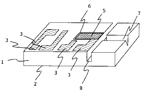
A substrate having V-groove thereon, such as that shown
in Fig. 11, has been used as a self-alignment mechanism for
the optical coupling of an optical fiber to an optical fiber,
or an optical fiber to an optical semiconductor device
(Japanese Patent :Laid-open No. H5-21817). In the figure, 1
is a silicon (Si) substrate, 2 is back surface metallization,
3 are metallized interconnects, 4 is silica insulation, 5 is
a AuSn deposited die area, 6 is an alignment mark, 7 is a V-
groove, and 8 is a dicing line. Actually, as long as the
substrate has a groove shape, it is possible to affix an
CA 02330513 2001-O1-09
' 2 9494
optical fiber to the substrate, and a trapezoid or
rectangular groove would also be capable of fully performing
this function, but because V-shaped processing has been
accurate in the past, a V-groove 7 has come to be used most
often. Ceramics substrates and Si substrates 1 have been
used as this substrate having a V-groove (Japanese Patent
Laid-open No. 7-14941). The former has primarily been
processed a dicing process, and the latter has been
processed via a dicing process, and anisotropic etching with
potassium hydroxide (KOH).
A substrate, which has this V-groove 7, and optically
couples an optical semiconductor device and an optical fiber
in a compact fashion by the V-groove 7 is called a
microbench. Among these microbenches, those that make use
of Si are called Si microbenches, and to date there have
been numerous inventions that put an Si microbench into
practice (Refer to "Packaging Technology in Lightwave
Communication" Japan Institute of Electronics Packaging
Society publication Vol. 1, No. 2, 1998).
A semiconductor laser device (laser diode (LD)) will be
used as a typical example of an optical semiconductor device,
and will be explained. An LD is lined up with an alignment
mark on an Si microbench, and is die bonded, using an AuSn
or other soldering material, to a junction down package,
which provides light-emitting, light-receiving layers on the
CA 02330513 2001-O1-09
3 9494
substrate side. The facet of an optical fiber is either
used as-is, or is used by processing the end into a lens to
enhance optical coupling efficiency. Further, there are
also cases in which a non-reflective coating is applied to
avoid the noise of mode disturbance resulting from reflected
light. This optical fiber is affixed in a groove with
either plastic or_ soldering material. With such a simple
process, it has become possible to eliminate the time
consuming, and costly laser beam welding-based aligning
process that had been deemed necessary to date ("Packaging
Technology in Lightwave Communication" Japan Institute of
Electronics Packaging Society publication Vol. 1, No. 2,
1998).
This Si microbench is manufactured using the following
process. (1) A photomask is manufactured using sub-micron
order precision. The shape of this photomask is designed so
that the center point of an optical fiber, which is a
cylindrical shape, is on the substrate surface because of
taking into account the KOH-based anisotropic etching of Si.
(2) After etching, a dicing line is formed so as to form an
optical semiconductor device mounting portion that is
orthogonal to the groove. This is because in anisotropic
etching, the vicinity of the LD mounting portion is etched
in the shape of a triangular pole, and in the state
following etching, the distance between the LD and the
CA 02330513 2001-O1-09
4 9494
optical fiber cannot be made shorter, and the purpose is for
the dicing line to bring the optical fiber right near the
semiconductor device. (3) Since the Si substrate is
conductive, silica glass is formed as an insulating layer on
parts, which are to be electrically isolated from the
semiconductor device, and thereafter, metallization is
performed for the interconnects. (4) Metallization and the
vapor deposition of an AuSn or other solder are carried out
on the semiconductor device mounting portion (die bonding
area).
An optical semiconductor module is manufactured by
combining the skeletal structure, resulting from the Si
microbench, LD and optical fiber, together with ceramics, a
leadframe, and a ;plastic body, and forming an electrical
connection (Refer to Japanese Patent Laid-open No. H9-223806,
and Japanese Patent Laid-open No. H10-200155).
In the field of optical communications, there has been
a tendency to develop large-capacity, high-speed
communications in line with the popularization of the
Internet and other means of multimedia communications.
However, in general, there is a tendency for noise to
increase when the telecommunications rate is raised, and a
more excellent signal-to-noise (S/N) ratio than in the past
is required for telecommunications systems. Meanwhile,
lowering the junction temperature of a LD and enhancing
CA 02330513 2001-O1-09
9494
light output has the advantage of improving the S/N ratio of
a signal. For this reason, there is a need for a
semiconductor system with good heat-radiating
characteristics, and a high light output LD device that
5 makes use the system.
In the meantime, in the field of the information
industry, even higher speed, higher density
recording/playback capabilities are needed. In general, a
blue or other such short wavelength LD required in a high-
density system still has low light emitting efficiency,
necessitating the improvement of the S/N ratio here as well,
and to enhance the light output of such LD, there is a need
for a high light output LD device that makes use of a system
having good heat-radiating characteristics. In particular,
even higher light output is required in a recording system
than in a playback system.
High speed is a performance capability demanded of an
LD. Operating an LD at the high speed of 10 gigabits per
second (Gbps) will make it possible to increase capacity
four-fold compared to the conventional 2.5Gbps. For this
reason, the capacitance between the substrate and the
interconnects, and the inductance of the interconnects
themselves, as well as interconnect resistance must be
lowered. Because silica is utilized in the insulating film
for a Si microbench, the thickness of the film cannot be
CA 02330513 2001-O1-09
6 9494
increased. The problem is that reducing inductance
increases the capacitance of the interconnects. According
to the disclosure in The Proceedings of the 1995 Electronics
Society Conference of IEICE on the Characteristic of High
Speed Electrical Circuit on PLC-Platform, on a Study on a
Compact Package for Multichannel Multigigabit Optical
Interconnection C179, with the object of reducing
interconnect capacitance, a thick polyimide sheet was
purposely formed cn top of an Si microbench, and
metallization for the interconnects was formed thereupon.
However, in this method, in addition to the fact that
polyimide formation had to be carried out with precision
thickness, the polyimide foamed during the die bonding of
the semiconductor device due to the pressure of absorbed
water and caused open circuits and the like, deteriorating
the yield of optical semiconductor modules.
Further, because the LD discussed here is a mass
production type, which is utilized in ordinary homes, costs
must also be lowered. The most costly part of a LD is the
Si microbench. In a case in which anisotropic etching was
performed on an Si substrate, the situation was such that
etching unevenness occurred on the inner surface, making it
almost impossible to achieve an uniform anisotropic etching
surface. This was a problem in that the optical coupling of
the optical fiber and LD could not be accomplished
CA 02330513 2001-O1-09
7 9494
satisfactorily. In Japanese Patent Application Laid-open No.
H9-90173, there is disclosed a microbench, which is
constituted by foaming a plastic using a metal, or a metal
and ceramics as filler to reduce the costs thereof. The
problem here is that in a case in which a metal was used,
interconnect capacitance increased, a polyimide sheet
process became necessary, and the yield of optical
semiconductor modules deteriorated, in the end, leading to
increased costs. Further, in a case in which a plastic was
used, in addition to the inherent problem of the [plastic]
itself foaming for the reasons explained hereinabove, the
problem was that thermal conductivity worsened, causing the
S/N ratio to deteriorate.
SUMMARY OF THE INVENTION
An object of the present invention is to manufacture
and supply a microbench for realizing a highspeed, low-cost
optical semiconductor module with a high S/N ratio.
To solve for the above-mentioned problems, the present
invention comprises the constitutions described hereinbelow.
(1) A microbench for use in mounting an optical fiber,
comprising a substrate made of a ceramics having a specific
resistance of 109 ~cm or larger and a dielectric constant of
15 or less, wherein a groove for mounting an optical fiber
CA 02330513 2001-O1-09
8 9494
is formed on the surface of the substrate, there is provided
a semiconductor device mounting portion onto which an
optical semiconductor device is mounted at the end portion
of the groove, and an alignment mark for semiconductor
device mounting is disposed in the semiconductor device
mounting portion.
(2) The microbench of the disclosure in the above-
mentioned (1), wherein said ceramics is either A1N or one
having A1N as its principal component.
(3) The microbench of the disclosures in either the
above-mentioned (1) or (2), wherein a shape of said groove
is either V-shaped or U-shaped.
(4) The microbench of the disclosures in either the
above-mentioned (1) or (2), wherein a metallic layer with a
thickness of not less than O.lmm and not more than 2mm is
disposed on either one surface or both surfaces of said
groove and said semiconductor device mounting portion.
(5) The microbench of the disclosure in the above-
mentioned (4), wherein, when said metallic layer is disposed
on the groove of the substrate, a shape of the groove is
unrestricted, and the surface of the metallic layer has a
shape of either a V or a U.
(6) The microbench of the disclosure in the above-
mentioned (4), wherein, when said metallic layer is disposed
in the semiconductor device mounting portion of the
CA 02330513 2001-O1-09
9 9494
substrate, the alignment mark on top of the substrate is
omitted, and an alignment mark is disposed on the surface of
the metallic layer instead.
(7) The microbench of one of the disclosures of the
above-mentioned (4) through (6), wherein a metal of said
metallic layer comprises A1 as its principal component.
(8) The microbench of one of the disclosures of the
above-mentioned (4) through (6), wherein a metal of said
metallic layer comprises Cu as its principal component.
(9) A microbench producing method comprising:
providing a baked ceramics substrate;
placing a die on the baked ceramics substrate, the die
having configurations, wherein at least one shapes selected
from a group of a groove for mounting an optical fiber, a
semiconductor device mounting portion and an alignment mark
is inverted; and
re-baking the baked ceramics substrate at 1,400°C or
higher.
(10) The microbench producing method of the disclosure
in the above-mentioned (9), wherein said baked ceramics
substrate comprises AlN, said die is placed thereon under a
load applied thereto, and said baked ceramics substrate is
re-baked in a non-oxidizing environment.
(11) A microbench producing method comprising:
preparing a ceramics sheet in which holes have been
CA 02330513 2001-O1-09
9494
made in an optical fiber mounting portion and another
ceramics sheet in which there are no holes;
baking both ceramics sheets placed one on top of the
other to prepare a ceramics having a groove;
5 metallizing the surface thereof to form a metalic
layer;
inserting a metal chip into either said groove or a
portion which will serve as a semiconductor device mounting
portion, or both; and
10 heating at a temperature of 150°C or higher, while at
the same time impressing the ceramics, so that an optical
fiber maunting portion, a semiconductor mounting portion,
and an alignment mark are formed in the ceramics.
(12) The microbench producing method of the disclosure
in the above-mentioned (11), wherein said ceramics sheet has
A1N as its principal component, and the baking is performed
at a temperature of 1,400°C or higher.
(13) An optical semiconductor module, wherein a
microbench of one of the disclosures of the above-mentioned
(1) through (8) is used, an optical fiber and either a light
receiving or a light emitting semiconductor device are
mounted and affixed thereto using either a solder or a resin,
and thereafter, are electrically connected to metallized
wiring on top of said microbench, and the microbench is
CA 02330513 2001-O1-09
11 9494
mounted into either a ceramics package, or a package
comprising a leadframe.
Fig. 1 is an illustration of one example of the present
invention, and a microbench is supplied by using for the
microbench substrate 1' an AlN substrate, which shows high
insulation capabilities, high radiation capabilities and low
costs, and has a specific resistance of lO9~cm or larger,
and a dielectric constant of 15 or less.
In a ceramics substrate with a specific resistance of
109~cm or larger, and a dielectric constant of 15 or less,
the metallized interconnects applied thereon excel in high
frequency characteristics. In the ceramics substrate with a
specific resistance of 109~cm or larger, power leakage from
interconnects can be neglected. Thus, for this ceramics
substrate 1', it is not necessary to form a silica
insulation layer 4 as with a conventional Si substrate.
When the silica on a Si substrate is made thick, the silica
layer can peel off and/or cracks can occur, and as such, it
is necessary to keep this silica layer thickness to less
than 2~.m as far as possible. For this ceramics substrate,
it is possible to process same with a thickness of 2mm or
more, enabling the substrate to be made around 1,000-times
thicker than the silica of the insulation layer. Since the
dielectric constant of the silica is around 3, in the
ceramics substrate with a dielectric constant of 15 or less,
CA 02330513 2001-O1-09
12 9494
the width of interconnects in a high-frequency impedance-
matching circuit, like a microstrip line, can be steadily
widened, thus making it possible to reduce interconnect
resistance. Further, stray capacitance was generated from
the bonding pads of wires, causing high-frequency
disturbance, but this, too, can be kept small by making the
substrate thick. Thus, it is possible to prevent the
deterioration of the S/N ratio resulting from high-frequency
disturbances.
The thermal conductivity of the A1N ceramics substrate,
which also satisfies the above-mentioned characteristics, is
170W/mk or higher compared to 140W/mk for Si, and the A1N
ceramics substrate has much higher heat-radiating
capabilities. Thus, it is possible to enhance light output
by lowering the junction temperature of an LD. Furthermore,
the dielectric loss tangent (tanb), which indicates power
loss, is less than 10-' for the A1N ceramics substrate
compared to around 10-z for a polyimide film, meaning that
the A1N ceramics substrate has good high frequency transfer
characteristics, and that the S/N ratio can be improved
based thereon.
The shape of the groove for mounting an optical fiber
can be either a V-shape or a U-shape, but in a case in which
a metallic layer is disposed in the groove, as long as the
CA 02330513 2001-O1-09
13 9494
surface of the metallic layer is either a V-shape or a U-
shape, the shape of the groove is unrestricted.
A metallic layer of not less than O.lmm and not more
than 2mm thickness is provided on either one surface or both
surfaces of the groove and the semiconductor device mounting
portion, but this is to shape the groove by using the
plastic deformation of the metal, and processing is
performed after providing a metallic layer thinly when there
is a shape formed on the substrate itself, and thickly when
there is no particular shape thereon.
Accordingly, the thickness of the metallic layer is
made to range between O.lmm and 2mm. As the material, a
metal including A1 or Cu as the principal component is
appropriate. Fig. 2 is a diagram in which a circular
cylinder/optical (fiber is mounted in a V-groove, and Fig. 3
is a diagram in which metallization is applied to a V-groove,
and a circular cylinder/optical fiber is mounted therein.
Fig. 4 i.s a diagram in which A1 is filled into a groove, a
U-groove is formed therein, and a circular cylinder/optical
fiber is mounted therein, and Fig. 5 is a similar diagram in
which Cu is filled into the groove.
An alignment mark for mounting a semiconductor is
disposed in an optical semiconductor device mounting portion,
but in a case in which the above-mentioned metallic layer is
provided, the alignment mark on the ceramic substrate is
CA 02330513 2001-O1-09
14 9494
omitted, and an alignment mark is provided on the surface of
the metallic layer instead. Fig. 6 is an example in which
alignment mark 6 is provided on substrate 1', and metallic
layer 9 is provided as-is, and Fig. 7 is an example in which
alignment mark 6 is omitted on substrate 1', and alignment
mark 6 is provided on metallic layer 9.
To couple optically an optical device with an optical
fiber on a microbench, positioning accuracy must be
submicron-3E,im. This is because the core diameter of an
optical fiber is 10~,m, and approximately 1/3 or more of LD
light is incident on the optical fiber. Positioning
accuracy in the height direction is only necessary for the
distance between the die bonding area and the center of a
facet of an optical fiber circumscribed by the groove, and
the permissible tolerance is submicron-3~,m for this as well.
Because an alignment mark can be aligned with the light
emitting/receiving parts of an optical semiconductor device
at a tolerance of submicron or less, positioning accuracy in
the horizontal direction is only necessary for the distance
from the alignment mark to the center of a facet of an
optical fiber circumscribed by the groove, and this
permissible tolerance is also submicron-3~un. Since the
angle of the light that can be incident in an optical fiber
can be up to around +-10 degrees from a vertical line drawn
to a facet of the optical fiber, the gradient of the groove
CA 02330513 2001-O1-09
15 9494
and die bonding area must be held to within +-3 degrees.
Accordingly, a method in which a super hard metal die is
used for microprocessing is appropriate. The super hard
metal die is a metal die that was processed having Mo or WC
as a raw materials and is capable of three-dimensional
molding at tolerances of submicron or less.
The following 2 kinds of molding methods, which utilize
this metal die, can be conceived.
One is a method in which a metal die is pressed
directly against the ceramics substrate after baking in a
high-temperature environment, and the groove is processed by
deforming the ceramics substrate itself. Fig. 8 shows a
photograph of a ceramics surface after processing. It is
clear from this photograph that the surface finish is smooth.
In this method, a temperature of 1,400°C or higher is
necessary in an oxygen-purged nitrogen environment, and
thereafter, producing a module can be performed easily by
simply metallizing the interconnects and back surface.
The other one is a method in which the metal die is
pressed against the ceramics substrate after bonding a Cu or
A1 metallic chip susceptible to plastic deformation in a
location where deformation is necessary. In this producing
method, there is the addition of a process for bonding a
metallic chip, but molding is possible from ordinary
temperature to around 300°C. Here, the Young's modulus of
CA 02330513 2001-O1-09
16 9494
A1 is high, and high processing precision is required of the
super hard metal die. Further, the coefficient of thermal
expansion is a large 23X10-6/degC, and the thickness of the
A1 layer cannot be made thick due to the unconformability of
thermal expansion, but this method is advantageous in that
producing is facilitated since A1 is susceptible to plastic
deformation even at low temperatures approaching ordinary
temperature. Since the Young's modulus of Cu is low, super
hard metal die processing is easy, but processing must be
done at a high temperature of over 250°C, where plastic
deformation readi:Ly occurs. The coefficient of thermal
expansion of Cu is a small 18X10-6/degC, and in addition to
the unconformability of thermal expansion being smaller than
that for aluminum, it is electrically superior, having
electric conductivity that is around 1.5-times that of A1.
As a formation for the groove, when baking an A1N
ceramics, it is possible to make a rectangular
parallelepiped groove, which is one size larger than an
optical fiber, and into which a metallic chip is inserted
beforehand. The substrate outfitted with this large
rectangular parallelepiped groove can be manufactured by
laminating a ceramics temporary compact sheet with holes
therein and a ceramics temporary compact sheet with no holes,
and baking same. When molding is performed after bonding an
A1 or other metallic portion thereupon, high-precision
CA 02330513 2001-O1-09
17 9494
groove can be easily processed. The groove cross-section at
this time constitutes a 2-layer structure of ceramics and
metal.
During these processes, high precision submicron
positioning accuracy becomes possible by building into the
metal di.e in advance the die bonding area (the semiconductor
device mounting portion), the alignment mark, and the groove.
Sometimes a curvature will be formed at the end face of the
groove at the part, where the die bonding area and the
groove make contact, and the precision for accurately
installing an optical fiber worsens. Accordingly, this part
is removed by dicing.
In a case in which an optical module is manufactured
using an AlN microbench, there are cases in which a
leadframe is used. To achieve strength of adhesive bonding
of the l.eadframe and A1 wires at this time, A1 spot vapor
deposition is utilized. When manufacturing the A1N
microbench, the A1N substrate, which has the groove that is
one size larger than an optical fiber, and a leadframe are
bonded, and thereafter, using Al spot vapor deposition, the
A1 portion can be simultaneously formed on both a wire
bonding pad and the groove, prior to die molding. Using
this method enables costs to be reduced.
CA 02330513 2001-O1-09
18 9494
Using this A1N microbench to produce an optical module
enables the high yield manufacture of a highspeed, low-cost
optical semiconductor module with a high S/N ratio.
In particular, producing an optical semiconductor
module using the A1N microbench, which utilizes A1 vapor
deposition and a leadframe, makes it possible to produce an
optical semiconductor module at yet lower costs by using A1
wires.
BRIEF DESCRIPTION OF THE DRAWINGS
Fig. 1 is an external view of an A1N microbench of the
present invention;
Fig. 2 is an illustration of a state in which a
circular cylinder/optical fiber is mounted in a groove;
Fig. 3 is an illustration of a state in which
metallization is applied to a groove, and a circular
cylinder/optical ffiber is mounted therein;
Fig. 4 is an illustration of a state in which an A1
metal is filled into a groove, and a circular
cylinder/optical ffiber is mounted therein;
Fig. 5 is an illustration of a state in which a Cu
metal is filled into a groove, and a circular
cylinder/optical fiber is mounted therein;
CA 02330513 2001-O1-09
19 9494
Fig'. 6 is a schematic diagram of an example of an
alignment mark;
Fig. 7 is a schematic diagram of another example of an
alignment mark;
Fig. 8 is an enlarged microscope photograph of a groove
portion of an embodiment;
Fig. 9 is a schematic diagram of the preparation of an
optical semiconductor module of the present invention;
Fig. 10 is a schematic diagram of a completed optical
semiconductor module of the present invention; and
Fig. 11 is an external view of a conventional Si
microbench.
DESCRIPTION OF THE PREFERRED EMBODIMENTS
The present invention will be explained in detail
hereinbelow in accordance with the examples.
Example 1
A1N was used as the ceramics. An A1N substrate with a
thermal conductivity of 170W/mk was used. Substrate
thickness was 0.5mm, and the substrate was baked and used
as-is without polishing. The size of the substrate was 40mm
x 60mm. A metal die was combined with a chip processed with
Mo, and was shaped in a plate having protrusions on a 50mm x
70mm surface. Here protrusions could be taken to mean a
CA 02330513 2001-O1-09
20 9494
groove, an alignment mark, and a die bonding area, but only
a groove and an alignment mark were used here. The A1N
substrate and the metal die were placed one on top of the
other, and placed on top of a Mo plate. A lOkg weight was
placed an top of the metal die. This was placed in a high-
temperature furnace with a nitrogen environment, and the
substrate was formed in a 1,400°C environment. A sink of
the metal die was adjusted for by making the peripheral
portion of the die thick. Fig. 8 shows a photograph of the
finished substrate at this time. The ability to process at
submicran surface roughness precision was confirmed.
Processing precision, which can adequately align an
optical device and an optical fiber, is achievable even as-
is, but processing precision can be enhanced further by
measuring the depth of the groove, and thereafter, polishing
the A1N substrate.
At this point, the contact portion of the die bonding
area and the groove was removed by dicing, and an optical
fiber was accurately installed up to the end face of an
optical device.
The surface (back surface) on which there was no groove
of the die-formed substrate was polished, the thickness of
the substrate was processed to 0.3mm, a W/Mo/Ni was
metalli~ed over the entire surface by vapor deposition, and
thereafter, a Ni/Au was plated. On the groove processed
CA 02330513 2001-O1-09
21 9494
surface of the die-formed A1N substrate, a photomask was
used, and Ti/Pt/Au metallized interconnect was processed via
vapor deposition. Signal interconnects were constituted of
a microstrip line structure. For impedance matching
resistance, a thin film of Cr was used, and the resistance
value was adjusted by trimming. Vapor deposition was used
to deposit 3~,rm of AuSn onto a LD mounting portion on top of
the A1N microbench. An optical fiber is affixed with resin
to the groove of the A1N substrate that did not undergo
metallization (Fig. 2). This is to increase the strength of
adhesive bonding. For an A1N substrate with a metallized
groove (Fig. 3), an optical fiber can be affixed with either
solder or resin, but soldering makes possible a stronger
bond. Cutting this A1N substrate to a 4mm x 6mm size using
dicing completed the A1N microbench.
First, a LD was die bonded junction down on top of the
A1N microbench. The LD was a distribution feed-back (DFB)
laser diode with a built-in modulator. The electrode pad
for signals was made as small as possible. An alignment
mark in the die bonding area and a mark on the back surface
of the LD (side that does not have an active layer) were
matched up at this time. Next, an AuSn pre-form was used to
die bond a light receiving device. This light receiving
device is for monitoring the light output of the LD.
Furthermore, a facet of the optical fiber was temporarily
CA 02330513 2001-O1-09
22 9494
affixed in a manner, which brought it as close to the LD as
possible, and an ultraviolet light hardening resin for
index-matching was applied to the groove. Ultraviolet light
was applied to the plastic, and the optical fiber, the
periphery of which had been coated with Ti/Pt/Au, was
affixed. The metallization of the optical fiber was for use
in subsequent soldering.
This temporary compact was die bonded using PbSn to a
butterfly-type flat package, which utilizes 10 alumina
ceramics pins. From the standpoints of thermal expansion
matching and radiation capabilities, it is desirable that
this ceramics be A1N. At this time, the optical fiber,
which had been attached with a metal guide, was run outside
of the package via an optical fiber transmission hole, which
existed in the butterfly flat package beforehand. At die
bonding, solder was applied to the optical fiber, and the
guide was soldered to the package together. At this point
in time, the package was made sufficiently airtight. An
electrical connection was made using wire bonding, and
thereafter, a cap was applied by seam welding, and an
optical semiconductor module was completed.
This optical semiconductor module was confirmed to have
a good S/N ratio, and to be capable of satisfactory
operation at a high speed of lOGbps.
Example 2
CA 02330513 2001-O1-09
23 9494
An A1N ceramics (AlN) substrate with a thermal
conductivity of 170W/mk was used. The A1N producing method
will be explained. First, AlN powder, a glass auxiliary,
and a plastic binder were mixed together with an organic
solvent, and a sheet was formed. This sheet was dried, and
made into a plate, that was a temporary compact. For one
plate, press was used to open a longitudinal hole 0.3mm or
more in width, and another hole-less plate was laminated
thereto. This plate was baked at 1,700°C in a nitrogen
environment, and a substrate was completed. The substrate
thickness was 0.7mm.
The size of the A1N substrate after baking was 40mm x
40mm. A method for bonding either a Cu or an A1 metal plate
to this A1N substrate will be described. In the case of Cu,
first, a photomask was used to apply Ti/Mo/Ni metallization
to the A1N substrate surface on which there was the 0.3mm
wide graove, and then NiP was plated. Thereafter, a O.lmmt-
thick Cu chip was mounted on a die bonding area, and a
0.2mmt-thick Cu chip was mounted on the groove portion, and
the Cu was bonded to the A1N substrate by heating in a
hydrogen environment. In this case, the Ni and Ni-plated Cu
can be bonded with silver solder. Thereafter, the die
bonding area, an alignment mark, and the groove were
simultaneously formed by pressing the metal with a super
hard metal die of tungsten carbide. In this case, there was
CA 02330513 2001-O1-09
24 9494
one die, and a plurality of grooves on the entire surface of
the substrate was processed by substrate feed. The
processing temperature can be ordinary temperature, but it
is desirable to process at 150°C or higher. Thereafter,
gold was plated on all metallized surfaces, and thereafter,
AuSn vapor was deposited, and an A1N microbench was
completed.
In a case in which A1 was used, first, A1 spot vapor
deposition was performed on a groove portion and a die
bonding area. A1 was also deposited via vapor deposition on
a wire bonding pad at this time. Thereafter, an AlSi
soldering material was used to mount a 0.15mmt-thick A1 chip
to the die bonding area, and a 0.15mmt-thick A1 chip to the
groove portion, and the A1 chips were bonded by heating in a
high vacuum. Instead of a soldering material, either AlSi
or Si can be deposited by vapor deposition on one side of an
A1 chip. Further, an alignment mark can also be formed on
Ni metallization without bonding an A1 chip to the die
bonding area, or A1 vapor deposition. Thereafter, the die
bonding area, an alignment mark, and the groove were
simultaneously formed by pressing with a super hard metal
die of tungsten carbide. Here, in this case, there was one
die, and press for a plurality of grooves on the entire
surface of the substrate was implemented by substrate feed.
The processing temperature can be ordinary temperature, but
CA 02330513 2001-O1-09
25 9494
it is desirable to press at around 300°C. A photomask was
used to metallize Ti/Pt/Au to the A1N substrate surface on
which there was the groove, 3~m of AuSn was deposited by
vapor deposition on the LD mounting portion, and an A1N
microbench was completed.
First, a Fabry-Perot (FP) LD was die bonded junction
down on top of the A1N microbench. The alignment mark in
the die bonding area and a mark on the back surface of the
LD (side that does not have an active layer) were matched up
at this time. Next, an AuSn pre-form was used to die bond a
light receiving device (Refer to Fig. 9). This light
receiving device is for monitoring the light output of the
LD. Furthermore, a facet of the optical fiber was
temporarily affixed in a manner, which brought it as close
to the hD as possible, and the optical fiber was affixed
using a soldering material. Characteristics are improved by
lens processing, a non-reflective coating, or a diagonal
polishing on a facet of the optical fiber.
Thereafter, Si gel was applied on an optical
semiconductor device and the optical fiber mounting portion,
and after hardening, molding with an epoxy resin, and an
optical semiconductor module was completed (Refer to Fig.
10).
In addition to making it possible to lower the cost of
a microbench, a drop in yield caused by polyimide foaming
CA 02330513 2001-O1-09
26 9494
and the like did not occur, and an optical semiconductor
module could be satisfactorily produced. It was confirmed
that this optical semiconductor module had a high S/N ratio,
had improved light output that is 3~ better than that of a
Si microbench, and operated satisfactorily at a high speed
of 2.5Gbps.
By skillfully bonding and combining either Cu or A1
with a ceramics, in particular an A1N ceramics, with a
specific resistance of 109~cm or larger and a dielectric
constant. of 15 or less, it is possible to manufacture and
supply an A1N microbench for an optical semiconductor module.
In addition to making it possible to lower the cost of a
microbench, a drop in yield caused by polyimide foaming and
the likes did not occur, and an optical semiconductor module
could be satisfactorily manufactured.
Further, this optical semiconductor module was
confirmed to have a good S/N ratio, to have light output
that is 3$ higher than that of a Si microbench, and to
operate satisfactorily at a high speed of 2.5Gbps. In a
case in which a butterfly-type flat package made of ceramics
was used, it was possible to achieve highspeed operation of
lOGbps.
It is possible to manufacture and supply a microbench
for achieving a highspeed, low-cost optical semiconductor
module with a high S/N ratio.