Note : Les descriptions sont présentées dans la langue officielle dans laquelle elles ont été soumises.
CA 02337223 2001-O1-09
WO 00/63728 PCT/US00/10072
DUAL TRANSMISSION BAND INTERFERENCE FILTER
The present application claims the benefit of U.S. Provision Patent
Application
Serial No. 60/130,212, filed April 20, 1999.
FIELD OF THE INVENTION
The present invention relates generally to optical interference filters and
more
particularly to a dual band optical interference filter capable of
transmitting optical
channels within a first and second passbands.
BACKGROUND OF THE INVENTION
Optical interference filters rely on principles of interference that modify
the
intensities of the reflected light incident on a surface. A familiar example
of interference
is the colors created when light reflects from a thin layer of oil floating on
water. Briefly
stated, by modifying the interface of a substance and its environment with a
third
material, reflectivity of the substance can be significantly altered. This
principle is used in
the fabrication of optical interference filters. These filters can be used as
one of, or as the
main filtering element in optical addldrop multiplexers employed in optical
communication systems to select one or more channels from a transmission
signal.
In its most simple form, an optical interference filter includes a cavity
which is
l5 comprised of two partial reflectors (or mirrors) separated by a spacer. The
number of
spacers determines the number of cavities of the filter. Each partial
reflector, also
referred to as a quarter-wave stack, is typically constructed by depositing
alternating
layers of high and low refractive index dielectric materials upon a substrate
where each
layer has an optical thickness (defined as: physical thickness x refractive
index) of a
CA 02337223 2001-O1-09
WO 00/63728 PCT/LJS00/10072
quarter wave (a,/4) (or odd multiple of a quarter wave) at the desired
wavelength ~,o of the
filter. Exemplary high and low refractive index dielectric materials are Ti02,
Ta205 and
Si02, respectively. The spacer is typically a half-wave (or multiple half-
wave) layer of
low refractive index material e(~. ., SiOz). An interference filter has an
associated
transmission characteristic which is a function of the reflectance of the
layers of high and
low index materials associated with the stack.
In many applications, optical interference filters are constructed using
multiple
cavities. Typically, cavities are deposited on top of other cavities, with a
quarter-wave
layer of low index material therebetween. Multicavity filters produce
transmissian spectra
to that are preferred in optical communication systems where steep slopes and
square
passbands are needed to select one or more optical channels. The larger the
number of
cavities employed, the steeper the slope of the transmission bandwidth
associated with a
particular filter. The transmission bandwidth of a multicavity filter is wider
as compared
with the transmission bandwidth associated with a single cavity filter.
:l5 FIG. 1 illustrates an exemplary transmission spectrum for a mirror
comprising a
plurality of high/low refractive index dielectric layers. The mirror exhibits
high
reflectivity at a stopband centered at 7~o and rippled sidelobes including
points A, B and
C.
FIG. 2 is an exemplary transmission spectrum for a single cavity optical
0 interference filter utilizing a pair of stacks each having the transmission
spectrum shown
in Fig. 1. As can be seen in FIG.2 the transmission response is acceptable at
wavelength
~,o (approximately 1550nm). However, the response at wavelength ~,l
(approximately
l3lOnm) falls on the sidelobe and/or within the ripple band of the
transmission spectrum,
thereby making transmission of a particular wavelength in this range
unreliable. More
CA 02337223 2001-O1-09
WO 00/63728 PCT/US00/10072
specifically, the single cavity interference filter produces high
transmittance at
wavelengths referenced at points A and B, but also produces relatively low
transmittance
as referenced at point C. Thus, transmission at a first wavelength ~,o may be
reliable while
transmission for wavelength ~,, within the ripple band or sidelobe slope are
subject to
variations in the transmission characteristic. This is also true for
wavelengths in the
1625nm range. FIG. 2 demonstrates that interference filters typically provide
a single
reliable transmission band.
As noted above, optical systems can utilize one or more interference filters
to
select particular channels from a transmission signal. For example, a first
filter may be
used to select a pay-load channel associated with voice and/or data
transmission in the
l.Sp,m range and a second filter is used to select a service channel in the
1.3~.m or 1.6~,m
range which carries system level and/or network monitoring information. The
use of two
separate filters, however, has several disadvantages. First, it increases
overall system cost
since it requires the manufacture and installation of two individual
components.
Secondly, optical networks typically have a predetermined loss budget, if
exceeded, can
compromise signal integrity. Each component, in this case an optical filter,
contributes
some loss to the overall network. By using two separate filters to select a
payload
channel and a service channel, each filter negatively impacts a network's loss
budget.
Thus, there is a need for a filtering element used with optical communication
systems capable of selecting a first and a second optical passbands. There is
a further
need to provide such a filtering element which reliably selects at least one
wavelength
corresponding to a payload channel as well as a wavelength corresponding to a
service
channel within an optical network.
CA 02337223 2001-O1-09
WO 00/63728 PCT/I1S00/10072
BRIEF DESCRIPTION OF THE DRAWINGS
Advantages of the present invention will be apparent from the following
detailed
description of the presently preferred embodiments thereof, which description
should be
considered in conjunctiowwith the accompanying drawings in which:
Fig. 1 illustrates a transmission spectrum of a conventional mirror including
a
plurality of dielectric layers;
Fig. 2 illustrates a transmission spectrum of a single cavity filter including
conventional mirrors;
Fig. 3(a) illustrates a single-cavity interference filter consistent with the
present
l0 invention;
Fig. 3(b) illustrates a dual-cavity interference filter consistent with the
present
invention;
Fig. 3(c) illustrates a three cavity interference filter consistent with the
present
invention;
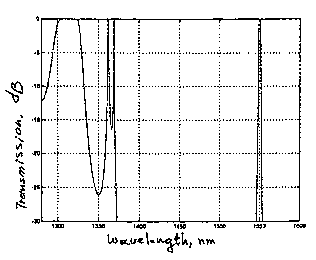
15 Fig. 4 illustrates a transmission characteristic of an exemplary triple
cavity
interference filter having a narrow transmission band at a wavelength around
1550 nm
and a broad transmission band at a wavelength around 1310 nm;
Fig. 5 illustrates schematically a mirror having q dielectric layers of
alternating
high and low refractive indices;
20 Fig. 6 illustrates a transmission characteristic associated with the mirror
shown in
Fig. 5;
Fig. 7 illustrates the refractive index of each of the layers of an exemplary
mirror
utilizing the structure described in Fig. 5;
4
CA 02337223 2001-O1-09
WO 00/63728 PCTIUS00/10072
Fig. 8 illustrates a transmission characteristic of a three cavity filter
consistent
with the present invention;
Fig. 9 a composite dielectric layer consistent with an aspect of the present
invention;
Figs. 10(a) and 10(b) illustrate a transmission characteristic and structure,
respectively, of a two-material mirror consistent with an aspect of the
present invention;
and
Fig. 11 illustrates a transmission characteristic of a three-cavity filter
using the
mirror shown in Fig. 10(b).
DETAILED DESCRIPTION
The interference filter in accordance with the present invention transmits a
narrow
(=lnm wide) wavelength band around a first center wavelength ~.o e(~. ., ~,o~
1550nm)
along with a broader (=20nm wide) wavelength band around a second center
wavelength
~,1, Le.g., ~,i= 1310nm). This can best be explained with reference to a
multilayer
dielectric mirror with sufficiently high and broad transmission band around
wavelength
~,,. The high transmission peaks (referenced at points A and B in Fig. 1) are
positioned
within the passband of the multilayer dielectric mirror corresponding to
wavelength ~,1
which is the center wavelength of the second broad band. If the first high
transmission
peak is chosen to coincide with ~,~ i.e., peak referenced at A) the following
equations can
be used to determine the parameters of the basic multilayer dielectric mirror:
_ ~ 'f" ~ ~1)
"L C~1~ ~ 1
CA 02337223 2001-O1-09
WO 00/63728 PCT/US00/10072
sin ~ ~~ Z.
Sin ~
where nH(~,~) and nL (~,1) are high and low refractive indices at ~,I; r is
the absolute value
of the magnitude Fresnel reflection coefficient for the boundary between the
high and low
index layers; and q is the number of layers in the stack or mirror. Equations
(1) and (2)
can be satisfied, for example, with nH(~,,) =2.05 (Ta505), nL(~,~) =1.44
(Si02), ~,o =
1550nm, ~,, = 1310nm, and q = 13. In this manner, for a wavelength ~,o
(=1550nm),
broad band transmission is achieved for a wavelength centered at ~,~ (=1310nm)
as well as
narrow band transmission at wavelength ~,o.
Turning to the drawings in which like reference characters indicate the same
or
similar elements in each of the several views, Fig. 3(a) schematically
describes a single-
cavity interference filter in accordance with the present invention comprising
a spacer 30
interposed between a first and second mirrors 25 and 26. Fig. 3(b) illustrates
a dual
cavity interference filter 40 having a coupling layer 70 interposed between a
first cavity
45 and a second cavity 75. Coupling layer 70 can be, for example, a low index
material
having a quarter wave optical thickness. First cavity 45 includes mirrors 50
and 60
separated by spacer 55. Second cavity 75 includes mirrors 80 and 90 separated
by spacer
85. Similarly, Fig. 3(c) illustrates a triple cavity interference filter 100
having a first
cavity 105, a second cavity 110 and a third cavity 115. First coupling layer
106 is
positioned between first cavity 105 and second cavity 110. Second coupling
layer 117 is
positioned between second cavity 110 and third cavity 115. First cavity 105
comprises
mirrors 102 and 103 separated by spacer 104. Second cavity 110 includes
mirrors 111
6
CA 02337223 2001-O1-09
WO 00/63728 PCT/US00/10072
and 113 separated by spacer 112. Third cavity 115 includes mirrors 118 and 120
separated by spacer 119.
Fig. 4 illustrates a transmission characteristic of an exemplary triple cavity
interference filter having a narrow transmission band at wavelength ~,o
(around 1550nm)
and a broad transmission band at wavelength 7~~ (around 1310nm).
The interference filter described above has the properties which allow it to
transmit both a narrow band centered at wavelength ~,o (= 1550nm) and a broad
band at
wavelength ~., (= 1310nm). However, this embodiment transmits the bands for a
particular wavelength ~,o. If a different wavelength, for example ~,a~ O, is
selected within
the TTU channel grid and the gain band of an erbium doped fiber amplifier
(1530-
1570nm), the broad transmission band centered around ~,~ would shift from
1310nm
proportionally with O, the difference between ~,o and 1550nm. The broad
transmission
band centered around ~,~ (for example, 1310nm) can be maintained for different
values of
~,o, if the high transmission region in the pass band of the multilayer
dielectric mirror is
IS greater than 20nm, which is sufficient to provide the dual band
characteristics for a fixed
pair of ~,o and ~,~.
The high transmission band around wavelength ~,, associated with the mirror
shown in Fig. 1 can be broadened by collapsing the adjacent transmission peaks
A and B
and eliminating low transmission point C. This is achieved by depositing a
dielectric
material having a refractive index nH1 = 1.55 -1.58 for the third layer as
well as for the q-
2 layer in the mirror. For example, Fig 5 illustrates a mirror having q
dielectric layers of
alternating high (H) and low (L) refractive indices. The third layer and the q-
2 layer have
an associated refractive index of = 1.55 - 1.58. Fig. 6 illustrates a
transmission
CA 02337223 2001-O1-09
WO 00/63728 PCT/US00/1007Z
characteristic associated with this mirror structure resulting in a broader
transmission
band around wavelength ~.~ (=1310nm).
Fig. 7 graphically illustrates the refractive index of each of 17 layers
{q=17) of an
exemplary mirror utilizing the structure described with reference to Figs. 5
and 6. TaZ05
(nH = 2.05) was selected as the high refractive index material for layers 1,
5, 7, g, 11, 13
and I7. Si02 (nH = 1.44) was selected as the low refractive index material for
layers 2, 4,
6, 8, 10, 12, 14 and 16. Layers 3 and 15 have refractive index n,~~ = 1.58.
Layers 3 and
15 may be deposited either by a properly ratioed co-deposition of high and low
index
materials, or by depositing materials having a refractive index of 1.58 e(~. .
., mullite,
which is a mixture of 76-80% of A1203 and 20-24% of Si02).
A three cavity interference filter having the structure described with
reference to
Fig. 3(c) where each mirror (102, 103, 111, 113, 118 and 120) is formed using
the
structure described in Figs. 5-7. A transmission characteristic associated
with this three
cavity filter is shown in Fig. 8. As can be seen, the 1 lOnm broad
transmission band
15 around wavelength ~,I (=1310nm) allows a choice of wavelengths ~,o within
the gain band
of a typical erbium doped fiber amplifier (1520nm - 15?Onm) without
sacrificing
transmission around wavelength ~,~.
The interference filter described above calls for the deposition of a third
material
having an intermediate refractive index value in the range of 1.55-1.58 with
respect to the
2o high and low refractive index materials forming each mirror. However, the
introduction
of this third material into the deposition process is less desirable from a
manufacturing
perspective. Accordingly, the third material having an intermediate refractive
index used
to form layers 3 and q-2 (e.g. layers 3 and 15 referenced in Fig. 7) of an
exemplary minor
CA 02337223 2001-O1-09
WO 00/63728 PCT/ITS00l10072
can be formed by a symmetrical composite consisting of a layer of high index
material
(e.g., Ta205, nH.2.05) clad by a pair of low index material layers (-e.g.,
Si02, nL = 1.44) as
schematically shown in Fig. 9. This composite material has an optical
thickness of one
quarter wave at 7v,o, and its effective refractive index is 1.58. If ~
represents the optical
thickness (in quarter waves at ~,o) of the thin high index layer comprising
the composite,
the optical thicknesses 8L of the low index material can be calculated as
follows:
. Z /l M ~ !7L
~ z. ~ n Z ~ n rT' ' ~~y
a. _
z
The resulting structure has an optical thickness of one quarter wave at ~,o
and allows the
use of turning point monitoring for quarter waves during layer deposition.
Figs. 10{a) and 10(b) show a transmission characteristic and the structure,
respectively, of the two-material minor with essentially identical
characteristics to a three
material mirror design (Figs. 6-7). In this example, 8H= 0.14 and SL = 0.4257.
It should
be noted, that the cladding layers of Fig. 9 with optical thicknesses of
0.4257 (7v,/4) joining
the one ~./4 thick low index material layers surrounding the original layer
with
intermediate refractive index nH,= 1.58, forms low index layers of 1.4257 ~,/4
optical
thickness at 7~,0.
Fig. 11 illustrates a transmission characteristic of a three cavity filter
using the
2o two-material mirror structure described above. As can be seen, the broad
transmission
band around wavelength ~,, (=1310nm) allows a choice of wavelengths ~,o within
the gain
9
CA 02337223 2001-O1-09
WO 00/63728 PCT/US00/10072
band of a typical erbium doped fiber amplifier (1520nm - 1570nm) without
sacrificing
transmission around wavelength ~,1.
Consistent with a further aspect of the present invention, the third layer
shown in
Fig. lOb can be eliminated and the optical thickness of both the second and
fourth layers
can be increased to have an optical thickness of 1.5 times a quarter
wavelength to form a
single continuous layer having an optical thickness of 3/a a quarter
wavelength. Likewise,
the q-2 layer can be eliminated and the optical thickness of the q-1 and q-3
layers can be
increased to have an optical thickness of 1.5 times a quarter wavelength to
form a single
continuous layer also having an optical thickness of 3/4 a quarter wavelength.
While the foregoing invention has been described in terms of the embodiments
discussed above, numerous variations are possible. Accordingly, modifications
and
changes such as those suggested above, but not limited thereto, are considered
to be
within the scope of the following claims.
l0