Note : Les descriptions sont présentées dans la langue officielle dans laquelle elles ont été soumises.
CA 02339114 2001-O1-30
WO 00/06506 PCT/US99/16178
METHOD OF FABRICATING PHOTONIC STRUCTURES
This application claims the benefit of U. S. provisional application
60/094,609, filed July 30, 1998.
Background of the Invention
The invention relates to a method of making photonic crystals and
passive components comprising photonic crystals. In particular, the method
includes one or more extrusion steps to produce a cellular or channeled object
followed by a step of viscously sintering the object. The sintered, channeled
object is heated and drawn to a final diameter.
A photonic crystal is a structure having a periodic variation in dielectric
constant. The periodic structure may be 1, 2 or 3 dimensional. The photonic
crystal allows passage of certain light wavelengths and prevents passage of
certain other light wavelengths. Thus the photonic crystals are said to have
allowed light wavelength bands and band gaps which define the wavelength
bands which are excluded from the crystal.
At present, the wavelengths of interest for telecommunication
applications are in the range of about 800 nm to 1800 nm. Of particular
interest is the wavelength band in the range of about 1300 nm to 1600 nm.
Light having a wavelength in the band gap may not pass through the
photonic crystal. Light having a wavelength in bands above and below the
band gap may propagate through the crystal. A photonic crystal exhibits a set
CA 02339114 2001-O1-30
WO 00/06506 PCT/US99/16178
2
of band gaps which are analogous to the solutions of the Bragg scattering
equation. The band gaps are determined by the pattern and period of the
variation in dielectric constant. Thus the periodic array of variation in
dielectric
constant acts as a Bragg scatterer of light of certain wavelengths in analogy
with the Bragg scattering of x-rays wavelengths by atoms in a lattice.
Introducing defects into the periodic variation of the photonic crystal
dielectric constant can alter allowed or non-allowed light wavelengths which
can propagate in the crystal. Light which cannot propagate in the photonic
crystal but can propagate in the defect region will be trapped in the defect
region. Thus, a point defect within the crystal can serve as a localized
"light
cavity". Analogously, a line defect in the photonic crystal can act as a
waveguide for a mode having a wavelength in the band gap, the crystal lattice
serving to confine the guided light to the defect line in the crystal. A
particular
line defect in a three dimensional photonic crystal would act as a waveguide
channel, for light wavelengths in the band gap. A review of the structure and
function of photonic crystals is found in, "Photonic Crystals: putting a new
twist
on light", Nature, vol. 386, March 13, 1997, pp. 143 -149, Joannopoulos et al.
A first order band gap phenomenon is observed when the period of the
variation in dielectric constant is of the order of the light wavelength which
is to
undergo Bragg scattering. Thus, for the wavelengths of interest, i.e., in the
range of about 1300 nm to 1600 nm, as set forth above, a first order band gap
is achieved when the period of the variation is about 500 nm. However,
photonic crystal effects can occur in crystals having dielectric periodicity
in the
range of about 0.1 pm to 5 pm. A two or three dimensional photonic crystal
having even this larger spacial periodicity is difficult to fabricate.
In U. S. patent 5,774,779, Tuchinskiy, a method of making multi-
channeled structures is described. Rods are bundled together and reduced in
diameter by extrusion. The step of bundling and extrusion may be repeated
using rods which have already been extruded one or more times. However, no
step of drawing is disclosed, so that channel density, expressed as number of
channels per unit area, is not large enough to produce a photonic crystal.
CA 02339114 2001-O1-30
WO 00/06506 PCT/US99/16178
3
There is a need for a method of making photonic crystals of two or
three dimensions which is repeatable, versatile, and potentially adaptable to
a
manufacturing environment, as compared to that of a laboratory.
Summary of the Invention
The primary object of the invention is to combine extrusion technology,
including the technology of powder extrusion, with glass drawing technology to
address the problem of fabricating photonic crystals of ail types. The term
drawing describes a process in which a viscous body of material is stretched
along a pre-selected dimension. To stretch the viscous body without causing
tears in the body, the viscosity of the body and drawing tension applied to
the
body are properly adjusted. The viscosity of the body may be controlled by
controlling the temperature of the body.
A first aspect of the invention is a method of making a photonic crystal
having a
band gap. A material comprising at least one glass powder and a binder is
extruded through a die to form a body having a first and a second face spaced
apart from each other, each face having a plurality of openings. The
respective openings in each face are the ends of channels, which extend along
the dimension between the two faces.
Suitable glass powders for making the crystal include PyrexT"" and
substantially pure silica powder. The extruded body is then heated to drive
off
the binder at a first temperature and further heated to a higher second
temperature to viscously sinter the particulate of the glass powder to form a
sintered, extruded glass body. This sintered glass body is further heated and
drawn, along the dimension between the two faces, to reduce the diameter of
the channels extending between the two channels. The drawn body is referred
to as a glass rod or glass fiber having a plurality of channels which extend
along the long axis of the fiber or rod. The drawing temperature is typically
higher than the sintering temperature, although for certain glass compositions
and drawing tensions the drawing temperature may be lower than the sintering
temperature.
CA 02339114 2001-O1-30
WO 00/06506 PCT/US99/16178
4
An optional series of steps may be used if, after extrusion, the body is
too large to be accommodated in a drawing furnace. That is, the cross
sectional area, taken perpendicular to the dimension between the two faces, of
the body and thus the size of the plurality of channels may be reduced by:
- filling the channels with a pliable material;
- passing the body, in a direction along the channels, through one or a series
of reducing dies; and,
- removing the pliable material.
This pliable material, which may be a micro-crystalline wax as set forth in
Provisional Application 60/068230, serves to maintain the channels as the
body is passed through one or a series of reducing dies. A reducing die may
take the form of a funnel with an entrance opening of dimension
commensurate with the cross sectional dimension of the body and an exit
opening reduced in size by a factor of 2 or more relative to the entrance
opening. After the reducing step, the pliable material is removed
In order for the channeled glass fiber to function as a photonic crystal,
the array of channel openings is distributed periodically across the faces of
the
fiber. For the wavelengths of particular interest at this time in
telecommunications, the period of the array of the anal drawn fiber or rod is
in
the range of about 0.4 pm to 5 Vim. The novel method disclosed and described
herein can produce arrays having periods less than 40 wm, preferably less than
5 ~m and most preferably less than 1 pm. ,
Also, the dielectric constant of the channels must be different from that
of the material forming the walls of the channels by a factor of about 3 to
provide a useful band gap. For example the channels may be ~Iled with air or
evacuated to provide the requisite difference in dielectric constant. As an
alternative the channels could be filled with essentially any solid or fluid
having
the appropriate dielectric constant as compared to that of the glass body.
The required dimensions of a photonic crystal depend upon the
intended use thereof. Of particular importance is the crystal area which will
be
illuminated by a beam of light incident upon the crystal which will propagate
through the crystal or a defect in the crystal. The area of the beam may be
CA 02339114 2001-O1-30
WO 00/06506 PCT/US99/16178
characterized, for example, by the mode field diameter of the beam. For
wavelengths that are at present of greatest interest in optical
telecommunications, i.e., those in the range of about 1300 nm to 1600 nm,
mode field diameters may be expected to be less than about 10 pm. Thus a
5 reasonable length of photonic crystal measured along the length of the
periodic
features, is in the range of 3 pm to 12 pm, in the case of side illumination
of the
crystal.
The area of a plane perpendicular to the length extent of the photonic
crystal periodic features can be selected to be in the range of about 100 pmt
to
about 1.25 mm2. Larger cross sections are possible using a bundling
technique described herein. However, bundling is not well suited to providing
uniform periodicity among the elements, such as rods, which make up the
bundle. Maintaining common periodicity among the bundled elements is more
feasible in the case of rods that can be given an orientation relative to each
other which is maintained during heating and drawing. For example square,
rectangular, or hexagonal shaped rods can be arranged in a close pack or
other pre-selected pattern that will persist through the drawing step.
Such a choice of area is large compared to the light wavelength
propagated and allows for line defects in the form of waveguide paths for
couplers and splitters. However, it should be understood that the calculation
of
a band gap in a photonic crystal, or in a photonic crystal having a defect,
contains the underlying assumption of a crystal structure essentially infinite
in
extent. What constitutes a crystal having effectively "infinite" dimensions is
a
question that must be answered by experiment.
In practice, the length of a photonic crystal made using the method
disclosed and described herein is limited on the low end only by the
technology
available to cut a slice from the drawn glass body. The potential upper limit
of
length is very large when compared to the length required in optical circuits.
The method may reasonably be expected to yield photonic fiber crystals having
lengths of the order of tens of centimeters or more.
The glass material to be extruded has a particle size preferably less
than about 5 pm. This size provides for good cohesion of the extruded
CA 02339114 2001-O1-30
WO 00/06506 PCT/US99/16178
6
material while allowing for the extruded wall thickness of the channels to be
no
less than 10 particle diameters, a practical upper limit for both direct
particulate
extrusion and the optional reduction particulate extrusion. However, larger
particle size can be used in cases where a large part of the size reduction is
done after the step of viscous sintering, because the particles lose their
identities during the sintering step.
Extrusion dies are available which can introduce local or line defects into
the elongated body during the extrusion step. Thus a cavity resonator, a
waveguide, or a plurality of waveguides may be formed in the extrusion step.
It
will be understood that the integrity of the extruded body must be maintained
during the extrusion steps. Thus in the case of void type defects which pass
completely across the face of the photonic crystal, an outermost annular
layer,
i.e., a cladding layer, must be maintained though the draw step. After the
drawing process, a layer designed to preserve the extruded body integrity may
be removed by known mechanical or chemical means. If the layer is
transparent to signal light, it may remain in place after drawing.
As an alternative, local or line defects can be created in the extruded
body prior to drawing removing parts of the wall structure using either
mechanical or chemical means. As an alternative, defects can be created by
inserting or back-filling channels. If a reduction die extrusion is used, the
embedding can be done before or after that step.
A particularly useful photonic crystal component is one having two
intersecting waveguide paths. The crystal periodicity is chosen such that
light
propagating along the line defect, i.e., waveguide in the crystal is in the
band
gap. Thus, even at a right angle intersection of two waveguide paths the
propagating light will make the right angle turn with essentially no loss. The
only possible loss is that due to back scattering through the light input
port.
Here again it should be noted that the statement that the light traverses a
bend
with essentially no loss contains the tacit assumption of infinite crystal
extent.
The method is also adaptable to the making of optical waveguide fibers
which have a particular pre-selected channel pattern which extends along the
long axis of the waveguide and terminates at the ends of the waveguide. It
wilt
CA 02339114 2001-O1-30
WO 00/06506 PCT/US99/16178
7
be understood that other channel patterns may be found to be useful. For
example, channels along the long axis may be intermittent, randomly
distributed instead of periodic, or extend over only a few segments of the
waveguide length. Also, channels which intersect the long axis, having either
a
periodic or random pattern, may be found to produce a particular propagation
property which is useful in optical waveguide communication systems.
Methods for producing channels which intersect the long axis include a
piercing
step which would be carried out during or after drawing.
An exemplary configuration that is worthy of study is one in which the
center portion of the waveguide fiber is a solid glass. The center portion of
the
waveguide is surrounded by and in contact with a channeled structure which in
effect forms the cladding of the waveguide. Such structures have been found
to provide waveguide fibers which propagate a single mode over an unusually
wide wavelength range. See, for example, Birks et al., "Endlessly Single Mode
Photonic Crystal Fibers", Opt. Lett. 22 (13), 961, (1997). The performance of
such a waveguide may be expected to change as the number of channels
changes, the periodicity changes, or more than one channel size is used. In
this latter case, two or more sizes of channels may be used, each of the sizes
conforming to a selected periodicity pattern. The making of dies for extrusion
of paste or plastic materials is a mature art. The dies required for the line
defect, the cavity defect, or the porous cladding in any of its combinations
of
size and periodicity are known. The dies will therefore not be discussed
further
here.
For a discussion of the band gap associated with such multiple channel
size photonic crystal structures, see, for example, Anderson et al., "Larger
Two
Dimensional Photonic Band Gaps", Phys. Rev. Letters, V. 77, No.14, p. 2949-
2952, 30 Sep. 1996. In this reference, examples of structures which have a
band gap and in which the number of different channel sizes is 2 are
described.
Another potentially useful embodiment of the method is an optical
waveguide fiber that includes a center channel which is surrounded by a
periodic array of channels of smaller dimension. The existence of a band gap
CA 02339114 2001-O1-30
WO 00/06506 PCT/US99/16178
for such a configuration exists in theory, but has not been verified by
experiment. As noted above, the die technology exists for making such
extruded bodies for later, size reduction, viscous sintering, and drawing to
form
a waveguide fiber.
In a second aspect of the invention, the method may be used to produce
a plurality of glass rods or tubes as described in the first aspect above.
Prior to
the step of heating and drawing the glass rods into smaller diameter rods or
fibers, two or more rods may be bundled and drawn as a unit. This unit may be
drawn in a single step or in drawing and rebundling steps that are repeated
uhtil a target size is reached. The resulting elongated object can be:
a "polycrystalline" object, i.e., a cluster of photonic crystals having the
same periodicity but not oriented such that the periodicity is maintained from
one photonic crystal to the next; or,
a cluster of photonic crystals having more than one periodicity, i.e., more
than one set of pass bands and band gaps.
As stated above, depending upon the bundling process and the shape
of the bundled rods, the bundling process can produce either type of
polycrystalline body or a body comprising a cluster of photonic crystals.
A further aspect of the invention are the photonic crystals which can be
made using the methods disclosed and described herein.
Yet another aspect of the invention is a method of making a photonic
crystal in which two or more types of glass powder, having different
dielectric
constants and mixed with one or more appropriate binders, are co-extruded to
form an elongated body having a periodic array of filaments of one
glass/binder
type that extends from one end of the body to the other, separated from each
other by walls comprising the other glassl binder type. In the art the
glasslbinder forming the walls is sometimes referred to as the matrix glass.
An
alternative method of making the crystal body containing at least two glass
types includes backfilling or stuffing the channels formed in an initial
extrusion.
Following the initial extrusion step, this aspect of the invention makes use
of
essentially the steps as set forth in the first aspect of the invention.
CA 02339114 2001-O1-30
WO 00/06506 PCT/US99/16178
9
Brief Description of the Draws
Fig. 1 is a picture of an extruded structure which has been viscously
sintered.
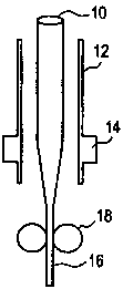
Fig. 2a is a schematic illustration of a viscously sintered extruded body in a
drawing furnace.
Fig. 2b is an illustration of a cross section of an extruded or a drawn body.
Fig. 2c is an illustration of a bundle of extruded bodies prior to drawing.
Fig. 3 is a chart showing the pass bands and band gaps of a photonic crystal.
Figs. 4 is an illustration of a cross section taken through the long axis of
the
extruded or drawn photonic crystal in which the periodic features are shown.
Fig. 5 is an illustration of a 2-D photonic crystal having a waveguide path
therethrough.
Fig. fi is an illustration of a waveguide fiber having a solid glass core and
a
photonic crystal cladding.
Fig. 7 is an illustration of a waveguide fiber having a large central channel
surrounded by a photonic crystal comprised of smaller openings or filaments.
Fig. 8 is an example of channels of different size overlapped to provide a
first
periodic structure having a first channels size embedded in a second periodic
structure having a second channel size.
Fig. 9 is a drawing of a reducing die.
CA 02339114 2001-O1-30
WO 00/06506 PCT/US99/16178
Detailed Description of the invention
The photonic crystal art is still in a rapidly developing stage in which the
fundamental shapes, properties and uses of two or three dimensional crystals
are being tested.
5 The extrusion process is distinctly suited for making a wide variety of
photonic crystals because the extrusion art:
- is mature in that processes are available for extruding a wide range of
materials and shapes;
- is capable of producing periodic structures having very small wall
thickness, a
10 high degree of open frontal area, and a high channel (cell) density as
measured in terms of number of channels (cells) per unit cross sectional area;
- can be kept free of contamination, for example, by means of coated dies and
mixers, so that the purity of extruded structures is limited only by the
purity of
the starting materials;
- is compatible with glass starting materials such as amorphous silica powder
mixed with a binder; and,
- can provide, by means of reduction extrusion, a wide range of channel
densities simply by changing the cross section area of the body produced in
the initial or reduction extruding step.
The extrusion process is documented elsewhere and so will not be set
forth in detail herein. The extrusion methods and apparatus used in the
invention described herein may be found for example in U.S. patent 3,790,654,
Bagley and U.S. patent 4,902,216, Cunningham et al. the specifications of
which are incorporated into this document by reference. This technology is
capable of extruding tens of thousands of channels simultaneously.
In an exemplary initial extrusion of a material, such as silica powder or
PyrexT'" powder, through a die, a channel density of about 62 channels per cm2
has been demonstrated. Subsequent passing of the initial extruded body
through a reduction die, which may be a funnel, can produce a channel density
of about 6200 channels per cm2. Higher channel densities are then achieved
by hot drawing the viscously sintered extruded substrate.
CA 02339114 2001-O1-30
WO 00/06506 PCT/US99/I6178
11
Referring to Fig. 9, reduction die body 78 is shown having an input
funnel 74 into which the extruded body 72 is introduced. A mechanism for
applying forward force to the extruded body, not shown, causes the extruded
body to pass through reducing section 76 and emerge as reduced body 80.
After reduction extrusion, the minimum spacing between channel
centers, assuming uniform wall thickness, is then of the order of 30 pm, a
limit
which is set by the desire that the minimum web thickness be about 10 particle
diameters. It is understood that this wall thickness can also be achieved by
extruding followed by heating and drawing. That is, the reduction step is
optional and typically is used in those cases where the drawing furnace
dimensions are a limiting factor.
To reach a feature spacing for certain applications of a photonic crystal,
in the
near infrared part of the spectrum, a spacing of about ~,/3 or 0.5 ~m is
desired.
However, the feature spacing may be larger than the sub-micron level, of the
order of several microns, and still produce useful photonic crystal
structures. In
either case the extrusion process can be used to fabricate the photonic
crystal
structure. After the structure is extruded and then, optionally, further
reduced
by passing the body through a reduction die, the resulting body is heated to
drive off the binder and then viscously sintered to produce a body which is
heated and drawn to further reduce the thickness dimension of the body and
reach the desired pitch, of the order of tenths of microns, characteristic of
an
optically active structure.
The combination of extrusion technology, with that of drawing, provides
a unique and versatile process for fabricating photonic crystals. The
extrusion
process provides a wide range of cross sectional shapes while maintaining
dimensional accuracy of the shapes. The dimensional accuracy of the drawing
process, which meets or exceeds that of extrusion, make the combination of
these two processes a powerful tool in the manufacture of photonic crystals.
The periodic array need not include channels of any kind, because the
extrusion process, e.g., a back fill or co-extrusion process, can make use of
one or more starting materials and embed a periodic array of one material
CA 02339114 2001-O1-30
WO 00/06506 PCT/US99/16178
12
within the matrix of the other. That is, the photonic crystal is a solid glass
body
which exhibits a periodic variation in dielectric constant of solid materials.
The viscously sintered or extruded body shown in Fig. 1 is a periodic
array of square channels. The body was made from an extrudate of silica
powder in a binder. The extruded body was heated to drive off the binder.
Subsequently the temperature of the body was increased to provide for viscous
sintering. The regularity of the array is noteworthy. Depending upon the final
configuration chosen for the photonic crystal, either the channels 8 or the
walls
(web) 6 of the extruded and drawn body could function as the periodic feature
of the crystal.
A schematic representation of the drawing process is shown in Fig. 2a.
The extruded, reduced, if needed, and viscously sintered body 10 is
suspended in furnace 12. The suspending means, which include means for
feeding the glass body into the furnace, are not shown but are known in the
art.
Coil 14 represents the heating element of furnace 12. The localization of the
hot zone near one end of the furnace provides a furnace temperature profile
that allows a continuous and uniform glass rod or fiber 16 to be drawn from
the
sintered body 10 by gripping means 18. Alternative gripping means are known,
including types which translate with the drawn rod or fiber 16. The extruded
and reduced body 10 may be viscously sintered during the drawing step if the
tensile strength of the unsintered body is sufficient to support the draw
tension.
As has been noted above, if the extruded body or extr tided and sintered body
has a small enough diameter, the reduction may be excluded, and drawing
begun immediately after the extrusion step. It is believed that the necessary
geometry may be extruded into a preform having a diameter not substantially
larger than about 5 cm, which is a size compatible with most draw furnaces.
In an alternative embodiment of the invention, the draw down process is
carried out in two steps. The viscously sintered body is first drawn into a
rod or
fiber which is then overclad and drawn to a fiber, which typically has a clad
diameter of the order of 100's of microns and a photonic crystal core diameter
of 10's of microns. This process is expected to be useful in obtaining
structures having very high channel density.
CA 02339114 2001-O1-30
WO 00/06506 PCT/US99/16178
13
The cross section shown in Fig. 2b represents an extruded channeled body, an
extruded and reduced channeled body, or an extruded, reduced and drawn
channeled body. The channels are shown as periodic array 22 which are
formed in the glass 20.
It will be understood that the structure of Fig. 2b may be formed such
that the periodic array 22 is an array of glass filament ends, in which the
dielectric constant of glass array 22 is different from that of glass matrix
20.
Thus in describing a body having channels, applicants at the same time are
describing a body comprising a first and a second glass one embedded in the
other to form a periodic array of dielectric constant differences.
An important feature of the invention is the capability of substantially
preserving the extruded shape through subsequent process steps in which a
cross section of the shape is reduced in size.
To produce a photonic crystal having a pre-selected periodicity,
illustrated as surfaces 28 in Fig. Zc, and a larger surface area, a plurality
of
extruded or extruded and reduced channeled bodies, 26 in Fig. 2c, may be
bundled, using for example a surrounding tube 24 as a drawing aid, and drawn
as a unit. As.an alternative, channeled bodies having different periodicity
may
be bundled as shown in Fig. 2c and drawn as a unit, thereby producing a set of
photonic crystals having different band pass and band gap wavelengths. The
units so drawn may be several interleaved periodicities and have different
crystal structures or be comprised of misaligned crystals. Some of the
channeled bodies may have a periodicity intentionally made to be random.
The need for data in this field fits well with the versatility of the process
combinations described and disclosed herein.
Fig. 3 illustrates the relative sizes of the pass band and band gap
wavelength ranges. The frequency, in relative units, of the light is plotted
on
the y-axis versus the light wave vector on the x-axis, in relative units. The
first,
second, and third band gaps, 30, 32 and 34, respectively, are shown as
frequencies within the dashed lines. The allowed or propagated frequency
bands are above and below each of the gaps.
CA 02339114 2001-O1-30
WO 00/06506 PCT/US99/16178
14
An embodiment of a photonic crystal made using the method described
herein is shown in Fig. 4. The extrusion steps and subsequent sintering and
drawing of the extruded body produces an elongated rod or fiber 40 having a
periodic array of channels 38 extending through matrix glass 36.
Another embodiment of a photonic crystal made using the method
disclosed, is illustrated in Fig. 5. Here the periodic pattern of channels has
been altered to include two intersecting line defects 44 and 46. The width of
the line defect is chosen such that the intersecting line defects serve as
waveguide paths for light having a wavelength in the band gap of the crystal.
The photonic crystal guides the light, even around a sharp bend, without
producing any excess loss. Arrows 48 and 50 indicate a direction of travel of
the light. The waveguide path is formed in the crystal in the first extruding
step
and maintained therein through the heating and drawing step. Note that the
direction of light travel in this embodiment is at a non-zero angle with
respect to
95 the photonic crystal centerline, so that the light enters and exits from a
side of
the photonic crystal rod or fiber.
A waveguide having a photonic crystal clad layer is illustrated in Fig. 6.
A solid glass core 56 is surrounded by photonic crystal 52. The circles 54
indicate the positions of material or the channels which form the periodic
array
of dielectric constants. This waveguide structure, which is readily made by
the
novel method described herein, has been found (see reference above) to
provide an unusually wide range of wavelengths over which the waveguide
propagates a single mode.
A contemplated waveguide structure which is thought to be of interest is
illustrated in Fig.7. In this case, the core region 58 is a hollow cylinder in
the
photonic crystal matrix glass 62. As before the circles 60 represent the
periodic dielectric constant array embedded in glass 62. Circles 60 represent
either channels or glass filaments extending along the waveguide length.
As an example of the versatility of the novel process, Fig. 8 shows two
sets of periodic features 66 and 64 embedded in matrix glass 70. The sets of
circles and dots are each representative of a periodic array. The size or
periodicity of the feature can be selected to provide a particular band gap.
CA 02339114 2001-O1-30
WO 00/0650b PCT/US99/16178
Here again the extrusion technology is well suited to making such overlapping
or interwoven structures.
Although various embodiments of the invention have hereinabove been
disclosed and described, the invention is nonetheless limited only by the
5 following claims.