Note : Les descriptions sont présentées dans la langue officielle dans laquelle elles ont été soumises.
CA 02343885 2001-03-13
',
GR 98 P 2971
Description
Surface acoustic wave arrangement having at least two
surface acoustic wave structures
The invention relates to surface acoustic wave
arrangements having at least two aurface acoustic wave
structures which are adjacent in the main wave
propagation direction and in which the period of the
fingers in the first surface acoustic wave structure is
different to that of the fingers in the second surface
acoustic wave structure, and/or they are shifted in
phase with respect to one another.
In addition to the normal propagation losses,
broadband losses occur, due to partial conversion of
the surface acoustic wave into volume waves, at the
junction between two surface acoustic wave structures
which are different or are phase-shifted with respect
to one another. The conversion losses in this case
increase as the metallization height increases. This is
described, for example, in an article by Yasuo Ebata,
"SUPPRESSION OF BULK-SCATTERING LOSS IN SAW RESONATOR
WITH QUASI-CONSTANT ACOUSTIC REFLECTION PERIODICITY" in
Ultrasonics Symposium 1988, pp. 91-96.
This situation occurs, in particular, when
- the two lattice elements (surface acoustic wave
structures) differ in terms of period length,
metallization ratio and/or layer thickness, or
- the distance between the two surface acoustic wave
structures is chosen such that the two lattice
elements are phase-shifted with respect to one
another.
With many filter techniques, such discrepancies
from perfect periodicity are essential for the method
of operation of the filter (for example: DMS filter).
It has thus been proposed, in DE 42 12 517, that the
junction between the two surface acoustic wave
structures be designed to be quasi-;periodic. However,
CA 02343885 2001-03-13
h
GR 98 P 2971 - 2 -
this technique has been found to be sufficiently
successful only if the relative difference between the
speeds of the surface acoustic wave and the interfering
volume wave is considerably greater than the relative
useful bandwidth of the filter, as is the case, for
example, with narrowband IF filters on quartz. This is
the only situation where the interference of the
parasitic volume wave with the transfer function is
outside the pass band of the filter and thus does not
interfere with the filter response:
However, low-loss filters having a broader
bandwidth are required for telecommunications networks
based on the EGSM Standard or for 1?CS/PCN.
DMS filters (double mode aurface acoustic wave
filters) are frequently used as low-loss, broadband
filters with high selectivity for RF purposes, for
example on a 42° red YX-LiTa03 substrate or on a 36°
red YX-LiTa03.
One example of a simple single-track DMS filter
is illustrated schematically in figure 1. This filter
in this case comprises a track having input transducers
El and E2, which are arranged between two reflectors R1
and R2, and the output transducer A. The connections
for the input and output transducers can also be
interchanged, with A then representing the input
transducer, and El, E2 the output= transducers. It is
also possible to connect the output transducer, or else
the output transducers, of this on.e track to the input
transducer, or input transducers, of a second, parallel
track. This allows the selectivity of the filter to be
increased.
DMS filters have two separate resonant
frequencies within one acoustic track, which define a
transmission band. The left-hand edge of the
transmission band is governed by the lattice period,
while the right-hand edge comes about due to the
resonance between two mutually shifted surface acoustic
wave structures (input and output transducers). In
iE
" CA 02343885 2001-03-13
' _,~.3
GR 98 P 2971 - 2a -
comparison to a periodic lattice, these two structures
have been shifted through a Ox of .approximately ~,/4
' CA 02343885 2001-03-13
't ~ ~
GR 98 P 2971 - 3 -
with respect to one another. The distance ~x in this
case relates to the finger centers of adjacent
(electrode) fingers of the surface acoustic wave
structures. In practice, one of the two end fingers is
preferably broadened by approximately ~,/4, as is shown
in figure 1 for the output transducer A at the junction
to the two input transducers E l and E2. This is done in
order to fill the gap between the two structures with a
metallized surface, since any surface leakage wave is
carried better under a metallized surface.
This results in a structure having a greatly
broadened finger, which has a considerably greater
local lattice period p (defined by the distance between
the center points of the two free surfaces to the left
and right of the finger) than the other fingers. This
represents a considerable disturbance with the periodic
lattice. Figure 2 shows, schematically, the profile of
the finger period p in the region of the junction
between two such transducer structures (surface
acoustic wave structures) plotted against the position
coordinate x, the propagation direction of tha surface
acoustic waves.
In mobile radio systems (for example GSM,
nominal bandwidth 25 MHz) which have been used until
now, it has admittedly been possible to identify the
acoustic losses in the form of volume wave emission at
the structure junctions, but this has not been so
severely pronounced for the provision of low-loss
filters to be possible. However, broader bandwidths
will be used in future mobile radio systems, in order
to provide more channels (for example EGSM, nominal
bandwidth 35 MHz).
Normally, the bandwidth o f surface acoustic
wave filters is increased by increasing the
metallization layer thicknesses and reducing the number
of fingers. Both measures increase the losses at the
junctions between the structures. In practice, these
losses result in a reduction in the Q-factor of
CA 02343885 2001-03-13
GR 98 P 2971 - 3a
the transducer/transducer resonance, which defines the
right-hand
' CA 02343885 2001-03-13
s
GR 98 P 2971 -
band edge, and thus in a reduction in the upper pass
band range.
Particularly in the case of EGSM filters, the
influence of the losses is so great that the reduction
in the upper pass band must be compensated for by means
of additional, external matching elements. The external
matching can admittedly reduce the amount of ripple in
the pass band, but a significant remaining disadvantage
is the increased insertion loss of such filters
resulting from the losses at the junctions. The
specification required for EGSM, for example, can also
only partially be satisfied. External matching networks
are, furthermore, always associated with additional
costs, weight, surface area on the circuit and
production complexity, and are i~hus undesirable for
most users.
The object of the present invention is thus to
provide low-loss broadband filters which avoid the
disadvantages mentioned above.
According to the invention, this object is
achieved by a surface acoustic wave arrangement as
claimed in claim 1. Further :refinements of the
invention are described in the dependent claims.
The invention results in a reduction in the
transmission losses of the filter, which is evident in
the improved insertion loss and, in particular, in the
upper half of the pass band. The useful bandwidth is
thus increased, and there is no need for any external
matching networks.
When designing broadband, low-loss surface
acoustic wave filters (for example RF filters for EGSM
or PCS/PCN on 42° red YX-LiTa03), the inventors found
that additional losses, in the form of conversion to
volume waves, also occur in a quasi-periodic lattice if
the local period at the junction is greater than in the
two structures on both sides of the junction. In
contrast to a hard transition,
' CA 02343885 2001-03-13
o
GR 98 P 2971
with an abruptly increased finger period, this
conversion does not, however, occur below a
characteristic onset frequency, which is inversely
proportional to the local period of the lattice.
The losses at the junctions between surface
acoustic wave structures with a different phase and/or
a different finger period are thus considerably
reduced, or entirely avoided, in that, according to the
invention, a finger period which is less than the
finger period of the adjacent surface acoustic wave
structures is used at the junction points. This results
in the onset frequency for volumes wave emission being
above the desired transmission band of the filter. The
junction between the surface acoustic wave structures
is quasi-periodic, that is to say a quasi-periodic
structure is formed in the region of the wave junction
between two surface acoustic wave structures, which
quasi-periodic structure forms a continuous transition
between the finger period p and/or the phase of the
first surface acoustic wave structure in that of the
second surface acoustic wave structure.
Depending on the extent of the discontinuity at
the junction, a quasi-periodic junction region is
formed having a sufficiently large number of fingers. A
total of 3-4 fingers at the ends of each surface
acoustic wave structure has been found to be sufficient
to suppress the losses even for very severe
discontinuities. The junction region should not
necessarily be chosen to be greater than is required to
avoid losses since, otherwise, this will have a
negative effect on the transmission response of the
filter.
The desired junction according to the invention
is achieved if the finger period of the first surface
acoustic wave structure initially decreases
continuously in the junction region and finally rises
continuously again until the finger period of the
second surface acoustic wave structure is reached.
' CA 02343885 2001-03-13
a
GR 98 P 2971 -
For the purposes of the invention, the term
surface acoustic wave structure covers both
interdigital transducers and reflectors. Junctions may
therefore occur, and be designed according to the
invention, not only between two interdigital
transducers, but also between an interdigital
transducer and a reflector; and between two reflectors.
The invention can thus advantageously be used, in
particular, for DMS filters and single-port resonators.
In the latter, the reflectors have a different
(greater) finger period than the interdigital
transducer.
The finger width and the finger spacing are
reduced continuously in order to reduce the finger
period in the junction region.
The choice of a metallization ratio r~ (r~ = ratio
of the metallized surface to the unmetallized surface
area within one period of the surface acoustic wave
structure) between 0.7 and 0.8 reduces the speed of the
surface leakage wave, as a result of which the
separation between the onset frequency for volume wave
conversion and the pass band is further increased. This
therefore also reduces the influence of volume wave
losses.
Reduced transmission losses are likewise
achieved if the reflectors of the surface acoustic wave
arrangement are connected to ground, since this results
in a considerable reduction in the lossy exchange of
charge within the reflector.
The invention will be explained in more detail
in the following text, with reference to exemplary
embodiments and the five associated figures, in which:
Figure 1 shows a known single-track DMS filter.
Figure 2 shows the profile of the finger period of the
known filter (see figure 1) along the
position coordinate.
CA 02343885 2001-03-13
D
GR 98 P 2971 - 7 -
Figure 3 shows the profile of the finger period for a
surface acoustic wave arrangement according
to the invention.
Figure 4a shows two surface acoustic wave structures
having a hard transition,, in which,
Figure 4b a surface acoustic wave arrangement having a
junction according to the invention between
two surface acoustic wave structures is shown
for comparison.
Figure 5 shows a comparison of the pass characteristic
of filters according to the invention and
known filters, based on measured curves.
Figure 1 shows a known single-track DMS filter,
in which two parallel-connected input transducers E1,
E2, with an output transducer A between them, are
arranged between two reflectors R1. and R2. In and Out
denote the electrical connections for the input and
output. The finger period p, which is a measure of the
distances between the fingers, is defined in the
following text as the distance which extends from the
center of the free space between two fingers to the
center of the next free space between two adjacent
fingers. In the illustrated DMS filter, the output
transducer A is shifted with respect to the two input
transducers E1 and E2, with the finger period in each
case having a discontinuity at the E1/A and A/E2
junctions between two mutually shifted transducers.
Figure 2 shows the profile of the finger period
for these transducers in the region of the junction
between transducer El and the transducer A. The shift
of the two transducers with respect to one another is
expressed in an abruptly rising finger period which
then falls, likewise abruptly, once again to a constant
value. The same hard transition can be seen between the
CA 02343885 2001-03-13
GR 98 P 2971 - 7a
two transducers A and E2 which have been shifted with
respect to one another. The two outer end fingers of
the transducer A have been broadened in order to fill
the gap between the two structures with a metallized
T
CA 02343885 2001-03-13
GR 98 P 2971 - 8 -
surface. The disadvantages which result from such a
discontinuity in the profile of the finger period at
the junction between two surface acoustic wave
structures (in this case two transducers) have already
been explained in the introduction.
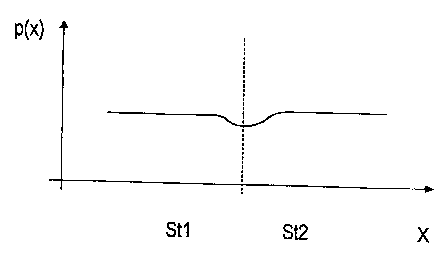
Figure 3 shows the profile of the finger period
p for a surface acoustic wave arrangement according to
the invention, in the region of the junction between a
first surface acoustic wave structure Stl and a second
surface acoustic wave structure Si~2. The finger period
p varies continuously in the region of the junction,
where it also has a lower value than in either of the
two structures Stl or St2. Outside the junction region,
that is to say within the two structures St r and St2,
the finger period assumes a constant value, which may
differ from one surface acoustic wave structure to
another surface acoustic wave structure. The surface
acoustic wave structure may in this case be an
interdigital transducer or a reflector, in which case
the junction may occur between a transducer and a
transducer, or between a transducez- and a reflector.
Figure 4 uses an exemplary embodiment to show
how the junction between two mutually shifted surface
acoustic wave structures Stl and St2 may be configured
according to the invention. For comparison, figure 4a
shows a known hard transition, as has already been
described with reference to figure 1. In this case, one
of the two boundary fingers has been broadened.
Figure 4b shows the junction designed according to the
invention. The finger period p ha.s in this case been
reduced continuously over the last three fingers of the
structure Stl, and likewise rises continuously once
again over the outermost three fingers in the adjacent
structure St2. This arrangement considerably reduces
the scattering losses at the junction between the two
structures, in comparison to a known arrangement with a
hard transition.
. ° CA 02343885 2001-03-13
a
GR 98 P 2971 - ga -
Furthermore, a junction designed according to
the invention and, for example, as shown in figure 4b,
is simple to manufacture sinca neither the
CA 02343885 2001-03-13
n 1
GR 98 P 2971 _ g _
finger widths nor the finger spacings differ too
severely from "normal" finger widths and finger
spacings.
Figure 5 shows the trap:>mission curves for
three surface acoustic wave filters which have surface
acoustic wave structures that have been shifted with
respect to one another. The DMS filter illustrated in
figure 1 is used as an example, whose transmission
response is shown by the transmission curve 1 in figure
5. The transmission curve 2 is obtained for a DMS
filter as shown in figure 1, but having a continuous
finger period profile. In this structure, the finger at
the end is not broadened, but the greater separation
between the two structures on both sides of the
junction is distributed over the respective outermost
three fingers, so that a locally increased finger
period occurs at the junction. As can clearly be seen
from the measured curve 2, a DMS filter designed in
this way has an even worse transmission response than
the filter shown in figure 1. The transmission curve 3,
on the other hand, was measured with a DMS filter
designed according to the invents.on, in which the
finger period in the region of the junction of the two
mutually shifted transducers (surface acoustic wave
structures) has been reduced, with an additional finger
being inserted, in comparison to the SAtnl filter which
is known from figure 1. In this case, both the finger
width and the finger spacing decrease continuously
toward the junction, in both transducers. As figure 5
shows, such a filter designed according to the
invention has a better transmission response, which is
indicated by reduced attenuation and a more uniform
transmission curve. The reduced attenuation,
particularly in the region of the right-hand edge of
the transmission curve, is achieved by the reduced
scattering losses in the region of the junction.
Further parameters for designing DMS filters
are specified as an exemplary embodiment in the
CA 02343885 2001-03-13
t T
GR 98 P 2971 - 9a -
following text, these being suitable for the EGSM
system which has a nominal bandwidth of 35 MHz at a
mid-frequency of 942.5 MHz.
° CA 02343885 2001-03-13
a r
GR 98 P 2971 - 10 -
Lithium tantalite LiTa03 with a 42° red YX
crystal cut is used as the substrate. The metallization
for the surface acoustic wave structures is applied
with a thickness which amounts to 9 to 11 percent of
the associated wavelength, for example 420 nm. This
provides the required bandwidth of 35 MHz. The
right-hand flank of the transmission curve of the
filter, which is a result of the resonance between two
transducers shifted through a value ~x with respect to
one another, can be said to cc>mply with the EGSM
Specifications by selecting ~x - (0.25 ~ 0.05)x,. The
quasi-periodic transition of the finger period between
the two shifted transducers can b~e distributed over a
total of five to eight fingers. The total number of
electrode fingers in transducer ~~1 (see figure 1) is
preferably chosen to be in the range from 27 to 35, and
the total number of fingers in the transducers E1 and
E2 to be in the range from 20 to 24. This results in a
filter which is optimized in terms of ripple and flank
gradient.
The selectivity required f:or EGSM is obtained
with a filter having two tracks whose junction is
designed according to the invention. The aperture is
chosen to be between 50 x ~, and 70 x ~,, in order to
obtain input and output impedances of 5052:
The entire filter with a surface acoustic wave
arrangement according to the invention may also be used
in embodiments which can be operated symmetric-
ally/asymmetrically. This means, inter alia, a filter
in which an asymmetric signal is present at the input
or at the output, that is to say in which one of the
two connections is carrying a signal, while the other
is connected to ground. At the other end of the filter,
a symmetrical signal is present at the two connections,
which has the same absolute amplitude at both
connections, but with the opposite mathematical sign,
or a phase difference of 180°.
CA 02343885 2001-03-13
fi
GR 98 P 2971 - l0a -
A further application of the invention is in
DMS filters which can. be operated
symmetrically/asymmetrically and in which the input and
CA 02343885 2001-03-13
GR 98 P 2971 - 11 -
output impedance differ. The inputs or output impedance
can be adjusted by weighting or by vertical or
horizontal splitting of the transducers into transducer
element structures, as is proposed, for example, in the
two prior German Patent Applications 197 24 258.8 and
197 24 259.6.
It is also possible for t:he distances between
the central interdigital transducer (A) and the two
outer interdigital transducers (E1, E2) to be of
different magnitude.
A further refinement relates to a filter which
is in the form of a two-track arrangement, with the
finger periods p of the reflectors (R) in the two
tracks being of different magnitude.
The invention can likewise be used in a
resonator filter in which the junction between a
mutually shifted transducer and reflector is designed
according to the invention. For example, a reactance
filter comprising a number of single-port resonators
connected in series and/or in parallel and having a
junction between the different finger periods (p) of
the interdigital transducer and reflector can be formed
in at least one single-port resonator..