Note : Les descriptions sont présentées dans la langue officielle dans laquelle elles ont été soumises.
CA 02388039 2009-12-02
Improved Floating, Balanced Output Circuit
Field of the Disclosure
The present application relates to a floating, balanced output circuits, and
more
specifically to an improved floating, balanced output circuit that maintains
control of the
common-mode output current in both output legs of the circuit even when the
differential
voltage output is clipped and the circuit is driving a ground-referred load.
Background of the Disclosure
Professional audio equipment often employs electronically-balanced output
circuits intended to mimic the behavior of output transformers as closely as
possible.
Such circuits are designed to accept a single-ended input voltage and to
produce a
differential output voltage with a low differential output impedance. They are
further
designed to possess a substantially higher common-mode output impedance
(common-mode output impedance being defined as the impedance from either leg
of the
differential output to the ground or reference potential). This allows the
differential
output voltage to "float" with the common-mode voltage of the load, thus
allowing the
circuit to properly drive both balanced and ground-referred loads. This
behavior is
similar to that of an output transformer, wherein the differential output
impedance is
determined by the source impedance driving the primary reflected to the
secondary
(output) winding, while the impedance from either leg of the secondary winding
to
ground is quite high, being determined primarily by the stray capacitance from
the
secondary winding to ground. A consequence of this arrangement is that the
output
currents exiting the two legs of the balanced output are substantially equal
in magnitude
and opposite in polarity regardless of the load configuration.
1
CA 02388039 2002-04-17
WO 01/35526 PCT/US00/41941
A widely used circuit described in 1980 (T. Hay, "Differential Technology in
Recording Consoles and the Impact of Transformerless Circuitry on Grounding
Technique." Presented at the 67th Convention of the Audio Engineering Society,
Journal
of Audio Engineering Society (Abstracts), vol. 28, p.924 (Dec. 1980)) is shown
in Figure
1. It accepts a single-ended input voltage vin with respect to ground at
terminal IN. It
produces a differential output voltage (equal to twice the input voltage)
between nodes
OUT+ and OUT-. This circuit accomplishes the desired goals with respect to
differential
and common-mode output impedances. Under normal operation, the differential
output
impedance is substantially determined by the sum of output resistances Rai and
R02, as
negative feedback around the operational amplifiers OAI and OA2 substantially
reduces
their internal closed-loop output impedances. Rol and RO2 are typically
between 10 and
100 ohms in order to keep the differential output impedance relatively low.
The
common-mode output impedance is quite high, and can be infinite if the ratios
of the
resistances labeled R and 2R in the schematic are precisely maintained. It
should be
noted that mismatches in these resistor ratios can either reduce the common-
mode output
impedance if the mismatches are in one direction, or can lead to instability
if they are in
the other direction. This requirement for precise resistor-ratio matching is a
drawback to
this circuit.
It should be clear that the common-mode behavior of the circuit of Figure 1 is
governed by both opamps, OA1 and OA2. When driving a single-ended load, as in
Figure 2, the combined common-mode feedback forces the output currents to be
equal
and opposite (assuming exact resistor ratios around the opamps). This behavior
is one of
the most desirable properties of such circuits. However, if an input signal is
applied to
terminal IN that causes the output signal at the ungrounded output (in this
case, OUT+),
to exceed the maximum permitted by the power supply voltage, both the
differential and
common-mode feedback loops are broken. As is expected, the differential output
voltage
waveform at the OUT+ output would be "clipped" at the opamp's maximum output
voltage. Its output current will be the output voltage divided by the load
resistance.
What is not as obvious is that, while clipping is occurring, the output
current of the
grounded OUT- output will be quite high, typically limited only by any
protective
current limiting circuit in the opamp, or by the maximum opamp output voltage
divided
2
CA 02388039 2002-04-17
WO 01/35526 PCT/US00/41941
by the value of the 10-to-100 ohm output resistor. This current must flow
through an
indeterminate path through the ground structure of the load device to return
to the output
stage, which can lead to disturbances on the audio waveform that are more
audible than
simple clipping.
An alternative approach to a floating balanced output circuit was described in
1990 by Chris Strahm in US Patent 4,979,218. Strahm's circuit includes
separate
feedback loops for differential and common-mode output signals. The
differential loop
is configured to force the differential output voltage to substantially equal
the input
voltage multiplied by some desired gain, and the common-mode feedback loop is
configured to force the two output terminal currents to be equal and opposite.
This at
least opens up the possibility of preventing the clipping behavior and the
audio waveform
disturbances described above. Also, as described in the Strahm patent, precise
resistor
ratios are not necessary to maintain stability of the circuit.
Although not mentioned in the Strahm patent, in order to prevent a grounded
output of such a circuit from going into current limiting when the active
output is driven
into voltage clipping, the common-mode feedback loop must remain active even
though
the differential feedback loop is disabled. In fact, the integrated circuit
device
manufactured by the assignee (Audio Teknology Inc.) based on the Strahm patent
is
implemented in a way that does not preserve the functionality of the common-
mode
feedback loop when the differential feedback loop is broken due to voltage
clipping into
a grounded load. As shown in Figure 3, a differential pair of transistors, Q,
and Q2,
accept the input signal and the differential feedback signal. Transistor Q3
provides the
tail current Ita;, for the differential pair. Q3 is controlled by the common-
mode feedback
signal. In this case, the common-mode feedback signal is derived by sensing
the sum of
the output currents from the device, as described in the Strahm patent. Thus,
the
common-mode output voltage is adjusted via feedback through Ita;, until the
two device
output currents sum to nearly zero, and, are thus nearly equal and opposite.
When
voltage clipping occurs at either amplifier output, one of Q, or Q2 will
saturate while the
other will be cut off. If the circuit is driving a ground-referred load from
the output
amplifier that is driven by the cutoff transistor, then there is no way for Q3
to affect the
output voltage and common-mode feedback is also disabled. Without common-mode
3
CA 02388039 2009-12-02
feedback to maintain control over the output currents, the grounded output
amplifier conducts
as much current as permitted by other aspects of the amplifier design, such as
protective current
limiting.
In accordance with one aspect of the present invention, there is provided a
floating,
balanced output circuit for providing a differential output voltage in
response to an input voltage,
with a relatively low differential output impedance and a relatively high
common-mode output
impedance, comprising: a first transconductance amplifier section for
providing a differential pair
of output currents in response to the input voltage, the currents being
substantially equal in
magnitude and opposite in polarity; an intermediate section connected so as to
generate an
intermediate differential voltage in response to the pair of output currents
of the first
transconductance amplifier; an output section for generating the differential
output voltage in
response to the intermediate differential voltage; a differential feedback
loop configuration
connected around the first transconductance amplifier section and the
intermediate section so as
to provide differential negative feedback; and a common-mode feedback loop
configuration
comprising a second transconductance amplifier section connected around the
intermediate
section so as to respectively add a pair of substantially matched output
currents to the output
currents of a first transconductance amplifier stage in response to a common
mode current;
wherein the first and second transconductance amplifiers are designed so that
the common mode
feedback loop configuration remains active when the differential loop
configuration has been
disabled due to clipping when the input voltage exceeds a predefined level.
In accordance with another aspect of the present invention, there is provided
a floating,
balanced output circuit for providing a differential output voltage in
response to an input voltage,
with a relatively low differential output impedance and a relatively high
common-mode output
impedance, comprising: a main current path including a first transconductance
amplifier section
for providing a differential pair of output currents in response to the input
voltage, the currents
being substantially equal in magnitude and opposite in polarity, and a
subsequent section
connected so as to generate an output signal in response to the pair of output
currents of the first
transconductance amplifier; a differential feedback loop configuration
connected around the first
transconductance amplifier section so as to provide differential negative
feedback; and a
common-mode feedback loop configuration comprising a second transconductance
amplifier
section connected around the subsequent section so as to respectively add a
pair of substantially
matched output currents to the output currents of a first transconductance
amplifier stage in
response to the output signal; wherein the first and second transconductance
amplifiers are
4
CA 02388039 2009-12-02
designed so that the common mode feedback loop configuration remains active
when the
differential loop configuration has been disabled due to clipping when the
input voltage exceeds
a predefined level.
In accordance with a further aspect of the present invention, there is
provided a method
of configuring a floating, balanced output circuit so as to provide a
differential output voltage in
response to an input voltage, with a relatively low differential output
impedance and a relatively
high common-mode output impedance, comprising: configuring and connecting the
following
components: a main current path including a first transconductance amplifier
section for
providing a differential pair of output currents in response to the input
voltage, the currents being
substantially equal in magnitude and opposite in polarity, and a subsequent
section connected so
as to generate an output signal in response to the pair of output currents of
the first
transconductance amplifier; a differential feedback loop configuration
connected around the first
transconductance amplifier section so as to provide differential negative
feedback; and a
common-mode feedback loop configuration comprising a second transconductance
amplifier
section connected around the subsequent section so as to respectively add a
pair of substantially
matched output currents to the output currents of a first transconductance
amplifier stage in
response to the output signal; wherein the first and second transconductance
amplifiers are
designed so that the common mode feedback loop configuration remains active
when the
differential loop configuration has been disabled due to clipping when the
input voltage exceeds
a predefined level.
Brief Description of the Drawings
Figure 1 is a schematic drawing of a prior art circuit that uses positive and
negative
feedback to emulate a floating voltage source;
Figure 2 shows a schematic drawing of the prior art circuit of Figure 1
connected to drive
a single ended load;
Figure 3 shows a schematic drawing of a prior art circuit for implementing a
common
mode feedback loop;
Figure 4 shows a schematic drawing of an improved circuit that uses separate
differential
and common-mode feedback loops to emulate a floating voltage source and
controls the output
common-mode current under clipping conditions while driving a ground-referred
load;
Figure 5 shows a schematic drawing of the preferred transconductance
amplifiers used
in the Figure 4 circuit;
4a
CA 02388039 2009-12-02
Figure 6 shows a schematic drawing of the differential-input, dual-output
transconductance amplifier shown in Figure 5 modified to include an additional
gain stage;
Figure 7 shows a schematic drawing illustrates a further modification to
minimize output
common-mode voltage; and
Figure 8 shows a schematic drawing illustrates another modification to
minimize output
common-mode voltage.
Detailed Description of the Drawings
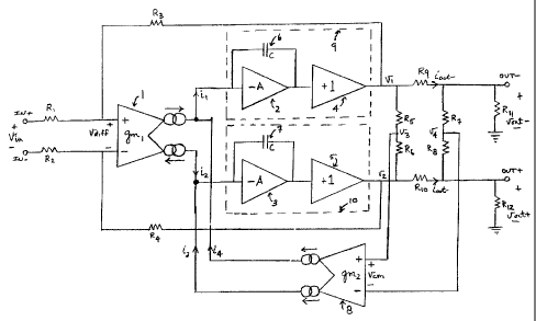
Figure 4 shows a schematic drawing of one embodiment of an improved circuit
that uses
separate differential and common-mode feedback loops to emulate a floating
4b
CA 02388039 2002-04-17
WO 01/35526 PCT/US00/41941
voltage source and controls the output common-mode current under clipping
conditions
while driving a ground-referred load. As shown, transconductance amplifier 1
is a circuit
that accepts a differential input voltage and delivers as its outputs a pair
of differential
output currents such that:
(1) ii = 42 = gml = vdiff
This transconductance amplifier, along with identical inverting high-gain
voltage
amplifiers 2 and 3, identical buffer amplifiers 4 and 5, and identical
compensation
capacitors 6 and 7 form a two-stage fully-differential operational amplifier.
Resistors R,
and R2 are connected from the input voltage terminals IN+ and IN-,
respectively, to the
non-inverting and inverting terminals of transconductance amplifier 1,
respectively.
Resistors R3 and R4 are connected from the outputs of buffer amplifiers 4 and
5,
respectively, to the non-inverting and inverting inputs of transconductance
amplifier 1,
respectively, to provide differential negative feedback. As long as the
forward gain
provided by transconductance amplifier 1 and voltage amplifiers 2 and 3 is
large
compared to the desired closed loop gain, then the differential closed loop
gain Acid will
be substantially:
(2) Acrd = your+ - vOUr- - R3 + R4
Vin R, + R2
Preferably, R, = R2 and R3 = R4, so that the differential closed loop gain
will be:
(3) Acid = RR4
1
In a preferred embodiment, R, = R2 = 5 kQ2 and R3 = R4 = 10 kQ. It should be
noted that
either terminal IN+ or IN- can be grounded, and the input signal connected in
a
single-ended fashion, with no loss of functionality.
Transconductance amplifier 8 is a circuit that accepts a differential input
voltage
and delivers as its outputs a pair of matched output currents i3 and i4 such
that:
(4) i3 = i4 = 9m2 = vcm
These output currents i3 and i4 respectively sum with the output currents i2
and it of
transconductance amplifier 1. Note that the output currents i3 and i4 from
5
CA 02388039 2002-04-17
WO 01/35526 PCTIUSOO/41941
transconductance amplifier 8 will cause both output voltages (V., and Vout_)
to move in
the same direction, while the output currents it and i2 from transconductance
amplifier 1
will cause the two output voltages (vout+ and vout- ) to move in opposite
directions.
Resistors R9 and R10 are used to sense the individual output currents, and
preferably are of equal value between about 10 and about 100 ohms in order to
maintain
low differential output impedance, although the values can be outside this
range.
Resistors Rõ and R12 serve to establish a minimum common-mode load for the
circuit,
and are preferably between about 1 kQ and about 100 kQ, although the values
can be
outside this range. Resistors R5 through R$ form a bridge used to sense the
common-mode output current. Preferably, R5 = R6 and R7 = R8. In this case the
voltage
v3 at the junction of R5 and R6 will be:
(5) v3 = Vl + V2
2
and the voltage v4 at the junction of R7 and R8 will be:
(6) V4 = vou,+ + V out-
2
Noting that the currents through R9 and R10 are:
(7) iout+ = y2 - V out+ and
Rio
(o
_ V1 - Vout-
(8) foul- = R
9
the input voltage to transconductance amplifier 8 will be:
(9) vcm = lour- ' R9 + ioul+ ' Rio
2
Assuming that R9 and R10 are equal, this voltage is:
(10) vcm = (iou,+ + iou,- R9
2
which is proportional to the common-mode output current,
6
CA 02388039 2002-04-17
WO 01/35526 PCT/US00/41941
(1 1) `lout+ + lour )
2
The large gain provided by the combination of transconductance amplifier 8 and
voltage
amplifiers 2 and 3 will tend to minimize the differential voltage at the
transconductance
amplifier's inputs via negative feedback. This will then tend to minimize the
common-mode output current, leaving only differential (equal and opposite)
currents.
Both transconductance amplifiers must be designed to have a maximum possible
output current that is achieved when the input voltage exceeds a predefined
level. (This
is a natural consequence of the preferred implementations, as will be
illustrated below).
In order to ensure that the common mode feedback loop will remain active when
the
differential loop has been disabled due to clipping, the maximum output
currents from
transconductance amplifier 8 must be made greater than the maximum output
currents
from transconductance amplifier 1. As an example, assume that R11 is a short
circuit,
such that R12 serves as a ground-referred load, and that the input voltage vin
is
sufficiently positive to drive v2 to the maximum possible positive voltage
allowed by the
circuit power supplies. The negative feedback path via R4 is now broken, as
the voltage
v2 no longer responds to any change in the input voltage. Under such
conditions, i, and i2
will be at their maximum possible values (in opposite directions). Current i,
will tend to
drive voltage v1 negative, and, if left unchecked, will cause a large current
to flow
through low-valued resistor R9. However, if transconductance amplifier 8 has
sufficient
output current capability to sink the maximum value of i,, then the common-
mode
feedback loop will act to minimize the common-mode output current. Under these
conditions, 4 will be substantially equal to -i,, and lout- will be
substantially equal to
-iout+.
It should be clear that output stages 9 and 10, consisting of voltage
amplifiers 2
and 3, buffer stages 4 and 5, and compensation capacitors 6 and 7 may take
many
preferred forms without departing from the scope of the invention. As an
example, when
utilizing bipolar transistors, voltage amplifiers 2 and 3 may consist of
current-source-loaded common emitter amplifiers, and buffer amplifiers 4 and 5
may
consist of complementary common-collector amplifiers. Other devices, such as
MOS
7
CA 02388039 2002-04-17
WO 01/35526 PCT/US00/41941
transistors, could also be substituted with no loss of essential
functionality. Also,
differential feedback resistors R3 and R4 could alternately be connected
directly to the
OUT+ and OUT- terminals, rather than to the outputs of buffer amplifiers 4 and
5. Such
an arrangement would result in lower differential output impedance, but would
require
more elaborate frequency compensation in order to maintain stability into
capacitive
loads.
A preferred embodiment of transconductance amplifier 1 is shown in Figure 5.
This structure comprises differential pair transistors Q, and Q2, current
sources I,, I2, and
I3 and optional equal-valued emitter degeneration resistors R13 and R14. The
differential
input to the transconductance amplifier is applied to the bases of Q, and Q2.
The
differential output currents are taken from the collectors of Q, and Q2.
Preferably, the
values of current sources I2 and I3 are each equal to one half of the value of
current source
I. In this case, the maximum current available in either direction from the
collectors of
Q1 and Q2 is equal to I1/2. The transconductance from the voltage between the
bases of
Q, and Q2 to either of the collectors of Q, or Q2 is:
(12) 1 _ 1
gõ>> - 2kT 2kT
+ R13 + R14 + 2R13
q11 q11
A preferred embodiment of transconductance amplifier 8 is also shown in Figure
5. It comprises transistors Q3, through Q8, current source I4, and optional
emitter
degeneration resistors R15 through R17. Preferably, transistor Q3 has an
emitter area twice
that of Q4 and Q5. Also, if included, the value emitter degeneration resistor
R17 is half the
value of identically- valued resistors R15 and R16. Thus, with no differential
voltage
applied between the base of transistor Q3 and the common bases of transistors
of Q4 and
Q5, Q3 will operate at a collector current equal to I4/2, and transistors Q4
and Q5 will each
operate at a collector current equal to I4/4. Similarly, transistor Q6 has an
emitter area
twice that of transistors Q7 and Q8. Thus, ignoring base currents, the
collector current of
Q6 will be mirrored to the collectors of Q7 and Q8 with a gain of 0.5, such
that each will
operate at a collector current equal to one half of Q6's collector current.
The differential
input voltage to transconductance amplifier 8 is applied between the base of
transistor Q3
and the common bases of transistors Q4 and Q5. Identical output currents are
taken from
8
CA 02388039 2002-04-17
WO 01/35526 PCTIUSOO/41941
the collectors of Q7 and Q8. The transconductance from the input differential
voltage to
either of the identical current outputs will be:
(13 1 _ 1
) S,,,z - 2kT + R15 + R16 + R17 2kT + 2R17
q14 2 q14
The maximum output current available in either direction from the collectors
of Q4 and
Q5 is equal to one half the value of current source I4. Thus, as described
above, current
source I4 should be made greater in value than current source I, in order to
ensure that the
common-mode feedback loop will remain active after the differential feedback
loop is
disabled by clipping.
In an embodiment of the invention such as that shown in Figure 5, when the
differential feedback loop has been broken due to output voltage clipping,
either
transistors Q7 and Q8 are sinking collector currents equal to at least I,/2,
or transistors Q4
and Q5 are sourcing collector currents equal to at least I,/2. Under these
conditions, a
current imbalance equal to the value of current source I, will exist between
the collector
current of Q3 and the sum of the collector currents of Q4 and Q5. This current
imbalance
will cause an input offset voltage (in addition to that caused by random
transistor and
resistor mismatches) at the inputs of transconductance amplifier 8 equal to
I,/gm2. This
additional input offset voltage will degrade the matching of the magnitudes of
the
currents in resistors R9 and R10 under the aforementioned conditions. If this
degradation
of performance is unacceptable, an additional gain stage can be added to
transconductance amplifier 8 as illustrated in Figure 6. Differential pair
transistors Q9
and Q10, optional identical emitter degeneration transistors R18 and R19,
current mirror
transistors Q11 and Q12, and current source 15 make up a differential
amplifier with a
single-ended current output. The input voltage to transconductance amplifier 8
is applied
between the bases of Q9 and Q10. The output current from the collectors of Q12
and Q10 is
applied to the base of Q5 of the previously described differential-input, dual-
output
transconductance amplifier. The common bases of Q3 and Q4 are tied to an
appropriate
bias voltage source, preferably far enough below Vcc to ensure proper
operation of
9
CA 02388039 2002-04-17
WO 01/35526 PCT/USOO/41941
current source I4 and transistors Q3 through Q5. The dual output currents are
taken from
the collectors of Q7 and Q8 as described above. With this modification to dual-
output
transconductance amplifier 8, the additional offset voltage created between
the base of Q5
and the common bases of Q3 and Q4 when the differential feedback loop is
disabled due
to clipping is reduced by the gain of differential amplifier stage 11. This
results in very
little change in input offset voltage at the bases of Q9 and Q10.
It should be understood that the functions of the circuits above can be
implemented in different ways without departing from the scope of the
invention. For
instance, the current mirrors composed of Q6 through Q8 and Q11 through Q12
could be
any of a number of improved current mirrors known in the art such as the
Wilson current
mirror, the cascoded current mirror, or the emitter-follower-augmented current
mirror.
Additionally, each mirror could have emitter degeneration resistors added to
increase the
output impedance. Further, the differential inputs of transconductance
amplifiers 1 and 8
could have emitter follower buffers, and/or bias current cancellation
circuitry added to
minimize input bias current. As mentioned above, all of the circuits could be
implemented with a different transistor technology, such as MOS transistors.
Referring to Figure 4, there will always exist some finite input offset
voltage at
the differential inputs of transconductance amplifier 8 due to transistor and
resistor
mismatches. Such offset voltages will give rise to a common-mode offset
current
flowing in resistors R9 and R10 equal to the input offset voltage divided by
the resistance
value of R9 and R10. These currents will then be converted to a common-mode
offset
voltage across resistors R11 and R12 (and any external load resistance). As R9
and R10 are
preferably low-valued, as mentioned above, and R11 and R12 are preferably
higher valued,
a small input offset voltage at the input to transconductance amplifier 8 can
result in a
substantially larger common-mode output offset voltage at the OUT+ and OUT-
terminals. Figure 7 illustrates one preferred method to minimize this effect.
In Figure 7, capacitor C1 is inserted between the junction of resistors R7 and
R8
and the inverting input of transconductance amplifier 8. Resistor R20 is added
from the
inverting input of transconductance amplifier 8 to ground. R20 is preferably
chosen to be
large enough in value so as not to significantly load R7 and R8, preferably,
although not
CA 02388039 2002-04-17
WO 01/35526 PCTIUSOO/41941
necessarily 1 MQ or larger if R5 through R8 are all about or within a small
range of 10
kS2. C, is chosen so that the high-pass filter formed by C, and R20 has a pole
frequency
substantially lower than the operational frequencies of interest. For example,
a value of
100 nF for C, and 1 M92 for R20 will result in a pole frequencyfphp of :
1
(14) fphp = _ 2,r(100nFXIMc) 1.6Hz ,
which is well below the band of interest for audio applications. Thus, in the
audio band,
the common-mode feedback loop will minimize the output common-mode current,
forcing equal and opposite currents in R9 and R10. At DC, the common-mode
feedback
loop will tend to force the junction of R5 and R6 (and thus the output common-
mode
voltage) to the ground potential, plus or minus any input offset voltage at
transconductance amplifier 8's inputs.
One of the primary applications for floating, balanced output circuits in the
professional audio industry is to drive audio signals over cables of up to
1000 feet long.
Such cables represent a reactive load on the circuit, with resonant
frequencies that may
coincide with the unity-gain frequency of the common-mode feedback loop. Such
resonances can cause peaks in the loop transmission that will compromise the
stability of
the loop. The common-mode feedback loop can be isolated from these loading
effects
with the addition of C2, also shown in Figure 7. C2 is preferably chosen so
that the
lowpass filter that it forms with the parallel combination of R, and R8 is
substantially
higher than the operation frequencies of interest, but below the unity-gain
crossover
frequency of the common-mode feedback loop. In a preferred embodiment, with R3
through R8 all equal to about 10 kQ, C2 is equal to about 10 pF. This results
in a pole
frequency of:
(15) f = 1 3.2MHz
pip 2~(I0pFX5kS2) '
which is well above the audio band. Thus, the common-mode feedback loop will
continue to minimize the common-mode output current, while at frequencies
substantially above 3 MHz, C2 will shunt the inverting input of
transconductance
amplifier 8 to ground, isolating it from the response peaks due to resonant
loads.
11
CA 02388039 2002-04-17
WO 01/35526 PCT/USOO/41941
Figure 8 illustrates an alternative and preferred method of minimizing the
output
common-mode voltage. Capacitor C3 is inserted between the OUT- terminal and
resistor
R7. Likewise, capacitor C4 is inserted between the OUT+ terminal and resistor
R8.
Resistor R21 is added from the junction of C3 and R7 to ground, and resistor
R22 is added
from the junction of C4 and R8 to ground. In a one implementation of this
preferred
embodiment C3 and C4 are each about 10 u F, and R21 and R22 are each about 20
kQ.
Like the circuit shown in Figure 7, this circuit will minimize the common-mode
output
current in the audio band, but force the output common-mode voltage to the
ground
potential at DC. The circuit in Figure 8 will maintain a superior match
between the
output current magnitudes when driving a ground referred load compared with
the circuit
in Figure 7. This is due to the absence of any loading on R7 and R8. However,
this
comes at the expense of an additional capacitor and an additional resistor.
The embodiment and practices described in this specification have been
presented
by way of illustration rather than limitation, and various modifications,
combinations and
substitutions may be effected by those skilled in the art without departure
either in spirit
or scope from this disclosure in its broader aspects and as set forth in the
appended
claims.
12