Note : Les descriptions sont présentées dans la langue officielle dans laquelle elles ont été soumises.
CA 02392314 2002-05-22
WO 01/43232 PCT/USOO/18159
A DEVICE FOR CC UPLING RADIO FREQUENCY ENERGY
FROM VARIOUS TRANSMISSION LINES USING
VARIABLE IMPEDANCE TRANSMISSION LINES
TECHNICAL FIELD OF THE INVENTION
The present invention relates in general to radio frequencv devices and in
particular to
methods and devices for coupling radio frequency energy from transmission
lines.
BACKGROUND OF THE iNVENTION
Until this invention, coaxial taps and couplers were installed bv cutting and
connectorizing
RF cable using coaxial jumpers. The primarv disadvantage of this methodology
is the resulting
excessive loss to the host cable. Stein ee u! . U.S. Patent 5.729.184.
subsequentlv taught that a
tap can be used without connectorization: however, the Siein ei cil. invention
still caused losses of
over I dB to the host cable. Stein et ul did mention the theoretical ability
to devise taps with
coupling losses up to 20dB but did not describe a metliod for the manufacture
of such devices.
What are needed are niethods and devices embodving the ability to select the
coupling loss
and accompanying insertion loss in RF systems. In particular. such methods and
devices sliould
allow a wireless svstem not only to be tuned but also should also allow
minimization of number of
amplifiers required to RF illuminate a structure.
SiJMMARY OF THE INVFNTION
The present invention relates generallv to devices which couple
electromagnetic energy from
one electromagnetic transmission medium to one or more other transmission
media and niore
specifically to devices which couple radio frequency energy from a coaxial
cable to other coaxial
cables, antennae or other radiating devices. Further. the present invention
relates to devices which
couple radio frequency energy from a transmission medium to another
transmission or radiating
medium, with variable energy and inverse loss to the host cable.
The present invention also generally relates to a device packaging or
enclosure method
which protects the electrical components. allows for sealing against water or
other contaminant
intrusions, generally allows for connecting the device to a host cable while
preventing rotation, and
provides a means of electrically connecting the ground of one device to the
ground of another
-1-
CA 02392314 2002-05-22
WO 01/43232 PCT/USOO/18159
device. The present invention further relates to a device which can be
attached to a host cable
without the need to cut and connectorize the cable.
The principles of this invention provide not only the ability to build
couplers with coupling
losses from below 10dB to over 30dB but for the manufacture of such devices.
The construction of
these devices provides extremely low insertion losses at all values of RF
coupling losses. For
example. a coupling device of the present invention with a coupling loss of
15dB will have an
insertion loss of less than 0.BdB. A 20dB loss device will have an insertion
loss of less than 0.1dB.
Therefore, it is an object of the invention to provide means of presenting a
large impedance
to the through line cable while extracting RF energy efficiently.
It is a fiirther object of the invention to provide a technique to connect a
device to a through
line such that RF energy may be extracted at several frequencies .
Another object of the invention is to provide a method of extracting RF energy
from a
through line at several frequencies while minimizing the loss in the through
line.
It is a further object of the invention to provide a technique to extract RF
energy from a
through line at varying levels depending upon need.
Another object of the invention is to extract energy at varying levels while
causing an inverse
loss to the through line. That is the higher the coupling loss from the
through line to the output of the
object of the invention, the lower the insertion loss to the through line.
Yet another object oi'the invention is to provide a technique that allows an
output
impedance of the device to match, as close as possible, the input/output
impedance of an RF
amplifier, an antenna or another transmission line.
A further object of the invention is to provide a means of extracting RF
energy from a
through line while creating minimum intermodulation products.
It is a further object of the invention to provide a technique to extract RF
energy from a
through line while providing a minimum of loss in the through line at other
frequencies.
Another object of the invention is to provide a technique to attach the device
to a through
line and transferring the energy to the output of the device with the maximum
efficiency, that is the
minimum heating loss.
-~-
CA 02392314 2002-05-22
WO 01/43232 PCT/US00/18159
Yet another object of the invention is to provide a means of transferring
energy from the
through line to the output of the device such that the ratio of RF energy flow
will be little affected by
temperature. humidity and/or vibration.
A further object of the invention is to provide a means of inexpensively and
efficiently
asseinbling the device.
Another object of the invention is to provide a technique to manufacture or
assemble a
coupling device to respond to different frequencies, bandwidths, coupling
losses and through line
losses using preformed internal wiring.
Still another object of the invention is to accomplish the energy transfer
using a variable
impedance transmission line.
Yet another object of the invention is to provide a technique that couples
energy from a
through line to the output of the device using a single, bare conductive wire
as the variable
impedance transinission line.
Another object of the invention is to provide a nieans of controlling the
energy coupled from
a host cable to the output of the device by adjusting the distance and
configuration of the wire from
the connection to the host cable.
Yet another object of the invention is to provide a mechanical package to
contain the
electrical components.
Still another object of the invention is to provide a mechanical package that
can be sealed to
prevent water or other contaminants from degrading the electrical performance
of the device.
Another object of the invention is to provide a device which can be connected
to a host
cable by drilling only one hole and placing the device on the cable and
tightening 2 captive screws.
BRIEF DESCRIPTION OF THE DRAWINGS
For a more complete understanding of the present invention, and the advantages
thereof,
reference is now made to the following descriptions taken in conjunction with
the accompanying
drawings, in which:
FIGURE 1 A is a schematic of a coupling device according to the principles of
the invention;
FIGURE 1 B is a schematic diagram of a second coupling device according to the
principles
of the invention;
-~-
CA 02392314 2002-05-22
WO 01/43232 PCT/USOO/18159
FIGURE 1 C is a schematic diagram of a third coupling device according to the
principles of
the invention;
FIGURE 1 D is a schematic diagram of a fourth coupling device according to the
principles
of the invention;
FIGURE 2 shows an assembly and section view of the coupling device according
to the
principles of the invention;
FIGURE 3A shows an electronic assembly of an ultra low insertion loss, high
coupling loss
a coupling device such as that shown schematically in FIGURE 1 B;
FIGURE 3B shows an electronic assembly of a low insertion loss, medium
coupling loss
coupling device such as that shown schematically in FIGURE 1 B;
FIGURE 3C shows an electronic assembly of a low insertion loss, low coupling
loss
coupling device such as that shown schematicallv in FIGURE 1 C. and
FIGURE 3D shows an electronic assembly of a low insertion loss, high frequencv
coupling
device such as that shown scheniatically in FIGURE IA.
DESCRIPTION OF THE INVENTION
The principles of the present invention and their advantages are best
understood by referring
to the illustrated embodiment depicted in FIGURES 1-3 of the drawings, in
which like numbers
designate like parts.
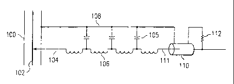
FIGURES lA and 3D respectively show a schematic and layout of a coupling
device for
coupling RF energy from a coaxial cable to a second coaxial cable, RF radiator
or RF amplifier.
Although a coaxial cable is represented. it is understood that any
transmission line can be substituted
and tapped. A hole is drilled into the host transmission line outer conductor
100 and a contact 104
(shown in FIGURE 3D at 300) is inserted to make contact with the host
transmission line center
conductor 102. The contact might be spring loaded, but it is understood that
any means of
contacting the center conductor will suffice. It is preferable that the center
conductor contact 104
(300) be insulated, but it is not necessary to meet the principles of the
invention. Insulation on the
shaft of the contact 104 (300) is provided to prevent inadvertent contact with
the outer conductor
100.
-4-
CA 02392314 2002-05-23
K~S 17 DEC 200I.
The coupler internat transmission line 106 (shown in FIGURE 3D at 326) is a
low loss wire.
The length and diameter of the wire detenaine the frequency response and to
some degree, the
coupling loss and insertion loss of the device. The transmission line wire may
be insulated to allow
longer length for lower frequencies and stiil meet the intent of the
invention.
One principle of the invention is the use of highly conductive wire. This
prevents dielectric
loss through insulation.
The wire is connected to the center conductor pin 111 (310) of an output
connector
represented by outer conductor 110 and center conductor 111 (310). It is
understood that the output
may be a hard-wired cable, a directly connected antenna, amplifier or a dummy
load. Any of these
will meet the principles of the invention.
Loss element 112 (314) is connected between the center pin 111 (310) of the
output
connector and the outer shield 110 to provide a closer impedance match to the
device connected to
the output connector. The loss element adds to the perfortnance of the
invention, but is not
required to meet the 'principles of the invention.
The configuration of FIGURES lA and 3D is used for coupling devices with
coupling
values from near -15dB to -6dB. The loss element of the internal transmission
line 106 (326) is a
low loss wire. The length and diameter of the wire determine the frequency
response and to some
degree, the coupling loss and insertion loss of the device. Parasitic
capacitors (05 are formed by
the diameter of the wire and the distance from a ground plane 108 (308) (202,
FIG. 2) shown in
FIGURE 3D. The parasitic capacitanee and the configuration of the wire
determine the center
frequency response of the device. The transmission line wire may be insulated
to allow longer
length for lower frequencies and still meet the intent of the invention. As
sho-an in FIGURE 3D,
the PC board 312 includes holes 316 for purposes that will be described in
greater detail below.
FIGURES 1B, 3A and 3B are respectively schematic and layout diagrams of an
altemate coupling
device for coupling a minimum amount of RF energy from a host cable to an
oiitput connector
while mirtirnizing the insertion loss in the host cable in accordance with the
pruiciples of the
invention.
A hole is drilled into the host transmission line outer conductor 100 and a
contact 104 (300)
is inserted to make contact with the host transmission line center conductor
102. The contact might
be spring loaded, but it is understood that any means of contacting the center
conductor will suffice.
It is preferable that the center conductor contact 102 be insulated, but it is
not necessary to meet the
principles of -the invention.
4-
AMBED %M
CA 02392314 2002-05-23
DEC 2001
The interaal transmission line 114 (306 and 320 in FIGURES 3A and 3B) is a low
loss,
non-insulated wire but may be insulated for longer lengths to accommodate
lower frequencies and
still meet the principles of the invention. The transtnission iine wire is not
to be in contact with any
dielectric except where it is connected to the ternunal points.
The length and diameter of the wire determiae the frequency respoase and to
some degree,
the coupling loss and insertion loss of the device. The parasitic capacitors
'1 15 are formed by the
diameter of the wire and the distance from a ground plane 108 (308) shown irt
FIGURE 3A. The
parasitic capacitance and the conSguration of the wire determine the center
frequency response of
the device.
One principle of the invention is the use of highly conductive wire. Tliis
prevents dielectric
loss through insulation. Still another principle of the invention is to
prevent the transmission line
wire from contacting any dielectric surface except at the point of connection.
The wire is connected to the center conductor pin 111(310) of an output
eonnector
represented by outer conductor l 10 and center conductor 111(310). It is
understood that the output
may be a hard-wired cable, a directly connected antenna, amplifier or a dummy
load. Any of these
will meet the principles of the invention.
A further principle of the invention is to not conaeet the transmission line
to the center
contact 102 (300), but using capacitive coupling, sampie the field around pin
102 as shown in detail .
in FIGURES 3A and 3B at 302 and 318. The greater the sampling, the greater the
coupling energy.
In FIGURE 1B, an element 132 represents a complex impedance, dc blocked
connection
betwcen the transmission line 114 and the pin 104 connecting the center
conductor 102 of the host
cable. This connection is fuRher shown in FIGURES 3A and 3B. As seen in
F"YG'URE 3A, the
connection can be small allowing a small amount of power to be coupled (from
20 to 30dB) or
larger per FIGURE 3B allowing coupling values of from 15 to 20dB. The high
coupling loss
causes insertion losses from 0.3 to 0.05dB.
The configuration of FIGURES IC and 3C allows a coupling device to pass
several selected
frequencies with accompanying low insertion loss at those frequencies. In
FIGURE 1 C the internal
transmission line is shown at 116 and in FIGURB 3C at 322. The lumped
impcdance 117 on
FIGURE 1 C and the coil 325 shown on FIGURE 3C allows the coupling devict to
be
D IS Ti,
__~
CA 02392314 2002-05-23
DEG 2001
configured to emphasize selected frequencies while minimizing the insertion
toss at selected
frequencies.
A further principal of this invention using the lumped impedance input, such
as shown in
FiGURES IC and 3C and the selected coupling of FIGURES 1B and 3A and 3B allows
the
designer to not only select the coupling, insertion loss, but also allow him
or ber to select the
required frequencies so that several frequencies can be seat and reeeived on
the same cable.
FIGURE ID geaerally relates to this invention with a dc blocked, complex
impedance 119
at the input of the coupled port. This allows the designer to configure the
coupling device to
customize the return loss and to some extent the frequency response. Here, the
transmission line
(intemal) is shown at 118.
FIGURE 3D generally relates to the invention for coupling devices used for
single
frequencies at frequencies around 2GHz. The principals requiring diffemt wire
sizes to select the
coupling loss and insertion loss apply to this device as for the other deviees
described herein. It is
understood that any combination of the principals of this invention are
included as part of this
invention.
FIGURE 2 generally relates to the mechanical aspects of the invention. The
package
consists of 3 plastic parts, the bottom 210, the top 206 and the top seal 214.
The coupled port
connector 200 is shown as a type 'N', but any applicable RF conaector can be
used The connection
to the coupled port may also be a "clamp-on" or "hard-wired". The connection
to the host cable is
208, but it is understood that any probe or other means of contacting the host
cunter conductor will
meet the principals of the invcntion.
Captive screws 212 are used to connect the top and bottom of the device to the
host cable.
Captive screws are used to facilitate installation.
Screws 216 are disposed on opposite corners of the connector flange excending
through
holes 316 in PC board 312 (204, FIG. 2), and act as anti-rotation as well as
providing a ground path
from the host cable to the outer conductor of the coupled port. Although the
anti-rotation is not
required to allow the device to function, it adds to the overall strength..
The ground is not required
for operations above 400nzHz, but does add to the overall electrical
stability. The screws 216 will
generally be partially installed at the time of manufacture and will be
finally installed at the time of
installation.
= g~ , ~ ~ ~
~1~E~t 'C~....~.
CA 02392314 2002-05-22
WO 01/43232 PCTIUSOO/18159
Although the invention has been described with reference to a specific
embodiments, these
descriptions are not meant to be construed in a limiting sense. Various
modifications of the
disclosed embodiments, as well as alternative embodiments of the invention
will become apparent to
persons skilled in the art upon reference to the description of the invention.
It should be
appreciated by those skilled in the art that the conception and the specific
embodiment disclosed
may be readily utilized as a basis for modifying or designing other structures
for carrying out the
same purposes of the present invention. It should also be realized by those
skilled in the art that
such equivalent constructions do not depart from the spirit and scope of the
invention as set forth in
the appended claims.
It is therefore, contemplated that the claims will cover any such
modifications or
embodiments that fall within the true scope of the invention.
-8-