Note : Les descriptions sont présentées dans la langue officielle dans laquelle elles ont été soumises.
CA 02406458 2002-10-04
WO 01/77738 PCT/USO1/11146
APPARATUS AND METHOD FOR THE REDUCTION OF
POLARIZATION SENSITIVITY IN DIFFRACTION GRATINGS
USED IN FIBER OPTIC COMMUNICATIONS DEVICES
TECHNICAL FIELD
The present invention is directed toward optical communications, and more
particularly toward reduction of polarization sensitivity in optical
multiplexers/demultiplexers using bulk diffraction gratings.
BACKGROUND ART
At the inception of fiber optic communications, typically a fiber was used to
carry
a single channel of data at a single wavelength. Dense wavelength division
multiplexing
(DWDM) enables multiple channels at distinct wavelengths within a given
wavelength
band to be sent over a single mode fiber, thus greatly expanding the volume of
data that
can be transmitted per optical fiber. The wavelength of each channel is
selected so that the
channels do not interfere with each other and the transmission losses to the
fiber are
minimized. Typical DWDM allows up to 40 channels to be simultaneously
transmitted by
a fiber.
DWDM requires two conceptually symmetric devices: a multiplexes and a
demultiplexer. A multiplexes takes multiple beams or channels of light, each
at a discrete
wavelength and from a discrete source and combines the channels into a single
multi-
channel or polychromatic beam. The input typically is a linear array of
waveguides such
as a linear array of optical fibers, a linear array of laser diodes or some
other optical source.
The output is typically a single waveguide such as an optical fiber. A
demultiplexer
spacially separates a polychromatic beam into separate channels according to
wavelength.
Input is typically a single input fiber and the output is typically a linear
array of
waveguides such as optical fibers or a linear array of photodetectors.
In order to meet the requirements of DWDM, multiplexers and demultiplexers
require certain inherent features. First, dispersive devices must be able to
provide for a
high angular dispersion of closely spaced channels so that individual channels
from a
multi-channel or multiplexed beam can be separated sufficiently over
relatively short
distances to couple with a linear array of single channel fibers. Multiplexers
and
CA 02406458 2002-10-04
WO 01/77738 PCT/USO1/11146
2
demultiplexers are preferably reversible so that a single device can perform
both
multiplexing and demultiplexing functions (hereinafter, a "(de)multiplexer").
Furthermore,
the (de)multiplexer must be able to accommodate channels over a free spectral
range
commensurate with fiber optic communications bandwidth. Moreover, the devices
must
provide high resolution to minimize cross talk and must further be highly
efficient to
minimize signal loss. The ideal device would also be small, durable,
inexpensive, and
scalable.
Diffraction grating based multiplexers and demultiplexers have significant
advantages over other technologies for dense wavelength division multiplexing
applications because of their relatively low cost, high yield, low insertion
loss and cross
talk, uniformity of loss as well as their ability to multiplex a large number
of channels
concurrently. Representative diffraction grating based (de)multiplexer
configurations are
disclosed on applicant's commonly assigned co-pending U.S. Patent Application
Serial No.
09/628,774, filed July 29, 2000, entitled "Echelle Grating Dense Wavelength
Division
1 S Multiplexer/Demultiplexer", the contents of which are incorporated herein
in their entirety.
However, diffraction gratings have an intrinsic polarization sensitivity that
can limit their
usefulness in (de)multiplexing applications. That is, an optical signal
propagating through
an optical fiber has an indeterminate polarization state, requiring that the
(de)multiplexer
be substantially polarization insensitive so as to minimize polarization
dependent losses,
a measure of diffraction efficiency that is dependent on the polarization
state of the optical
signal.
There are numerous methods and apparatus for reducing the polarization
sensitivity
of diffraction grating fiber optic (de)multiplexers. Chowdhury, U.S. Patent
Nos.5,966,483
and 6,097,863 (collectively "Chowdhury"), the disclosure of which is
incorporated in its
entirety by reference, describes a diffraction grating with reduced
polarization sensitivity.
Chowdhury teaches that polarization sensitivity can be minimized by orienting
the
reflective faces of a diffraction grating at a blaze angle "6b" for retro-
reflecting normal
incident light of a wavelength "7~b" that is different from a median
wavelength "7~0" of a
transmission bandwidth "~7~". The blaze angle 6b is chosen to reduce the
difference
between first and second diffraction efficiencies of a wavelength ~. within
the transmission
bandwidth ~~,. This solution for minimizing differences in diffraction
efficiency can be
CA 02406458 2002-10-04
WO 01/77738 PCT/USO1/11146
3
of limited utility because it places limitations on election of blaze angles
and blaze
wavelengths that can inhibit the overnding goal of providing a diffraction
grating for a
(de)multiplexer accommodating a large number of closely spaced channels with
high
resolution, minimal cross talk and little signal loss.
Chowdhury further teaches that diffraction grating polarization sensitivity
can be
reduced by providing concave and convex corners between adjacent reflective
steps and
risers of a diffraction grating. More particularly, Chowdhury teaches that
polarization
sensitivity can be reduced by varying the radius of concave corners between
adj acent steps
and risers. While this proposal has the advantage of not placing an
unwarranted restraint
on selection of a blaze wavelength and blaze angle for a grating, accurately
controlling the
concave and convex radii on a nanometer scale could be both difficult and
expensive. It
can also limit the absolute efficiency of the grating.
Chowdhury also teaches that maximizing the pitch (or groove spacing) can help
to
minimize polarization sensitivity. However, as with Chowdhury's proposal of
manipulating blaze angle and blaze wavelength to minimize polarization
sensitivity, this
proposal puts constraints on grating pitch that can degrade other important
objectives of
the diffraction grating, such as achieving suitable channel separation for
DWDM signals.
McMahon, U.S. Patent No. 4,736,360, teaches that polarization sensitivity in a
bulk
optic grating can be minimized by assuring that the width of the reflective
surface is
sufficiently large as compared to the operating wavelength of the grating.
This is
effectively similar to maximizing pitch as taught by Chowdhury. While this
solution may
have limited application, it also places what can be an unnecessary restraint
on grating
design choices and thus may limit the ability of the grating to perform its
wavelength
division (de)multiplexing function for signals having a close channel spacing.
He, U.S. Patent No. 5,937,113, teaches yet another way to minimize
polarization
dependent losses for an optical waveguide diffraction grating. He teaches a
diffraction
grating device having an output region with a plurality of predetermined light
receiving
locations. A first slab waveguide region has a first birefringence, the first
slab guide region
being optically coupled with input and output regions of the device. A second
slab
waveguide region adjacent to the first slab waveguide region has a
predetermined shape
and predetermined dimensions providing a second different birefringence than
the first slab
CA 02406458 2002-10-04
WO 01/77738 PCT/USO1/11146
4
waveguide region to provide polarization compensation for the device. This
solution
requires providing first and second slab waveguides and thus is not readily
applicable to
bulls optic devices. In any event, providing at least two slab waveguides
increases product
complexity and cost.
Another known method for reducing polarization sensitivity is providing a
polarization separator followed by a half wave plate on one of the separated
beams between
a collimating optic and a grating. The polarization separator splits an
incident beam into
first and second beams of light, with each beam being linearly polarized along
different
orthogonal directions. The half wave plate located on one of the beams results
in both
beams having the same orthogonal polarization. While this method has the
advantage of
not placing limitations on the design of the diffraction grating so as to
limit its utility for
performing DWDM, both the polarization beam sputter and the half wave plate
tend to
degrade the overall efficiency of the (de)multiplexer and add to part count
and device
complexity. The use of a polarization beam sputter for minimizing polarization
sensitivity
is taught in Nicia, U.S. Patent No. 4,741,588; Martin, U.S. Patent No.
6,084,695; Doerr,
U.S. Patent No. 5,809,184; and Boord, WO 99/41858.
The present invention is intended for overcoming one or more of the problems
discussed above.
SUMMARY OF THE INVENTION
A first aspect of the present invention is a diffraction grating for
multiplexing and
demultiplexing optical signals in an optical communication system. The
diffraction grating
has a plurality of grooves formed in a substrate, with each groove having a
groove surface
including a reflective step surface. The reflective step surfaces have a
reflective coating
and the remainder of the groove surfaces do not have a reflective coating. The
groove
surfaces may further include a transverse riser between reflective step
surfaces of adjacent
grooves. The reflective coating may be an electrically conductive metallic
coating,
preferably consisting of gold. Alternatively, the coating may be a dielectric,
such as a
multi-layer dielectric coating.
Another aspect of the present invention is a method of making a reflective
diffraction grating for diffracting optical signals in an optical
communications system. The
CA 02406458 2002-10-04
WO 01/77738 PCT/USO1/11146
method includes forming a plurality of parallel grooves in a substrate, the
parallel grooves
comprising steps and transverse risers. A reflective coating is provided on
the steps and
not on the risers. The reflective coating may be applied to the grooves,
excluding the
risers, by ion beam sputtering or the reflective coating may be applied to
both the steps and
5 the risers and then etched from the risers. The reflective coating may be an
electrically
conductive metallic coating, preferably gold. Alternatively, the coating may
be a dielectric,
such as a multi-layer dielectric coating.
The apparatus and method for reducing the polarization sensitivity of
diffraction
gratings in accordance with the present invention allows the blaze angle and
groove
spacing of the grating to be chosen to optimize such things as angular
dispersion, overall
efficiency and resolution for dense channel spacing (0.4 nm or less) over a
relatively wide
bandwidth. Polarization insensitivity is then provided by providing a
reflective conductive
coating on the reflective steps of the diffraction grating and not on the
risers. Alternatively,
a dielectric coating may be applied to both the steps and the risers or to
only the steps. The
present invention allows for the reduction of polarization sensitivity without
introducing
additional components or complexity into a multiplexer/demultiplexer utilizing
a
diffraction grating and without materially limiting grating design choices.
The
modifications to the diffraction grating necessary to practice the present
invention are both
minor and inexpensive, having essentially no effect on the cost or complexity
of the grating
itself.
BRIEF DESCRIPTION OF THE DRAWINGS
Fig. 1 is a schematic profile of the groove pattern of a prior art diffraction
grating;
Fig. 2 is a graphical representation of the field strength of s polarized and
p
polarized light refracted from the reflective surfaces of the grating steps of
Fig. 1 as a
function of distance from the riser;
Fig. 3 is a schematic profile of the groove pattern of the diffraction grating
of
Fig. 1 with only the steps having a conductive reflective coating in
accordance with the
present invention;
Fig. 4 is a schematic profile of the groove pattern of an exemplary
diffraction
CA 02406458 2002-10-04
WO 01/77738 PCT/USO1/11146
6
grating with a reflective coating on the entire surface of the grating;
Fig. 5 is a schematic profile of the groove pattern of the diffraction grating
of
Fig. 4 without a reflective coating on the risers in accordance with the
present
invention;
Fig. 6 is a graph of diffraction efficiency varying as a function of
wavelength
within a select bandwidth for the TM and TE components of the refracted
optical signal
of the grating of Fig. 4; and
Fig. 7 is similar to the graph of Fig. 6 showing the effect of not having a
reflective coating on the risers of the grating of Fig. 5.
DETAILED DESCRIPTION OF THE PREFERRED EMBODIMENT
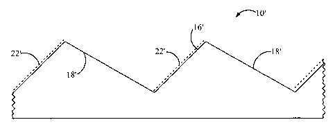
Fig. 1 is the schematic profile of the groove pattern of a prior art
diffraction
grating 10. Grating 10 consists of a substrate 12 having a plurality of
grooves 14
formed therein. The grooves are defined by adjacent transverse, planar steps
16 and
risers 18. The planar steps 16 are a reflective surface in that they reflect
an incident
light beam. The planar risers 18 are a non-reflective surface in that they do
not reflect
an incident light beam with the grating configured to receive an incident beam
as
illustrated by the sine wave 24 of Fig. 1. Adjacent steps and risers have an
apex 20
directed away from the substrate with a select angle (a) between the adjacent
steps and
risers 16, 18. As illustrated in Fig. 1, both the steps and the risers are
coated with a
conductive reflective coating, typically a metallic reflective coating 22 such
as gold.
A sine wave 24 is drawn in Fig. 1 to represent the oscillating electric field
of (s)
polarized light in the "TM" (transverse magnetic) direction of polarization.
The
incident light is reflected off the reflective surface or planar step 16. This
electric field
oscillates in a plane perpendicular to the grating grooves and perpendicular
to the plane
of riser 18. The orthogonal oscillating reflective field of (p) polarized
light or the "TE"
(transverse electric) direction of polarization oscillates parallel to the
grating grooves.
It is known that the diffraction efficiency for the TE and TM components of
the
diffracted light are different in diffraction gratings. While there is no
intention to limit
the scope of this disclosure or the appended claims by this statement of
theory, one at
CA 02406458 2002-10-04
WO 01/77738 PCT/USO1/11146
7
least partial explanation for the different diffraction efficiency of the
orthogonal
components of polarized light is that the conductive coating on the riser
surface
interferes with the electric field. This phenomenon is illustrated graphically
in Fig. 2.
Fig. 2 is a representation of field strength on the Y axis versus distance
from the riser
on the X axis. The field strength ES at the riser is zero. In contrast, the
electric field
vector of the (p) polarized light, which is parallel to the grating rulings
and
perpendicular to the plane of the (s) polarized light, does not sample the
region near the
grating riser. Thus, there are minimal boundary conditions imposed by the
grating riser
and at the riser Ep ~ 0. It is the change in boundary conditions that is
believed to be one
factor increasing the polarization dependence of the grating.
Fig. 3 illustrates a modification to the grating 10 of Fig. 1 for minimizing
polarization dependent loss of the grating. The grating 10' has a reflective
coating 22'
on the reflective steps 16' only, and no reflective coating on the risers 18',
which form a
non-reflective surface that does not reflect an incident beam. This eliminates
the
boundary condition imposed by the conductive coating on the grating riser as
illustrated
in Fig. 2, and for that reason is believed to decrease polarization dependent
loss.
An alternative to eliminating the boundary condition imposed by the riser (or
non-reflective surface) by not applying a conductive coating to the riser is
to use a
mufti-layer dielectric coating in place of the conductive reflective coating
22 in the
prior art embodiment depicted of Fig. 1. The mufti-layer dielectric coating
could be
made of any one of a number of highly reflective mufti-layer dielectric
coatings known
in the art, including layered titanium dioxide (TiOz) and silicon dioxide
(Si02); layered
tantalum pentoxide (Ta305) and silicon dioxide (Si02); and layered halfnium
dioxide
(Hf02) and silicon dioxide (SiOz). The mufti-layer dielectric coatings have
the
advantage of being more highly reflective than simple metal coatings, possibly
exceeding 99.9% efficiency. Because these dielectric coatings are necessarily
nonconductive, they ensure that the TE and TM components of the electric field
sample
similar boundary conditions. Thus, application of the dielectric coating
offers the
potential of higher efficiency and decreased polarization dependent loss. The
dielectric
coating may also be applied only to the reflective surface as is the case with
the
conductive reflective coating 22' depicted in Fig. 3. Similarly, the
dielectric coating
CA 02406458 2002-10-04
WO 01/77738 PCT/USO1/11146
may be used in any other embodiment employing a reflective conducting coating
such
as those shown in Figs. 4 and 5 or holographic gratings (which are not
illustrated).
The gratings disclosed herein may be formed from one of several known
methods. For example, it may be formed from an epoxy layer deposited on a
glass
substrate into which a master die defining the grooves is pressed. The grooves
may also
be precision machined directly into a glass or silicon substrate by an
interferametrically
controlled ruling engine. A further option is the use of photolithographic
techniques
described in McMahon, U.S. Patent No. 4,736,360, the contents of which are
hereby
expressly incorporated by reference in its entirety.
Coating of only the steps (i.e., the reflective surface) can be accomplished
using
coating techniques that employ a highly directional beam of reflective coating
material
(e.g., ion beam sputtering) or by coating the entire grating surface with the
reflective
coating using known techniques and ion etching the coating from the risers (or
non-
reflective surface). The reflective coating may be any suitably reflective
material, and
is typically a metallic conductive reflective coating such as gold, although
as discussed
above dielectric coatings may be preferred.
While not intending to be limiting on the scope of the disclosure, the
following
example illustrates that providing the reflective coating on the reflective
steps of a
grating and not on the riser can be effective in reducing polarization
dependent loss.
Fig. 4 is a schematic profile of groove pattern of a diffraction grating 28.
The
grating 28 consists of a plurality of grooves 30 formed in a substrate 32.
Each groove is
defined by a transverse step 34 and riser 36 that are joined in the groove
trough by a flat
38. In this example, the entire surface of the grooves, including the
reflective step 34,
the flat 38 and the riser 36 are covered by a conductive reflective coating 40
of gold.
The groove density is 171.4 grooves per millimeter , the blaze angle, 66, is
31 °, the
groove depth is about 2500.0 nm, the flat 38 is about 713.0 nm long, and the
apex
angle, aa, is 80°.
Fig. 5 is a profile of the groove pattern of a diffraction grating 28' which
is
identical to the diffraction grating 28 in all respects except the surface of
the risers 36'
does not have the conductive reflective coating 40'. Thus, the reflective step
and the
flat 38' are the only parts of the grating surface that are coated.
CA 02406458 2002-10-04
WO 01/77738 PCT/USO1/11146
9
Fig. 6 is a graph of efficiency versus wavelength for the TE and TM
components of a refracted optical signal as a function of wavelength. The
efficiency is
the ratio of the energy content of the diffracted light of the respective TE
and TM
component and the energy content of the light incident on the grating. For the
C band
of wavelengths which is currently used for optical communication (?~ = 1528 -
1565
nm) the polarization dependent loss, measured as the difference in efficiency
between
the TE and TM components, varies between about 10 - 16 percent.
Fig. 7 illustrates the polarization dependent loss for the grating 28'
illustrated in
Fig. 5 where only the reflective steps 34' are coated. Here the polarization
dependent
loss is sharply reduced, varying between about 2.5 - 5 percent.
Not providing a reflective coating on the riser of a grating in accordance
with
the present invention decreases polarization dependent loss inherent in bulk
diffraction
gratings. It does not require alteration of the grating profile which could
detrimentally
effect the ability of the grating to provide necessary channel separation,
resolution and
efficiency. Use of a dielectric reflective coating can yield similar
advantages.
Furthermore, these advantages can be provided to known grating profiles
including but
not limited to the embodiments illustrated herein and holographic gratings,
with
minimal effort and expense.