Note : Les descriptions sont présentées dans la langue officielle dans laquelle elles ont été soumises.
CA 02424027 2003-03-28
GCSD-1221 (H7150)
SPTRAL WOUND, SERIES FED, ARRAY ANTENNA
Field of the Invention
[0001] The present invention relates to phased array
antennae, and more particularly, this invention relates
to series fed phased array antennae.
Background of the Invention
[0002] Low cost phased array antennae are required on
naval ships, land based radar stations and similar areas.
Some traditional phased array antennae use periodic or
spiral lattices and transmit/receive modules that are
prohibitive in cost. When an antenna is designed for use
with short wavelengths in advanced radar designs, a low
side lobe architecture is required.
[0003] One type of phased array antenna architecture
uses a Dual Application Program (DUAP) array structure
based on a typical dual beam and corporate radio
frequency and digital feed network. It typically
includes a multilayer circuit board having various layers
for different circuit components, including low noise
amplifiers, phase shifters and other assorted feed lines,
1
CA 02424027 2003-03-28
GCSD-1221 (H7150)
signal traces and component devices. For multiple beam
and multiple polarization arrays, however, this type of
antenna structure requires a complicated printed wiring
board having multiple interconnects. For example, some
printed wiring boards include over two thousand (2,000)
vias in an 18-inch square printed circuit card, 64
elements, and two antenna beams. Not only is the layout
of this array difficult to achieve, it can surpass some
existing radio frequency layout tool capacities. This
type of antenna architecture also requires a complicated
feed network and multilayer circuit board with
complicated circuit components that should not cross-
over, thus, increasing design and construction
difficulty.
[0004] Many phased array antennae use corporate feed
networks with complicated interconnect systems because a
corporate fed antenna allows a wide bandwidth. Also, in
a planar array having a corporate feed network, the
periodic spacing and phase settings between the antenna
elements require only a simple sine calculation. The
corporate feed network can typically provide an
advantageous impedance match. Unfortunately, a corporate
feed network is usually complicated and is often designed
into an antenna structure from habit and not from
advantage.
[0005] A linear, series fed array, however, will not
have the complicated design drawbacks associated with a
corporate feed network. Some linear, series fed arrays
have been built as early as the 1940's. For example, the
United States Navy built a phased array series of fed WG
slot arrays used to scan the beam. These type of linear,
2
CA 02424027 2003-03-28
GCSD-1221 (H7150)
series fed arrays, however, were limited in their use
because of frequency scan effects and the grating lobes.
Summary of the Invention
[0006] In view of the foregoing background, it is
therefore an object of the present invention to provide a
series fed array antenna that overcomes the drawbacks
associated with prior art linear series fed array
antennae.
[0007] It is also an object of the present invention
to provide a series fed antenna array that breaks up
frequency scan effects and grating lobes.
[0008] It is yet another object of the present
invention to provide a low cost antenna array that
simplifies layout and eliminates crossover drawbacks
associated complicated corporate feed networks.
[0009] These and other objects, features and
advantages in accordance with the present invention are
provided by a phased array antenna that includes a
circuit board and a balanced, series fed antenna array
formed from a plurality of antenna elements positioned in
at least two spiral antenna arms on the circuit board.
At least one signal feed point is positioned at a center
portion of the spiral antenna arms for series feeding the
antenna array, such that the antenna aids in breaking up
frequency scan and grating lobes. In one aspect of the
present invention, electronic circuitry can be supported
by the circuit board and operatively connected to the
antenna elements for amplifying, phase shifting and beam
forming any transmitted or received signals.
3
CA 02424027 2003-03-28
m GCSD-1221 (H7150)
[0010] In another aspect of the present invention, the
antenna array is formed as two balanced series fed
antenna arrays, each formed as spiral antenna arms and
having dual feed points. The circuit board could be
formed as a multilayer circuit board having a microstrip
layer operative with the antenna elements for series
driving the antenna array. The number of antenna
elements within each spiral antenna arm are substantially
the same and can be formed as either surface mounted
antenna elements or printed antenna elements.
[0011] In yet another aspect of the present invention,
the plurality of antenna elements are arranged on the
circuit board in four spiral antenna arms as balanced,
series fed antenna arrays having signal teed points at a
center portion of the spiral arm. The antenna elements
can be formed as respective 0, 90, 180 and 270 degree
spiral arms for phased operation.
[0012] In yet another aspect of the present invention,
the phased array antenna can comprise a balanced, series
fed antenna array formed from a plurality of antenna
elements positioned in at least two spiral antenna arms
on the circuit board and having at least one signal feed
point at a center portion of the spiral antenna arms for
series feeding the antenna array. The spiral arms can be
formed from a waveguide having slots defining the antenna
elements. If a waveguide is not used, then the antenna
elements can be positioned on a planar circuit board as
described before.
4
CA 02424027 2003-03-28
GCSD-1221 (H7150)
Brief Description of the Drawings
[0013] Other objects, features and advantages of the
present invention will become apparent from the detailed
description of the invention which follows, when
considered in light of the accompanying drawings in
which:
[0014] FIG. 1 is a fragmentary view of a linear,
series fed array antenna showing individual antenna
elements that can be controlled by appropriate phase
shift devices.
[0015] FIGS. 2-5 are fragmentary, plan views of the
respective spiral arms shown as a single spiral arm in
FIGS. 2 and 4 and dual spiral arms in FIGS. 4 and 5.
[0016] FIG. 6 is a fragmentary plan view of two
balanced, series fed arrays such as shown in FIGS. 3 and
that are wrapped in a spiral configuration with 0, 90,
180, and 270 degree spiral arms.
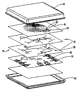
[0017] FIG. 7 is an exploded, isometric view of the
series fed phased array antenna of the present invention
as formed from a single, multilayer printed circuit board
and showing different layers for supporting various
amplifier elements, beam forming network, phase shifters
and packaging components.
[0018] FIG. 8 illustrates a waveguide that could be
configured in a spiral configuration in accordance with
the present invention.
Detailed Description of the Preferred Embodiments
[0019] The present invention will now be described
more fully hereinafter with reference to the accompanying
drawings, in which preferred embodiments of the invention
5
CA 02424027 2003-03-28
GCSD-1221 (H7150)
are shown. This invention may, however, be embodied in
many different forms and should not be construed as
limited to the embodiments set forth herein. Rather,
these embodiments are provided so that this disclosure
will be thorough and complete, and will fully convey the
scope of the invention to those skilled in the art. Like
numbers refer to like elements throughout, and prime
notation is used to indicate similar elements in
alternative embodiments.
[0020] The present invention advantageously provides a
phased array antenna that includes a balanced, series
fed, phased array antenna formed from a plurality of
antenna elements positioned in at least two spiral
antenna arms on a circuit board. At least one signal
feed point is provided at a center portion of the spiral
antenna arms for series feeding the antenna array and
conducting any transmitted or received signals to aid in
breaking up frequency scan and grating lobes.
[0021] This new class of~ series fed antenna array is
advantageous over prior art linear, series fed antenna
arrays that do not break up the frequency scan and
grating lobes as in the present invention. The present
invention also simplifies the physical construction of an
array antenna built on printed circuit boards and cuts
non-reoccurring engineering (NRE) costs while allowing a
simple layout for antenna elements, signal feed circuits,
and associated components. The spiral configuration of
the present invention can be applied to numerous multiple
beam lengths, including TCDL, CDL-N, and DD XX
structures. The design of the present invention can cut
costs and non-reoccurring engineering aspects on all
6
CA 02424027 2003-03-28
GCSD-1221 (H7150)
arrays with estimated cuts of 50% and schedule cuts of
six months. Production cuts can be lowered from about
10% to about 50%.
[0022) FIG. 1 illustrates at 10 a prior art linear,
series fed array antenna having numerous interconnected
antenna elements 12 using phase shift components 14
(shown by the arrow) and other driving elements and
signal circuits as known to those skilled in the art.
This type of linear, series fed array could be formed on
a multilayer circuit board by techniques as known to
those skilled in the art. A feed point 16 is positioned
at the center of the linear array 10 and includes two
signal feed line terminals 18,20 in which a signal
voltage is placed across the terminals as known to those
skilled in the art. The array is terminated at either
end by appropriate terminations 22 to ground.
[0023] In accordance with the present invention, a
phased array antenna is formed as series fed antenna
array 30 (FIG. 6) that is wound in a spiral as shown in
the various spiral arms of FIGS. 2-S. One spiral arm is
shown in FIG. 2 and depicts a closely spaced single
spiral arm, with FIG. 3 illustrating the two spiral arms
formed when the linear array as in FIG, 1 is wrapped
about itself in a spiral with feed points positioned in
the center portion and forming a balanced; series fed
array. FIG. 4 shows a loosely formed single spiral arm
for the spiral arms shown in FIG. 5 and forming a second,
balanced, series fed array. The spiral arms combine
together to form a spiral series fed array 30 as shown in
FIG. 6, and showing two balanced; series fed arrays
wrapped in the spiral configuration that breaks up
7
CA 02424027 2003-03-28
GCSD-1221 (H7150)
frequency scan and grating lobes. A pair of dual feed
points or four signal feed "starts" 32a, 32b, 34a,:34b
are shown for each dual spiral that could be formed from
two linear, series fed antennae wound in a spiral. The
illustrated spiral wound series fed antenna shown in FIG.
6 has the four signal feed points or starts 32a, 32b,
34a, 34b and four spiral arms 36a, 36b, 38a; 38b with
over one thousand X1,000) antenna elements. This
structure forms a quad drive having dual feed points for
the four starts as illustrated. This forms a simple
circuit structure to feed an antenna array. The
illustrated four spiral arms 36a, 36b, 38a, 38b having
the four spiral signal feed starts 32a, 32b, 34a, 34b
have antenna elements that are positioned on the circuit
board and spiral wound to form a respective 0 degree
spiral arms as 36b; a 90 degree spiral arm as 36a; a 180
degree spiral arm as 38a; and a 270 degree spiral arm as
38b. The illustrated antenna structure has a high
aperture efficiency using 0.63662 wavelength spacing with
7.7815 dBi antenna elements in one non-limiting example.
Numerical wavelength lamda values are shown on the
respective x,y axis with respect to the positioning of
the various antenna elements.
[0024] A non-limiting example of a lattice support
structure for the antenna of the present invention is
shown in FIG. 7, and could include a radome 40 and
radiating antenna elements formed in the spiral
configuration as a series fed array and positioned on one
multilayer circuit board 44. A top layer 46 of the board
includes the antenna elements 48, and in some designs,
even amplifier elements 50, including low noise
8
CA 02424027 2003-03-28
GCSD-1221 (H7150)
amplifiers (LNA) or other components. The antenna
elements 48 can be surface mounted or,printed by
techniques known to those skilled in the art. A bottom
layer portion 52 of the board can include, for instance,
phase shifters, post amplification circuit elements with
combiners and beam steering elements and other components
54. A middle layer portion 56 (such as two layers) can
include a beam former network with power combining and
signal distribution 58. Other layers can include beam
control components, filtering or other components, which
can exist combined on some layers or on separate layers.
One or more microstrip layers are operative for
conducting signals and driving the array. The layers can
be formed by techniques known to those skilled in the
art, including green tape layers. Mechanical packaging
components 60 can include basic power supplies, cooling
circuits and packaging. Such a structure can then be
placed in another support structure and form part of a
lattice as an integral element.
[0025] FIG. 8 illustrates a waveguide 70 such as known
to those skilled in the art that can be wound in a spiral
to form a spiral wound, series fed array. The waveguide
70 includes a feed 72 and a plurality of slots 74 as
known to those skilled in the art. The slots 74 could be
less vertical as they extend from the center portion of
the waveguide. Coupling could be a function of the angle
of the. slot.
[0026] It is evident that the present invention now
provides a series fed array antenna wrapped in a spiral
configuration that is advantageous over prior art linear,
9
CA 02424027 2003-03-28
GCSD-1221 (H7150)
series fed arrays to break up frequency scan and grating
lobes.
[0027 Many modifications and other embodiments of the
invention will come to the mind of one skilled in the art
having the benefit of the teachings presented in the
foregoing descriptions and the associated drawings.
Therefore, it is understood that the invention is not to
be limited to the specific embodiments disclosed, and
that modifications and embodiments are intended to be
included within the scope of the appended claims.
10