Note : Les descriptions sont présentées dans la langue officielle dans laquelle elles ont été soumises.
CA 02427039 2003-04-29
- 1 -
HIGH SPEED BI-DIRECTIONAL SOLID STATE SWITCH
FIELD OF THE INVENTION
This invention relates to hi-directional solid state switches, and more
particularly to high-speed hi-directional solid state switches.
BACKGROUND OF THE INVENTION
In the prior art there are basically two types of bi-directional solid state
switches which are commonly used. One is the triac, which is commonly used for
switching AC (alternating current) power, and the other is the analog switch
based on
field effect transistors.
to Triacs suffer from two major problems. The first is that once triggered,
they
remain in the on-state until the next zero crossing in the AC voltage. The
other
problem is that the device inherently has a voltage drop associated with it,
which
results in significant power dissipation.
Switches based on field effect transistors have been very successfully used
for
switching low-level analog signals, however, various technical difficulties
have
prevented their widespread acceptance for AC power switching applications.
Referring now to Figure 1, it is demonstrated how a single NPN bipolar
transistor together with a diode bridge can form a simple AC switch. The NPN
bipolar transistor is only capable of switching on in one direction, however,
the diode
bridge changes the AC at the switch terminals into DC (direct current) going
through
the transistor.
It can be appreciated that such a switch can only work if the control signal
to
the transistor is in some way isolated from the AC power voltage. One method
of
doing this, which is well known in the prior art, illustrated in Figure 2, is
to use an
isolation transformer. Isolation transformers do not work on DC voltages,
however, if
an AC voltage is provided to the transformer input, a diode bridge on the
output of the
transformer can convert it into a DC voltage signal suitable for driving the
input of the
bipolar transistor. Still, such a switch is far from ideal due to power
dissipation in the
diodes and the bipolar transistor. This is due to the inherent voltage drops
in these
CA 02427039 2003-04-29
- _
devices. A bipolar transistor which is fully on, will have a voltage drop of
at least 0.3
Volts, however this voltage drop can be as high as 1 V or even higher
depending on
the transistor. Diodes have an inherent voltage drop of approximately 0.7 V,
and
since the AC would have to flow through two diodes plus the transistor, a
total
voltage drop across the switch would be on the order of 2 Volts. This means
that the
power dissipation will be about 2 Watts for every Amp flowing through the
switch.
Referring now to Figure 3 it is shown how power dissipation can be greatly
reduced through the use of field effect transistors, however, the problem of
isolation
between the AC voltage and the control signal remains. Since field effect
transistors
It) can conduct in both directions when they are in the on-state. there is
no need for a
diode bridge. However, field effect transistors will only block voltage in one
direction when in the off-state. Therefore, if they are used in an AC switch
(without a
diode bridge), there must be two of them connected in series in opposite
directions,
either having a common source as shown in Figure 3, or having a common drain
as
shown in Figure 5. The prior art method of isolation presented in Figure 3
suffers
from a number of problems. One is the size, weight, and cost of the isolation
transformer. Another is the complexity of the control circuit which must
generate AC
control signals to drive the isolation transformer. Finally, there is a loss
of speed of
response due to the frequency limitation of the transformer and the
rectification
circuit.
Referring now to Figure 4, another approach to isolation is shown which is
most commonly used in the prior art. In this instance the control signal
drives a series
of light emitting diodes in a photo-voltaic isolator. Photo-voltaic cells in
the isolator
receive the light energy from the light emitting diodes and convert it to
control signals
suitable for driving the field effect transistors. This approach eliminates
the bulky
expensive isolation transformer, and simplifies the circuit. The two major
drawbacks
of this approach are the cost of the photo-voltaic isolator, and its slow
speed of
response. Solid state relays based on this technology typically have response
times in
the millisecond range.
The idea of connecting two field effect transistors (FET) together in a common
source configuration is known. Huth et al show just such a configuration in
U.S.
CA 02427039 2012-05-29
- 3
Patent No. 3i532;8.99 issued October 6, 1970, for the purpose of providing a
solid state
switch for switching analog signals. However, Huth et al do not give any
details on how
to drive the field :effect transistor inputs while maintaining adequate
separation between
the control signal for the switch and the analog signals being switched,
5 McDonald in U.S. Patent 4,611,123 issued September 9, 1986, also
proposes a
=
solid state sWiteh: consisting of two field effect transistors in a common
source
an-angernent, and proposes a method of driving the field effect transistor
inputs.
However, his field effect transistor signal input driver involves the use of
optical
= isolation, Optical isOlation is a valid technical ablution, however it
does have certain
,
10 drawbacks. n particular, it makes the circuit more complicated, it adds
to the cost, and it
. slows down. the Speed of the device.
= Sorchych in US, Patent No. 3,215,859 issued November 2, 1965, proposes a
method of Controlling field effect transistors without the use of signal
isolation. Power
supply isolation is also not required by the method which he proposes.
However, his
15 circuit is only sUitable for switching low level analog signals. Any AC
voltage of 120 V
= would subject his bipolar transistors, used as drivers, to excessive
emitter-base voltages
which would damage the devices. This makes Sorchych's device unsuitable for
use as a
power switch in imany typical applications.
.1aesclake in U.S. Patent No. 4,480,201 issued October 30, 1984, provides a
more
20 robust method of driving the main switch transistors, however he uses
bipolar transistors
instead of field effect transistors for the output stage, choosing rather to
use field effect
transistors to linprOVe. the performance of :the bipolar transistors. The
result is a circuit
which is not partietilarly energy-efficient. Any AC power going through the
switch must
pass through one diode having a diode drop of 0.7 Volts and one power
transistor having
25 a voltage drop of at least 0.3 Volts resulting in an overall voltage
drop of at least 1 V.
This results a ',ewer dissipation of at least: One Watt per Amp.
Laughton in U.S. Patent No. 4,591,734 issued May 27, 1986, demonstrates the
use of insulated gate bipolar transistors (ICBT) for the output of his AC
switch. In
=
CA 02427039 2012-05-29
=
=
-4.
addition to the prohlerri of high power dissipation resulting from the voltage
drop across
the instilated gate bipolar transistors and diodes in the circuit, this
circuit has limited use
because 1,aughton grounds the emitters of the insulated gate bipolar
transistors. This
eliminates the heed to isolate the signal input, however, this circuit can
only be used
= 5 where the AC voltage is isolated. In most cases this
would require an expensive power
isolation ttanSfOrrner, which would of course be more costly than a signal
isolation
transformer.
Chang et al in U.S. Patent No. 4,142,380 issued May 3, 1988, show an AC switch
which makes : use of bipolar transistors, field effect transistors and
thyristors. For this
=
,== =... to circuit to work properly, the emitter of the PNP
transistor would need to he higher than
the AC voltage, The result of this is the need for =a high voltage DC power
supply.
Furthermore, this would not be a particularly energy efficient switch due to
resistors in
series With the field effect transistors, and: the voltage drops across the
thyristors. In
addition to these drawbacks the control would be limited, because once
triggered, the
=
15 thyristors would remain on until the next zero crossing in the AC
voltage,
=
.Janutka in U.S. Patent No, 4,477,742 issued October 16, 1984, shows an AC
=
switch with a common drain configuration. In this circuit the gates of the two
field effect
transistors are tiCci together. The result of this:is, that the voltage
capability of the switch
is limited by the gate7source breakdown voltages of the field effect
transistors which is
= .! , 20 typically 20 'Volts,: This makes the circuit
unsuitable for typical power applications
which require substantially higher voltages.
Siacki in U.S..: Patent No. 5,003,246 issued March 26, 1991, also provides a
common drain configuration. There are at least four problems with this
circuit. Firstly, it
has field effect transistors with common gates and output terminals connected
across the
25 full AC voltage. The result of this is that the voltage capability of
the switch is limited by
the gate-source Voltage Capability of these field effect transistors. Another
problem is
=
that the switch does not
=
=
:=
CA 02427039 2003-04-29
- 5 -
respond immediately to activating control signals, but rather waits for the
next zero
crossing before turning on. The third problem has to do with energy
efficiency. To
be energy-efficient, the control resistor R1 must have a high resistance value
because
it is loaded with almost the entire AC voltage. However, a consequence of this
resistor having a high value is that the speed of response of the switch is
slowed down
considerably due to the gate capacitance of the field effect transistor TP2.
One could,
of course, speed up the switch by lowering the resistance of the resistor R1,
but that
would result in increased power dissipation in the resistor due to the high-
voltage AC.
Finally, it should be noted that the switch never really turns fully off
because of
current flowing through the control resistor RI when the switch is in the off-
state.
BRIEF SUMMARY OF THE INVENTION
'[he invention overcomes these disadvantages by providing a high speed bi-
directional solid state switch wherein the control input and load output share
a
common terminal, which may be grounded, and which operates without any
IS requirement for isolation. The switch can be turned on or off at any
time, at or
between zero crossings. The bi-directional solid state power switch of the
invention is
simple, reliable, cost-effective, energy-efficient, and possesses a high speed
of
response.
According to a preferred embodiment of the invention, two field effect
transistors are connected with gate connected to gate and source connected to
source.
Each drain is separately connected to a switch output terminal. A resistor is
connected between the gate connection and the source connection. The driver
signal
is connected across the gate connection and one of the drain terminals. This
circuit
topology provides aforementioned advantages, and does not need electrical
isolation.
The present invention thus provides a bi-directional solid state switch
comprising at least two main transistors, each comprising a control terminal,
a second
terminal referenced to the control terminal, and a third terminal for
conducting an
electric current between the second and third terminals; the control terminals
of the
two main transistors being electrically connected and the second terminals of
the two
main transistors being electrically connected, the control terminals being
electrically
connected to the second terminals through at least one device having an
impedance, a
CA 02427039 2003-04-29
- 6 -
first switch control input for connection to the control terminals of the two
main
transistors, for selectively applying an activating control signal from one
side of an
electric signal source, and a second switch control input tbr connecting the
third
terminal of one of the main transistors to the other side of the electric
signal source,
wherein when the activating control signal is applied to the switch control
inputs, an
electric current can be conducted through the main transistors.
BRIEF DESCRIPTION OF THE DRAWINGS
FIG. 1. is a schematic circuit diagram showing an AC solid state switch which
comprises a diode bridge and a bipolar transistor.
FIG. 2. is a schematic circuit diagram showing an AC solid state switch which
comprises a diode bridge and a bipolar transistor, wherein an isolating
transformer is
used to provide the required isolation between input and output.
FIG. 3. is a schematic circuit diagram showing an AC solid state switch
comprising
field effect transistors, where an isolating transformer is used to provide
the required
isolation between input and output.
FIG. 4. is a schematic circuit diagram showing an AC solid state switch
comprising
two field effect transistors. wherein a photo-voltaic isolator is used to
drive the
transistors and provide the required isolation between input and output.
FIG. 5. is a schematic circuit diagram showing an AC solid state switch
comprising
two field effect transistors wherein the transistors have their drains
connected
together.
FIG. 6. is a schematic circuit diagram showing an AC solid state switch in
accordance
with the present invention.
FIG. 7. is a schematic diagram showing an AC solid state switch in accordance
with a
preferred embodiment of the present invention, wherein the driver circuit
comprises
bipolar transistors.
CA 02427039 2003-04-29
- 7 -
FIG. 8. is a schematic diagram showing an AC solid state switch in accordance
with
an alternative preferred embodiment of the present invention, wherein the
driver
circuit comprises field effect transistors.
FIG. 9. is a graph showing electrical waveforms of the present invention.
DETAILED DESCRIPTION OF THE INVENTION
Referring now to the prior art bi-directional switching device shown in Figure
5, in this solid state switching circuit where one output terminal of the
switch is
connected to ground or connected in common with the ground reference of the
control
signal, it is intuitive that the source of a field effect transistor (FET) be
connected to
ground or common. This is because it is the voltage between the gate and the
source
that determines whether the field effect transistor is on or off. In other
words, the
source is the terminal which is referenced to the control terminal (or gate),
while the
drain is the unreferenced terminal and allows current to flow between it and
the
referenced terminal in both directions when the device is in the on-state. If
the circuit
is required to be bi-directional or required to switch AC, then a second field
effect
transistor is required to be connected in series and in the opposing direction
as shown.
This is because a field effect transistor can block voltage in one direction
only.
Consequently, the intuitive approach leads to a common drain circuit topology
for a
field effect transistor switching circuit if that circuit is required to
switch AC and if
one of the switch output terminals is connected in common with the reference
terminal of the control signal.
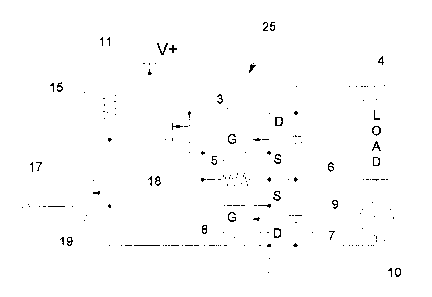
A preferred embodiment of the invention is illustrated in Figure 6, in which
the drain D of field effect transistor 8 is connected to the ground terminal.
Switch 2,
which is controllable. acts in combination with battery I as an electric
signal source.
One side of battery 1, which acts as a source of electricity, is connected to
a terminal
of switch 2, the other terminal of which in turn is connected to both gates G
and,
through resistor 5, to both sources S. The drain of field effect transistor 3
is
connected to one side of the load 4, the other side of the load 4 being
connected to one
terminal of the AC power supply 10. The other terminal of the AC power supply
10
is connected to drain D of field effect transistor 8, which is also connected
to the other
side of battery 1. In this instance, the connection point of the gates G acts
as a first
CA 02427039 2003-04-29
- 8 -
switch control input, while the drain D of field effect transistor 8 acts as a
second
switch control input (in the embodiment shown, both drain D of field effect
transistor
8 and the negative side of battery 1 are grounded, but as will be explained
below this
is unnecessary as long as they are electrically connected). Connecting the
drain D of
field effect transistor 8 to the ground or common terminal is
counterintuitive,
however, this approach provides significant advantages.
In operation, if switch 2 is open, then resistor 5 causes the gate-to-source
voltage of the two main field effect transistors 3 and 8 to be zero, causing
both
transistors 3 and 8 to be turned off In this state the two transistors will
block the AC
voltage coming from AC voltage source 10, and through AC load 4, in both
directions. Although zener diodes 6 and 7 are shown as circuit elements, it
will be
understood that typically each of these diodes 6, 7 is inherent to or
integrated into its
respective field effect transistor 3 and 8, but zener diodes 6 and 7 could
alternatively
be separate circuit components. It will be appreciated that resistor 5 could
be replaced
by a different component having an impedance, such as an inductor, or a
semiconductor device which may or may not itself be controllable, or even by a
combination of devices which have an impedance. Such alternatives may enhance
performance under certain conditions such as high frequency operation, and may
contribute to increased efficiency. Such a device which has an impedance could
also
be made to be inherent to or integrated into at least one transistor. It will
also be
appreciated that although field effect transistors 3 and 8 are preferably
identical, they
do not need to be identical for the advantages of the invention to be
achieved, and that
the other side of battery I could be connected to the drain D of either field
effect
transistor 3 or 8.
If switch 2 is closed, then the voltage from battery 1 is applied between the
gate G and drain D of field effect transistor 8 (to the gate G through switch
2 and to
the drain D through the ground terminal). Depending on the instantaneous
polarity of
the AC power, either diode 6 or diode 7 will then enable current to flow
through
resistor 5. The result of this is that a voltage will appear across the gates
G and
sources S of both transistors 3 and 8. Both transistors 3 and 8 will then be
turned on
and conduct in both directions. Because of diode 7, the common source
connection 9
CA 02427039 2003-04-29
- 9 -
will not have a voltage higher than approximately 0.7 Volts (which is less
than the
voltage from battery 1), and therefore switch 2 only needs to block voltage in
one
direction. As a result, switch 2 can be replaced by any transistor, including
a field
effect transistor, a bipolar transistor, an IGBT (insulated gate bipolar
transistor), or
any functional equivalent.
Referring now to Figure 7, in this embodiment of the invention the control
signal is provided to the field effect transistors 3, 8 by a driver circuit
comprising
bipolar PNP transistor 12. Bipolar PNP transistor 12 is turned on by bipolar
NPN
transistor 13, whenever a sufficiently positive activating control signal is
applied to
input terminal 17. Resistor 16 serves to limit the base current of bipolar NPN
transistor 13. while resistor 14 serves to limit the base current of bipolar
PNP
transistor 12. Resistor 15 maintains PNP transistor 12 in an off-state in the
absence of
an activating control signal at terminal 17, by removing any leakage current
which
may exist. The DC voltage source 11 provides the low gate voltage required by
the
IS field effect transistors 3 and 8. lithe field effect transistors 3 and 8
are logic level
field effect transistors, then this voltage can be as low as 5 or 6 Volts.
Figure 8 illustrates an alternate preferred embodiment of the present
invention,
in which the driver circuit comprises field effect transistors 18 and 19
performing the
function of bipolar transistors 12 and 13 of Figure 7. In this instance,
resistor 15
provides the additional function of returning the switch to the off-state
after the
activating control signal is removed. If the circuit is constructed using
discrete
components, it may be more cost-effective to use bipolar transistors for the
driver
circuit as in Figure 7. If, however, the circuit is constructed as a
monolithic device, it
may be better for the driver to use field effect transistors as in Figure 8.
It should be noted that while the circuits of Figures 7 and 8 are both shown
to
be grounded, grounding is in fact unnecessary provided that both the control
signal
applied to input terminal 17 and the FET driver voltage source 11 are
referenced to
the same drain terminal D. However, AC power circuits typically are grounded,
which is one of the advantages of the present invention, because grounding the
AC
supply circuit does not pose a problem for the present invention, while it
does pose a
problem for some of the aforementioned prior art. While the ability to operate
CA 02427039 2003-04-29
- 10 -
without the need for isolation may be advantageous in certain applications,
the present
invention has other advantages, as referred to previously, which may make it
advantageous to use the present invention in applications where isolation is
required
anyway for other reasons.
As shown in Figure 9, waveform 20, which is shown by a dashed line,
represents the voltage which appears on the drain terminal D of the field
effect
transistor 3 in Figure 8 and is sinusoidal when switch 25 is turned off. The
voltage
21, 22 at the common source connection 9 in Figure 8 is shown by a solid line
in the
upper graph of Figure 9. During the positive portion of the AC waveform 20,
the
voltage 21 at the common source connection 9 is slightly above ground
potential due
to diode 7. For this reason, FET driver voltage source 11 only needs to be
slightly
higher than the on-state gate-to-source voltage requirement for field effect
transistors
3 and 8. During the negative portion of the AC waveform 20, the voltage 22 at
the
common source connection 9 is only slightly above the AC waveform voltage. As
a
is consequence, driver circuit transistor 18 must have a high voltage
capability (as must
driver circuit transistor 12 in Figure 7) if the switch 25 is used to switch
high voltage
AC. When the switch control signal 24 applied to terminal 17, shown by a solid
line
in the lower graph of Figure 9, exceeds the gate threshold voltage for driver
circuit
transistor 19, both voltages 20 and 21. 22 become almost zero. In this state,
the
switch 25 is turned fully on and the AC load 4 has full power. The switch 25
can be
turned on or off at any time and without any need to wait for zero crossings
in the AC
waveform 20.
Because there is no isolation to slow the switch 25 down, it has a very high
speed of response, in fact it may be orders of magnitude faster than a typical
optically-
isolated solid state relay. The circuit of the invention is very simple and
reliable and
very cost-effective, with most of the cost being in the field effect
transistors. It also
has the potential for being much more energy efficient than bipolar
transistors, triacs
and thyristors. Applications for this technology include but are not limited
to light
dimmers, motor controls, switch-mode power supplies, interface output modules,
signal generation, and remote and automatic controls.
CA 02427039 2003-04-29
- ii -
Preferred embodiments of the invention having been thus described by way of
example only, it will be appreciated that various modifications and
adaptations may
be made without departing from the scope of the invention as set out in the
appended
claims.