Note : Les descriptions sont présentées dans la langue officielle dans laquelle elles ont été soumises.
CA 02449131 2003-12-O1
WO 02/097462 PCT/AU02/00696
"Method and apparatus for magnetic field measurement"
Technical Field
The present invention relates to magnetic field measurement and in
particular provides a superconducting method and apparatus for magnetic field
measurement.
Background Art
Superconducting Quantum Interference Devices (SQUIDS) are often
used as highly sensitive magnetic field sensors. Such SQUID sensors are
Zo becoming increasingly popular due to the capabilities of high sensitivity
sensing
in areas such as geophysical mineral prospecting and biological magnetic field
detection, such as magnetic field emanations from the human brain.
With the advent of high critical temperature superconducting (HTS)
materials such as YBa2Cu30,~ (YBCO), HTS-SQUIDs can be cooled by
is relatively inexpensive liquid nitrogen, and can be made in a compact form.
The HTS radio frequency (rf) SQUID is essentially a superconducting
ring made of YBCO or the like, the ring being interrupted by a Josephson
Junction or weak link. When the superconducting ring is energised by an
inductively coupled resonant rt-oscillator, tunnelling of electrons takes
place at
2o the junction and a periodic signal, being a function of flux through the
ring, can
be detected across the junction. The periodic signal is substantially a
triangular
waveform, usually having a period (0B) in the order of a nanotesla. Therefore,
in order to yield a sensitivity in the femtotesla range, the SQUID is operated
in
a nulling bridge mode, or flux locked loop (FLL) mode. In this mode, magnetic
5 flux is fed back to the SQUID so as to cause the output voltage to remain
relatively constant. The feedback voltage, being proportional to the
difference
between the applied flux and the quiescent flux level, gives a highly accurate
measurement of relative magnetic flux. The feedback voltage V can therefore
be written as
30 V = M (Aef~B + u) (1 )
where
M is a constant in a specific SQUID system;
Aeff is the effective area of the SQUID;
B is the applied magnetic field; and
3s a is the quiescent flux.
CA 02449131 2003-12-O1
WO 02/097462 PCT/AU02/00696
2
However, since the quiescent flux a is unknown, SQUIDs provide only
relative measurements of magnetic field, and do not provide a measurement of
an absolute magnitude of magnetic field. Further, when the applied flux
changes too quickly, at a rate which is greater than the "slew rate" of the
SQUiD, the loop loses lock, and a discontinuous output results. Due to the
periodic nature of the SQUID response, it is not possible to determine from
the
output whether the SQUID has regained lock at a same position in the periodic
waveform, and thus such interrupted results are of limited use.
Any discussion of documents, acts, materials, devices, articles or the like
Zo which has been included in the present specification is solely for the
purpose of
providing a context for the present invention. It is not to be taken as an
admission that any or all of these matters form part of the prior art base or
were
common general knowledge in the field relevant to the present invention as it
existed before the priority date of each claim of this application.
Throughout this specification the word "comprise", or variations such as
"comprises" or "comprising", will be understood to imply the inclusion of a
stated element, integer or step, or group of elements, integers or steps, but
not
the exclusion of any other element, integer or step, or group of elements,
integers or steps.
o Throughout this specification, the terms 'superconducting material',
'superconducting device' and the like are used to refer to a material or
device
Which, in a certain state and at a certain temperature, is capable of
exhibiting
superconductivity. The use of such terms does not imply that the material or
device exhibits superconductivity in all states or at all temperatures.
Summary of the Invention
According to a first aspect the present invention resides in a method of
measurement of absolute magnitude of a magnetic field, the method
comprising the steps of:
3o providing a superconducting quantum interference device having an
effective flux-collection area which varies with applied flux; and
determining an absolute magnitude of an applied magnetic field based
on variations in said effective area.
According to a second aspect, the present invention provides a
superconducting quantum interterence device for measurement of absolute
CA 02449131 2003-12-O1
WO 02/097462 PCT/AU02/00696
3
magnitude of a magnetic field, the device having an efFective flux-collection
area which varies with applied flux.
It has been realised that periodicity of the output voltage function of a
SQUID relies on the effective area of the SQUID. Accordingly, providing a
SQUID with an effective area which alters or varies at one or more known
absolute values of flux density, enables the SQUID to detect when the one or
more known flux densities are applied, due to the changing periodicity of the
output voltage of the SQUID at those flux densities. Hence, absolute magnetic
field values may be measured by the SQUID.
1o Further, the absolute value of an applied flux which is different to the
one
or more known absolute values of flux may be determined with reference to the
one or more known flux densities. Accordingly, the method and device of the
present invention allow measurement of the absolute value of an applied field
to be measured, at least when the strength of that field is in the vicinity of
the
i5 one or more known flux values to allow comparison to the one or more known
flux values.
It has further been realised that provision of a flux-dam in the pick-up
loop of a SQUID is an effective manner in which to provide a SQUID having an
effective area which varies with applied flux. In such embodiments, the flux-
2o dam 'opens' and 'closes', depending on whether the circulating current in
the
pick-up loop is greater than or less than the critical current of the flux-
dam.
That is, the flux-dam becomes resistive when the circulating current in the
pick-
up loop exceeds the critical current of the flux-dam. As the circulating
current is
caused by applied flux, there exists a critical (and calculable) value of
applied
25 magnetic field at which the flux-dam becomes resistive. At that point, the
flux
dam becomes resistive, causing the effective area of the SQUID to change,
and so the periodicity of the output voltage of the SQUID changes, enabling
the
absolute value of the applied magnetic field to be measured. The absolute
value of an applied magnetic field of different magnitude to the critical
magnetic
ao field may be determined by reference to the critical magnetic field.
Accordingly, in a third aspect the present invention resides in a method
of measurement of absolute value of a magnetic field, the method comprising
the steps of:
providing a pick-up loop for a SQUID, the pick-up loop having a flux dam
35 having a critical current, the critical current occurring in the pick-up
loop when a
critical magnetic field is applied to the SQUID; and
CA 02449131 2003-12-O1
WO 02/097462 PCT/AU02/00696
4
determining an absolute value of an applied magnetic field by
comparison to said critical magnetic field.
The method of the third aspect of the present invention may further
comprise the step of fabricating the flux-dam such that the critical magnetic
s field is in a magnetic field range of interest.
According to a fourth aspect, the present invention resides in a pick-up
loop for a SQUID for measurement of absolute value of a magnetic field, the
pick-up loop having a flux dam having a critical current, the critical current
arising when a critical magnetic field is applied to the SQUID, and the flux
dam
Zo being formed such that the critical magnetic field is in a magnetic field
range of
interest.
The SQUID may comprise a superconducting ring of HTS material, such
as YBCO, interrupted by a Josephson Junction. The Josephson Junction may
be implemented by formation of a grain boundary in the HTS material, for
i5 example by forming the junction over a step-edge in a substrate. The step
edge could, for example, be formed in accordance with the teachings of
International Patent Publication No. WO 00/16414, the contents of which are
incorporated herein by reference. Of course, the Josephson Junction may be
formed in a different manner, for example by use of a microbridge, an ion-
2o irradiated link, a superconductor-insulator-superconductor (SIS) junction,
a
superconductor-normal metal-superconductor (SNS) junction or the like.
Similarly, where a flux-dam is used to provide an efFective area
dependent on flux, the flux dam may be implemented by forming a grain
boundary at a step edge in a substrate, or by use of a microbridge, or the
like.
25 Further, it will be appreciated that the present invention is applicable to
both rf-SQUIDs and dc-SQUIDs.
Brief Description of the Drawings
By way of example only, preferred embodiments of the invention are
3o described with reference to the accompanying drawings, in which:
Figure 1 illustrates a schematic block diagram of a flux-locked loop
suitable for operating a high-T~ rf SQUID;
Figure 2a is a graph which illustrates the variation of the amplitude of the
rf voltage across the tuned circuit as a function of the magnetic flux in the
35 SQUID chip;
CA 02449131 2003-12-O1
WO 02/097462 PCT/AU02/00696
Figures 2b and 2c illustrate quiescent magnetic field conditions and
departures therefrom;
Figures 3a and 3b depict the rf oscillation and envelope;
Figure 4 illustrates a dc-SQUID flux-locked loop;
5 Figure 5 is a schematic drawing of an rf SQUID with a pick-up loop
having a flux dam;
Figure 6 is a plot of pickup loop enclosed flux against the applied flux;
and
Figure 7 is a plot of the open loop SQUID output voltage and the applied
Zo magnetic field against time, illustrating the change in output voltage
periodicity
with changing field.
Description of the Invention
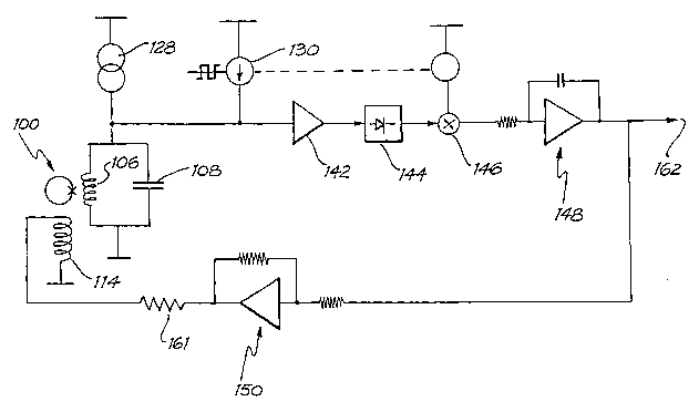
Figure 1 illustrates a schematic block diagram of a flux-locked loop
i5 suitable for operating a high-T~ rf SQUID 100. Radio frequency current
source
128 provides a sinusoidal current to drive the tuned circuit comprising rf
coil
106 in parallel with capacitor 108. Typically, the rf current has a frequency
ranging from 1 MHz to microwave frequencies, but preferably the frequency is
in
the range of 150MHz to 200MHz. The field from rf coil 106 is coupled to high-
2o T~ SQUID chip 100, and the amplitude of the rf voltage generated across the
tuned circuit is affected by the magnetic flux in the SQUID 100.
Figure 2a is a graph which illustrates the variation of the amplitude of the
rf voltage across the tuned circuit 106, 108 as a function of the magnetic
flux in
the SQUID chip 100. The amplitude is substantially a periodic, triangular-wave
25 function of the magnetic flux.
Current source 130 superimposes a square-wave onto the sinusoidal
current from source 128. Typically, the superimposed square-wave current has
a longer period than the sinusoidal current. Preferably, the period of the
square-wave current is of the order of ten microseconds. The effect of the
3o square-wave current is to alter the magnetic flux density in the SQUID chip
100. As shown in Figure 2b, the magnetic flux density to be measured sets up
a quiescent magnetic flux density 132 in the SQUID chip, and this results in
quiescent amplitude 134 of the rf voltage.
If the quiescent flux density is such that the amplitude of the rf voltage is
35 not at a maximum or minimum, as illustrated in Figure 2b, the superimposed
square wave flux oscillations 136 cause the amplitude of the rf voltage to
CA 02449131 2003-12-O1
WO 02/097462 PCT/AU02/00696
6
oscillate between levels 138 and.140. A typical waveform of the resulting rf
voltage is shown in Figure 3a. Alternatively, when the quiescent flux density
in
the SQUID chip is such that the amplitude of the rt voltage is at a maximum or
a minimum, as illustrated by flux density 143 in Figure 2c, the amplitude of
the
resulting rf voltage is constant at level 145.
The rf voltage across the tuned circuit is amplified by amplifier 142, and
its amplitude is detected by diode detector 144. The output of the diode
detector consists substantially of the square-wave envelope of the signal at
the
input of amplifier 142, as shown in Figure 8b. If the flux density is not at a
Zo minimum of the triangular waveform but, for example, is at level 132 as
shown
in Figure 2b, the amplitude of the detected waveform is proportional to the
difference between levels 140 and 138. Alternatively, if the quiescent flux
level
coincides with a maximum or a minimum in the triangular amplitude versus flux
density characteristic, as illustrated by flux density 142 of Figure 2c, the
z5 amplitude of the detected waveform will be approximately zero.
If the quiescent flux density is in a region in which the characteristic has
a positive slope, level 140 will be higher than level 138. In contrast, if the
quiescent flux density is in a region in which the characteristic has a
negative
slope, level 140 will be lower than level 138. Thus, the phase of the detected
2o waveform relative to the square-wave current depends on the slope of the
voltage versus flux characteristic at the quiescent level.
Multiplier 146 multiplies the detected voltage by a voltage which is in
phase with the square-wave current of source 130 to produce a product voltage
which varies according to the quiescent flux level and the phase of the
detected
5 voltage. The product voltage is zero if the quiescent flux level coincides
with a
minimum or a maximum of the amplitude versus flux characteristic, is at a
maximum positive level if the quiescent flux level is in the centre of a
positively
sloped section of the amplitude versus flux characteristic, and is at a
maximum
negative level if the quiescent flux level is in the centre of a negatively-
sloped
ao section of the amplitude versus flux characteristic.
The product voltage is integrated by integrator 148, amplified by variable
gain amplifier 150, and the resulting signal is used to energise feedback coil
114 via resistor 161 to subject SQUID chip 100 to a feedback magnetic flux
density.
35 The effect of the negative feedback is to apply a second magnetic flux
density to the SQUID chip such that the total magnetic flux density is
CA 02449131 2003-12-O1
WO 02/097462 PCT/AU02/00696
7
substantially constant. The output voltage of integrator 148 is, therefore,
indicative of the difFerence between the magnetic flux density to be measured
and the substantially constant magnetic flux density. Therefore, it can be
seen
that the device shown in Figure 1 does not measure absolute value of magnetic
field, but only a difference in magnetic flux density.
As shown in Figure 2c, which illustrates the amplitude versus flux
relationship in the flux-locked loop in equilibrium, the effect of the
feedback is to
drive the flux threading the SQUID to a constant value. The maximum rf
amplitude corresponds to an unstable equilibrium point in the flux-locked
loop,
Zo and deviation from this point will result in the loop converging to a
minimum rf
voltage.
Referring to Figure 4, a do SQUID flux-locked loop (FLL) is illustrated.
There are many variations and refinements possible but this is a typical basic
circuit. Much of it is similar to the rf SQUID flux-locked loop described with
i5 reference to Figure 1 and the operation can be explained with reference to
Figures 2 and 3b (but excluding 3a).
The current source 228 provides do current bias for the SQUID 200.
When correctly biased, the SQUID output voltage is a periodic function of
magnetic flux in the SQUID (Fig 2a). A square wave (or possibly sinusoidal)
2o current source 230, of typical frequency 100 kHz, provides flux modulation
to
the SQUID via coil 214. The SQUID output voltage (waveform 3b) is
modulated at the same frequency as the flux with an amplitude and sign which
depends on the quiescent magnetic flux in the SQUID. On a peak (Fig 2c) the
amplitude is zero. The SQUID output signal is usually passed through an
25 impedance matching circuit 260 (eg. a transformer or tuned circuit) to
optimise
signal/noise ratio, then an amplifier 242 and demodulator (eg. multiplier) 246
driven by a signal source 247 synchronous with the modulation of the current
source 230. The output of the demodulator is a do or slowly varying signal
whose amplitude is proportional to the amplitude of the modulated signal from
3o the SQUID. Negative output corresponds to a SQUID flux for which the slope
of the voltage-flux characteristic (Fig 2a) is negative, and conversely for
positive output. The FLL is completed by signal conditioning circuits which
may
include an integrator 248 and amplifier 250 viihose output produces a low-
frequency current in the coil 214 via feedback resistor 261. The sense of the
35 feedback is negative, ie., a positive applied flux produces a negative
feedback
flux, and vice versa, the net result being to lock the circuit onto a peak of
the
CA 02449131 2003-12-O1
WO 02/097462 PCT/AU02/00696
8
SQUID voltage-flux characteristic (Fig 2c). The circuit output voltage 262 is
proportional to the applied flux in the SQUID which is, in the case of a SQUID
magnetometer, proportional to the relative applied magnetic field.
Again, it can be seen that the dc-SQUID measures only a relative value
of magnetic field and not an absolute magnetic field value.
Turning now to Figure 5, a rf-SQUID is shown, having a SQUID loop with
area A~, internal dimension d and external dimension D and with a Josephson
Junction formed over a localised step edge in the substrate. A pick-up loop is
also provided, having an area A2, internal dimension dp and external dimension
Zo Dp, and having a flux dam formed over a second localised step edge in the
substrate.
It has been found that, when magnetic field applied perpendicular to the
SQUID is swept through a range of magnitudes, the periodicity of the output
voltage changes to a different value at a certain field magnitude, denoted B*.
The change of periodicity is due to the change of the effective area caused by
the flux dam, and so it is possible to modulate the SQUID's effective area by
opening and closing the flux dam. Such a scheme raises the possibility of
measuring the exact field value in an unknown held environment.
We now turn in more detail to study the effects of magnetic flux on the rf
2o SQUIDs with a flux dam in the pick-up loop, and the calculation of the
effective
areas when the flux dam opens and closes.
Fig. 5 shows the geometry of a rt SQUID where a magnetic field B is
applied perpendicular to the plane of the SQUID. Assuming that the pick-up
loop area A~ is much larger than the SQUID loop area A~, and ignoring the
contribution of the magnetic field which spills into the SQUID loop due to
current flowing in the pick-up loop, one obtains the following relations for
the
SQUID loop and the pick-up loop:
BAS L~ I~ + L~ 12 (2)
d~a -_ BA2 _ L212 (3)
where ~, A, L and I are the flux, area, inductance and circulating current of
the
pick-up loop (denote 2) and SQUID (denote 1 ) respectively.
CA 02449131 2003-12-O1
WO 02/097462 PCT/AU02/00696
9
As there is a junction (flux dam) in the pick-up loop (see Fig. 5), the
current 12 behaves as 12 = l~2sin(2~~2/~0) where ~o is the flux quantum and
1~2
is the maximum value of 12. Thus, equation (3) can be re-written as:
~~ = BA2 - L2 I~~sin (2~~~/~o). (4)
Table 1 (following) illustrates device values for three embodiments of the
invention. The values of L2 of these devices is - 10nH and 1~2 is about 0.8
mA.
Therefore, L~I~~ - 10000c~o. Fig. 6 shows a plot of equation (4) with L21~~
Zo 100000. We define B* as the field at which 12 = I~~. As L21~2 » ~o, ~~ «
BA2
for B < B* (see Fig. 6) and thus B* - L~1~2/A~. After substituting equation
(3)
into equation (2), we obtain:
d~~ + L~ I~ = BAS + (BA2-~2)L~/L2 (5)
and using ~2 « BA2 for B < B*, we get:
~I'~ + L~ I~ = B(A~ + AaL~/L~). (6)
2o Therefore, the SQUID plus the pick-up loop has an effective area
A~+A~L~/L~ (Table I).
At B = B*, 12 = I~~ and the flux dam junction becomes resistive which
allows vortices to move into the pick-up loop. This corresponds to a vertical
jump along the vertical axis ~2 at B* (Fig. 6) and a reduction in 12 slightly
below
~5 1~2. As B increases further, 12 increases until it reaches I~~ again and
another
jump occurs. When B > B*, the maximum screening flux due to 12 is ~m - L~1~2
B*A2 and hence, ~2 - (BA2 - B*A2). Equation (5) thus becomes:
~~ + L~ I~ - L~A~B*/L2 = BAS (7)
which means the effective area of the device is - A~. The pick-up loop has a
maximum circulating current of I~2 which induces a flux L~A~B*/L2 into the
SQUID hole. Table I tabulates the calculated values of A~+AZL~IL~ and A~ of
the devices studied herein.
CA 02449131 2003-12-O1
WO 02/097462 PCT/AU02/00696
Devices 1 2 3
D mm 3.4 4.4 8.0
d mm 2.4 3.4 7.0
A~ (mm2) 8.4 15.0 56.3
LZ nH 4.7 7.18 17.5
A~ mm~ 0.150 0.150 0.150
Aerr mm~ B > B* 0.168 0.170 0.162
A~+A~L~lL2 mm~ 0.418 0.463 0.630
Aerr mmz B < B* 0.248 0.310 0.455
B* mT 1.86 0.96 1.28
1e mA 0.$2 0.59 1.33
Table I
Measured and calculated properties of rf SQUIDs with different geometrical
dimensions. All
three devices have the same values of D = 2 mm and d = 100 ~.m which gives Li -
150 pH.
Three devices were fabricated with the same values of D and d but with
different Dp and dp values (Table I). The flux dam junctions in all devices
consisted of a step-edge junction 20 ~m wide and - 200 nm thick. The SQUID
was coupled to a tank circuit. The open loop output voltage of the tank
circuit,
VT was measured when an ac voltage was applied to a solenoid coil, which
Zo produced a magnetic field perpendicular to the plane of the SQUID. The
maximum field was set at different levels to give B above and below B*.
We define ~B (periodicity) as the change in B which gives one flux
quantum change of magnetic flux in the SQUID (i.e. ~o = ~BAeff). ~B can be
obtained by measuring the change of B in the B - t characteristic (t denotes
time) when there is one periodic change of SQUID output voltage in the VT - t
characteristic. In accordance with the present invention, ~B changes when B >
B* as shown in Fig. 7 for device 1. Devices 2 and 3 also show similar changes
in periodicity, at different values of B*. It will be therefore be appreciated
that,
for a given SQUID device, B* may to some extent be controlled or selected by
2o appropriate design of the device.
The effective areas Aerf of the SQUIDs at different values of OB were
calculated from d~°/~B and are tabulated in Table I. The values of Aeff
in regime
II (B > B*) are generally consistent with the values of A~. In regime I (B <
B*),
the values of Aeff are around 25-30% smaller than the values of A~+A2L~/L~.
2s The deviation is believed to be due to the fact that the actual magnetic
field on
CA 02449131 2003-12-O1
WO 02/097462 PCT/AU02/00696
11
the SQUID loop in regime I is smaller than the applied field B. This is
because
12 generates a magnetic field which is opposite to B in the SQUID loop.
We estimated the circulating current h at which 0B changes and
compared 12 with the critical current of the flux dam junction. From Ketchen
et
al., SQUID '85 - Superconducting Quantum Interference Devices and their
Applications, de Gruyter, Berlin, 1985, pp. 865-871, we know h - 4BDp/~~.
We define 1e as the value of 12 when B=B*. For each device, 1e was calculated
and tabulated in Table I. 1e has a value in the range of 0.5 - 1.3 mA which is
consistent with the estimated value of the critical current (- 0.8 mA) of a 20
~,m
1o wide, 200 nm thick grain boundary junction using fabrication techniques
such
as those described in International Patent Application WO 00/16414.
From Fig. 7, it can be seen that the periodicity changes when the
magnitude of B decreases. This behaviour can be explained in the following
way. When B = BM (BM>B*) and decreases, the value of ~~ will follow the path
MN (Fig. 6). Along MN, the flux dam will be closed (periodicity change) until
B
decreases to the value of B~ at which the flux dam will open. Therefore,
d~2(B)
has a hysteretic behaviour for any value B > B*.
Finally, it is noticed that there is an amplitude change in the VT - t
characteristic (Fig. 3) in the two regimes. This behaviour can be explained by
2o the change of the mutual inductance in the two regimes. The depth of the
voltage modulation is given by OVT = ~LT~~/2M where M2 = K2LLT is the mutual
inductance between the SQUID (L) and the tank circuit (LT), K is the coupling
coefficient and ~ is the operating angular frequency. As L is different with
and
without the pick-up loop, the two regimes will give different values of M and
hence a change of OVT is expected.
As can be seen, fabrication of rf SQUIDs of different sizes with a flux
dam in the pick-up loop causes a change of the effective area of the SQUID
with varying applied flux, due to the flux dam being closed or opened.
Further,
the effective areas above and below B* are consistent with the expected
so theoretical values, allowing some design choice in causing the value of B*
to be
in a magnetic field range of interest. The value of the circulating current in
the
pick-up loop at which the flux dam opens is consistent with the flux dam
critical
current.
It is to be appreciated that although the present invention has been
described with reference to particular embodimerits, the present invention may
CA 02449131 2003-12-O1
WO 02/097462 PCT/AU02/00696
22
be embodied in other forms. In particular, although rf SQUIDs have been
described, the present invention is also applicable to do SQUIDs.
It will be appreciated by persons skilled in the art that numerous
variations and/or modifications may be made to the invention as shown in the
s specific embodiments without departing from the spirit or scope of the
invention
as broadly described. The present embodiments are, therefore, to be
considered in all respects as illustrative and not restrictive.