Note : Les descriptions sont présentées dans la langue officielle dans laquelle elles ont été soumises.
CA 02465829 2004-05-05
WO 03/041456 PCT/IBO1/02067
-1-
Electronic Ballast for High-Intensity Discharge Lamps
FIELD OF THE INVENTION
This invention relates to electronic ballasts adapted to supply operating
power to high-intensity discharge lamps.
BACKGROUND OF THE INVENTION AND STATUS OF PRIOR ART
s The function of an electTOnic ballast is to supply the power required for
starting and then operating a high-intensity discharge (HID) lamp, such as a
metal
halide lamp. A metal halide lamp is a high-pressure gas discharge lamp in
which
metal halides are enclosed in a quartz envelope. Because this lamp has a
compact
geometry and a high efficacy of nearly white light, it is now widely used to
1o illuminate sports stadiums and roadways. This lamp also has many industrial
and
domestic applications.
To initiate its operation, a metal halide lamp demands a high ignition
voltage. But once an arc discharge is ignited, the lamp is thereafter
maintained in
operation by a voltage no higher than the voltage of the AC power source to
15 which the ballast is connected. Thus the function of an electronic ballast
is to
supply to the HID lamp with which it is associated the voltages and currents
needed to start and then operate the lamp at its rated wattage.
While a metal halide lamp is notable for its compact geometry, this feature
is absent in existing electronic ballasts for supplying power to the lamp, for
the
2o typical multi-stage electronic ballast has many magnetic and power
components,
and these camzot be compactly pacl~aged. The concern of the present invention
is
with the creation of an electronic ballast for an HID lamp which has fewer
magnetic and power components than a standard electronic ballast, yet is
compact, highly efficient and reliable in operation.
CONFIRMATION COPY
CA 02465829 2004-05-05
WO 03/041456 PCT/IBO1/02067
-2-
The efficiency of an electronic ballast in supplying power to an HID lamp
largely depends on its power factor rating. Power factor is defined as the
real
input power level divided by the apparent input power level. The apparent
power
level, expressed in watts, is determined by the RMS voltage value multiplied
by
s the RMS current value. Power factor is a function of the degree to which the
load
current and voltage are in time phase with each other. The greater the degree
to
which the load current leads or lags the voltage, the lower is the power
factor
rating and the less efficient the ballast.
To provide electronic ballasts for HID lamps that have a high power factor
1o rating, there are disclosed in the US Patents to Weng 6,034,489 (2000) and
5,986,901 (1999), and in the US Patent to Sun 6,020,691 (2000) electronic
ballasts which include a power factor correction (PFC) stage. Supplied to this
stage is unregulated DC power derived from a bridge rectifier connected to an
AC power line. This PFC stage acts to bring the input current substantially in
15 phase with the voltage and in doing so imparts a high power factor rating
to the
ballast.
The PFC stage disclosed in the above-identified US patents is associated
with other ballast stages, such as a power control stage to maintain at a
desired
level the wattage of power supplied to the HID lamp, and a storage capacitor
2o stage to regulate the DC power supplied to the power control stage. In the
capacitor stage, the capacitor acts to store the energy when the line voltage
goes
below the RMS level.
The various magnetic and power components and the transistors
functioning as electronic switches which are entailed by the separate stages
of the
2s ballast associated with the PFC stage disclosed in the above-identified
patents
contribute substantially to the size, weight and cost of the ballast. And the
relatively large number of these components precludes the creation of a
compact
electronic ballast capable of operating a compact HID lamp.
CA 02465829 2004-05-05
WO 03/041456 PCT/IBO1/02067
-3-
SUMMARY OF THE INVENTION
In view of the foregoing the main object of this invention is to provide an
electronic ballast for an HID lamp characterized by a high power factor rating
and high efficiency, yet having fewer magnetic and power components than
existing ballasts for the same purpose.
More particularly, an object of this invention is to provide an electronic
ballast whose power factor correction circuit, storage capacitor circuit, and
power
control circuit are integrated into a single circuit having relatively few
magnetic
and power components as compared to the number of components necessary
1o when these circuits are embodied in separate ballast stages. A significant
advantage of an electronic ballast in accordance with the invention is that it
can
be pacl~aged in a compact, light-weight form. Another advantage of the
electronic
ballast is that it can be mass-produced at relatively low cost.
Briefly stated, these objects are accomplished by an electronic ballast for
is supplying operating power to a high-intensity discharge (HID) lamp which
includes a full-wave rectifier connected to an AC power line to produce an
unregulated, pulsating DC output which is applied to a power factor correction
(PFC) circuit. The PFC circuit includes a first semiconductor electronic
switch
whose periodic activation is controlled to bring the input cunent and voltage
2o more closely in time-phase with one another, thereby imparting a high power
factor rating to the ballast.
The pulsating DC output of the PFC circuit is applied to a storage
capacitor circuit which is charged thereby, the capacitor circuit including a
second
electronic switch whose periodic activation is controlled to so discharge the
2s capacitor as to cause the capacitor circuit to yield a regulated DC output.
The
regulated DC output is fed to a power control (PC) circuit which includes a
third
electronic switch whose periodic activation is controlled to maintain the
power
supplied to the HID lamp at the rated wattage of the lamp. The periodic
activations of the first, second and third switches are mutually synchronized.
CA 02465829 2004-05-05
WO 03/041456 PCT/IBO1/02067
-4-
BRIEF DESCRIPTION OF THE DRAWINGS
For a better understanding of the invention as well as other objects and
features thereof, reference is made to the amlexed drawings wherein:
Fig. 1 is a blocl~ diagram of a prior art electronic ballast for an HID lamp;
Fig. 2 illustrates the waveform of the pulsatory DC output of the full wave
rectifier included in the ballast;
Fig. 3 is a schematic circuit diagram of a ballast in accordance with a first
embodiment of the invention; and
Fig. 4 is a schematic circuit diagram of a ballast in accordance with ae
1o second embodiment of the invention.
DETAILED DESCRIPTION OF THE INVENTION
Prier Art R~llast- Shown in Fig. 1 is the succession of stages which
comprise an electronic ballast of a prior art type. It will be seen that the
input to
this ballast is connected to an AC power line identified as line AC, and that
the
output of the ballast is applied to a high-intensity discharge lamp,
identified as
lamp HID. This lamp may be a metal halide or any other type of high-intensity
gas discharge lamp that must be ignited to initiate an arc discharge, such as
a
mercury or sodium vapor lamp.
The specific values of the currents and voltages involved in the prior art
2o electronic ballast shown in Fig. l, as well as in the ballast shown in Fig.
3,
depend on the nature of the power line to which the ballast is connected and
on
the wattage rating of the HID lamp operated by the ballast. Hence the voltage
and
current values when the AC power line is a 230 volt, 50 cycle line will be
different from the values when the AC line is a 120 volt, 60 cycle line.
2s Power from the AC line is fed through the first stage 10 of the electronic
ballast, this being an RFI filter to filter out whatever radio-frequency
interference
or RF noise is conveyed on the line. The output of RFI filter stage 10 is
applied to
a full-wave diode-bridge rectifier 11. This rectifier yields an unregulated
pulsatory DC voltage whose waveform W is illustrated in Fig. 2.
CA 02465829 2004-05-05
WO 03/041456 PCT/IBO1/02067
-5-
Waveform W consists of a continuous train of half wave sinusoidal pulses
P all having the same polarity and amplitude. Each pulse P rises from a
reference
level R to a peak level and then returns to this reference level. The number
of
pulses per second is double the frequency of the AC power line voltage. Hence
if
the AC power line is a 230 volt, 50 cycle line, then the full-wave rectified
output
will yield 100 pulses per second, with a peak amplitude of close to 380 volts.
Below the peak level of pulses P is the RMS level of 230 volts that reflects
the
apparent power level. Below the RMS level between successive positive pulses
of wave W is a valley V of diminishing power.
to The unregulated pulsating DC voltage from bridge rectifier 11 is fed to a
power factor correction (PFC) stage 12 which senses the degree to which the
input current leads or lags the voltage and then effects a correction thereof
in a
direction and to an extent imparting to the ballast a high power factor
rating, such
as 95 percent.
The unregulated, pulsatory in-phase DC output from PFC stage 12 is
applied to a storage capacitor (SC) stage 13 whose capacitor is charged
thereby
and is discharged at timed intervals to yield a regulated DC output in which
the
valley V in the pulsatory wave W is effectively filled in so that the power
yielded
by the SC stage approaches the peak level. The function of SC stage 13 is to
store
2o energy when the line voltage goes below the RMS level.
Power from SC stage 13 is applied to a power control (PC) stage 14 in
which variations in the power supplied to the HID lamp are sensed to produce a
control signal which serves to regulate the power supplied to the HID lamp so
as
to maintain it at the wattage rating of the lamp. Therefore, if the HID lamp
has a
60 watt rating, the regulated power supplied thereto by the ballast will be
substantially 60 watts of power.
The output of PC stage 14 is fed to an inverter stage 15 which produces
square wave pulses that are applied to a resonant circuit in an igniter stage
16 for
the lamp. In operation, the abrupt transitions in amplitude at the leading
edges of
3o the square wave pulses emerging from the inverter stage act to shock-excite
the
CA 02465829 2004-05-05
WO 03/041456 PCT/IBO1/02067
-6-
resonant circuit in the igniter stage, thereby generating lugh-voltage surges
that
act to ignite the HID lamp to produce an arc discharge therein.
Hence the prior art ballast has a high power factor rating and functions
efficiently to ignite and then operate the HID lamp with which it is
associated.
s However, the number of magnetic and power components dictated by the many
stages of this ballast which must be assembled in a paclcage to create a self
sufficient unit, precludes the creation of a highly compact, relatively light-
weight
unit.
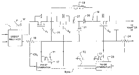
1o The Tnve"ti~m In an elechonic ballast in accordance with the
invention, as shown in Fig. 3, the arrangement is essentially the same as in
the
prior art ballast shown in Fig. 1 except for one important difference. To this
extent, identical components in the two electronic ballasts are referenced by
the
same abbreviations and reference numerals. In the ballast shown in Fig. 3, PFC
is stage 12, SC stage 13 and PC stage 14 included in the Fig. 1 ballast are
now
merged into a single circuit having fewer magnetic and power components than
those entailed by separate stages.
Thus the combined PFC, SC and PC stages in Fig. 3 include only three
MOSFET transistors functioning as electronic switches Sl, S2 and S3. Switch S1
2o carries out the PFC function of the ballast, switch S2 can-ies out both SC
and PC
functions while switch S3 is reserved for PC power control.
A MOSFET is a metal-oxide, field effect semiconductor characterized by
high switching speeds. Since in the ballast circuit the electronic switches
S1, S2
and S3 are synchronously activated by high-frequency control pulses whose
25 frequency can be as high as SOI~IiZ and higher, it is essential that the
switches be
capable of switching on and off at a very high rate.
In a typical arrangement in accordance with the invention, the pulsatory
DC output of bridge rectifier 11 whose waveform W is shown in Fig. 2 is
applied
to the electronic switch S 1 of a power factor correction circuit. Tlus switch
is
3o actuated by high-frequency square-wave pulses T1 produced by a pulse
generator
CA 02465829 2004-05-05
WO 03/041456 PCT/IBO1/02067
--7-
17, which thus serves as means for periodically activating the switch S 1.
Tlus
pulse generator as well as other pulse generators included in the ballast
circuit,
may be constituted by integrated circuit chips.
The periodic square wave pulses T1 from generator 17 which are applied
s to the gate of the MOSFET electronic switch S1 and act to turn the switch on
and
off at a high-frequency rate, are pulse width-modulated in accordance with a
control signal CSl derived from a series resistor 18 in the output of bridge
rectifier 11. Resistor 18, through which flows the input current to the power
factor correction circuit, acts as an input current sensor, and therefore
senses the
to displacement in phase of this current from the voltage.
Pulse width-modulation of the square wave pulses T1 applied to the gate
of MOSFET electronic switch Sl varies the duty cycle of the switching action,
that is the ratio of the ON time of the switch to its OFF time. Since the duty
cycle
is varied as a function of the degree and direction in which the input current
is
1s displaced in time phase from the voltage, switch S1 serves to bring about a
power
factor correction of the pulsatory DC power passing through this switch.
The power factor corrected, pulsatory DC power in the output of
electronic switch Sl is fed unidirectionally through a chore 19 in series with
a
diode 20 to storage capacitor 21 of a capacitor charge and discharge circuit,
the
2o capacitor being charged by the pulsatory DC wave W Choke 19 functions as a
low pass filter whose useful output is a direct current, as in a power supply
rectifier filter.
The storage capacitor circuit acts to modulate the pulsatory DC power
applied thereto by effectively filling in the valley V in the pulsatory wave W
This
2s action is carried out by the MOSFET electronic switch S2 which when pulse-
activated provides a discharge path through a diode 22, the discharge of
capacitor
21 then flowing unidirectionally through diode 22 in series with electronic
switch
S2 and choke 19 to a node N at the output of the capacitor circuit. Thus
capacitor
21 charges through diode 20 when switch S3 is active yet in an off state and
3o when switch S2 is closed, it then discharges through diode 22. Switch S2 is
open
CA 02465829 2004-05-05
WO 03/041456 PCT/IBO1/02067
_g-
when the input voltage is above the RMS value and is pulse-activated when the
voltage falls below this value. The voltage of capacitor 21 must be higher
than
the voltage supplied to the inverter.
The activation of electronic switch S2 is controlled to bring about a
s discharge in the internal represented by valley V in tile pulsatory DC wave
W
when the wave as shown in Fig. 2 is below the RMS level, thereby effectively
redistributing the available DC power.
To effect this action, electronic switch S2 is activated by high-frequency
square wave pulses T2 produced by a pulse generator 23, which thus serves as
1o means for periodically activating the switch S2. Pulses T2 are pulse-width
modulated by a control signal applied to the generator, this signal being
derived
from a resistor 24 in a series with the output line through which the load
current
flows. Hence resistor 24 acts as a load current sensor to provide a control
signal
that varies with variations in the load current. As a consequence, the duty
cycle of
1s electronic switch S2 is controlled whereby the discharge of the charged
storage
capacitor 21 acts to regulate the DC power yielded at the output node N of the
storage capacitor circuit.
The high-frequency pulse generators 17 and 23 operate in synchronism
with each other and when the switches S 1 and S2 periodically activated by
these
zo generators are both open, then current is supplied to chore 19 by a free-
wheeling
diode 25.
Power from node N is applied to the inverter 15 of the ballast system
through a power control circuit that includes a third electronic MOSFET switch
S3 to whose gate is applied pulse-width modulated control pulses T3 derived
2s from the pulse generator 23, which thus serves as means for periodically
activating the switch S3. Pulse width modulation of the control pulses T3 is
effected by a control signal derived from load current sensor 24. Switch S3 is
closed and conductive when the voltage applied thereto is below the RMS value,
and switch S2 executes simultaneously pulse-width modulation control. When the
CA 02465829 2004-05-05
WO 03/041456 PCT/IBO1/02067
-9-
voltage is above the RMS value, then switch S3 is activated to execute pulse-
width production control of the inverter, switch S2 then being open and
inactive.
Thus should the load current decrease to reflect a reduction in the power
applied to the HID lamp, the resultant control signal would cause an increase
in
s the width of pulses T3, when the input voltage is below the RMS level, with
a
resultant increase in the duty cycle of switch S2, when the input voltage is
below
the RMS level, thereby causing the load current to resume its proper intensity
The ballast circuit shown in Fig. 3 can-ies out the same function as the
PFC stage 12, the SC storage capacitor stage 13 and the PC power control stage
l0 14 in the prior art electronic ballast shown in Fig. 1. But it tales fewer
magnetic
and power components to do so, for the main components of the ballast circuit
in
accordance with the invention are three MOSFETs, a storage capacitor, a chore
and three diodes, there being no hansformer or other cumbersome parts. It
therefore becomes possible to manufacture a highly compact and light weight
1s electronic ballast unit for an HID lamp in which the magnetic and power
components of the ballast are fewer in number and smaller than those included
in
a conventional ballast and therefore can be packaged and potted in a small
casing.
As noted, in the ballast circuit shown in Fig. 3, the means for periodically
activating the MOSFETs S2 and S3 are served by a common pulse generator 23.
2o However, separate pulse generators may also be employed if desired.
Fig. 4 shows a ballast that is identical in construction and operation to the
ballast described above with reference to Fig. 3 apart from the inclusion of a
third
pulse generator 26 for feeding the pulses S3 to the MOSFET S3 in sync with the
pulses S2 fed by the second pulse generator 23 to the second MOSFET S2.
25 While there has been shown a prefeiTed embodiment of an electronic
ballast in accordance with the invention, it is to be understood that changes
may
be made therein without departing from the scope of the invention as defined
by
the claims.
Thus, when an electronic ballast in accordance with the invention is
3o designed to operate a DC powered HID lamp, it will then not include an
inverter
CA 02465829 2004-05-05
WO 03/041456 PCT/IBO1/02067
- 10-
to supply AC to an ignites as in Fig. 1. The ignites to be included in an
electronic
ballast for a DC powered HID lamp must be one appropriate to this DC lamp.
Moreover, an RFI filter for the AC supply, as shown in Fig. 1, is not
essential to
an electronic ballast in accordance with the invention.