Note : Les descriptions sont présentées dans la langue officielle dans laquelle elles ont été soumises.
CA 02477727 2007-11-07
77326-101
MEASURING CURRENT THROUGH AN ELECTRICAL
CONDUCTOR
TECHNICAL FIELD
This application relates to measuring current through an electrical conductor.
BACKGROUND
Coils such as Rogowski coils are used to measure current through an electrical
conductor.
SUMMARY
In one general aspect, a coil includes a first portion, a second portion, a
third
portion, and a fourth portion. The first portion is wound in a first direction
around a
first core and the second portion is wound in the first direction around a
second core.
The third portion is wound in a second direction that is different from the
first
direction around a third core such that the third portion is decoupled froin
the first and
second portions. Additionally, the fourth portion is wound in the second
direction
around a fourth core and decoupled from the first and second portions. An
inner area is
fonned by arranging the portions such that the first portion mates with the
second
portion and the third portion mates with the fourth portion. A voltage is
induced in
the coil if au electrical conductor is placed in the inner area
Implementations may include one or more of the following features. For
2o example the first and third portions may be connected at a first connection
point, the
third and fourth portions may be connected at a second connection point, and
the
fourth and second portions may be connected at a third connection point. In
this case,
the voltage induced in the coil may be measured across the first and second
portions
of the coil. Alternatively, the first and second portions may be connected at
a fourth
connection point and the voltage induced in the coil may be measared across
the
second connection point and the fourth connection point.
The first portion may be traced on a first printed circuit board that forms
the
first core and the second portion may be traced on a second printed circuit
board that
forms the second core. Likewise, the third portion may be traced on a third
printed
1
CA 02477727 2004-08-26
WO 03/073118 PCT/US03/05622
circuit board that forms the third core and the fourtll portion may be traced
on a fourth
printed circuit board that forms the fourth core. The first and second printed
circuit
boards may be laminated with the third and fourth printed circuit boards.
The first and second portions may mate to form a first loop and the third and
fourth portions mate to form a second loop. Thus, the first and second loops
may
define the inner area. The first and second loops may be rectangular,
circular, or
elliptical.
The first direction may be clockwise and the second direction may be
counterclockwise. The first, second, third, and fourth cores may be non-
magnetic.
The coil may include a fifth portion wound in the first direction around a
fifth
core and a sixth portion wound in the second direction around a six'th core.
In this
case, the inner area is formed by arranging the portions such that the first,
second, and
fifth portions mate with each other and the third, fourtll, and sixth portions
mate with
each other. The first, second, and fifth portions may mate to form a first
loop and the
third, fourth, and sixth portions mate to form a second loop.
The coil may be implemented in a system that includes a voltage measuring
device that measures a voltage induced in the coil when an electrical
conductor is
placed in the inner area. The system may also include a current calculating
device
connected to the voltage measuring device and configured to calculate the
current
through the electrical conductor based on the measured voltage.
Aspects of the techniques and systems can include one or more of the
following advantages. The coil exliibits improved current measurement accuracy
because each of the portions are identically and separately wound and then
located
near each other. Thus, the coil can better account for effects of fields not
produced by
the electrical conductor. Additionally, the improved current measurement
accuracy
results from the reduction of unwanted influence due to external
electromagnetic
fields and due to internal electromagnetic fields. In particular, influence
due to
external fields was measured in tests to be less than or equal to 0.2% and
influence
due to internal fields was measured in tests to be less than or equal to 0.6%.
Moreover, the accuracy of the coil matches or exceeds the accuracy of a high-
2
CA 02477727 2008-11-21
77326-101
precision laboratory current transformer, which is used for
measuring current through an electrical conductor.
The coil may be made of any shape and size because
it is made of portions that may be joined together to
accommodate any size electrical conductor. Each of the
first and second loops of the coil may be made of any
suitable number of portions, such as, for example, three or
four portions. Additionally, the shape of the coil may be
adjusted by adjusting the shape of each of the portions that
make up the first and second loops. One of the portions
that forms a loop may have a shape that is different from
the shape of the other portion that forms that loop. In
this way, an asymmetrical coil may be formed.
According to one particular aspect of the
invention, there is provided a measuring system comprising:
a coil comprising: a first portion wound in a first
direction around a first core; a second portion wound in the
first direction around a second core; a third portion wound
in a second direction around a third core and decoupled from
the first and second portions, the second direction being
different from the first direction; and a fourth portion
wound in the second direction around a fourth core, and
decoupled from the first and second portions; and a voltage
measuring device connected to both the first portion and the
second portion; in which the first and second portions mate
to form a first loop, the third and fourth portions mate to
form a second loop, the first and second loops define an
inner area that is configured to receive an electrical
conductor; in which a voltage is induced in the coil if an
electrical conductor is placed in the inner area; in which
the first and third portions are connected at a first
connection point, the third and fourth portions are
connected at a second connection point, and the fourth and
3
CA 02477727 2008-11-21
77326-101
second portions are connected at a third connection point;
in which the voltage measuring device measures a voltage
induced in the coil when an electrical conductor is placed
inside the inner area.
There is also provided a system for measuring a
current, the system including: a coil comprising: a first
loop including a first portion wound in a first direction
around a first core, and a second portion wound in the first
direction around a second core, the second portion coupling
with the first portion; and a second loop including a third
portion wound in a second direction around a third core and
decoupled from the first and second portions, the second
direction being different from the first direction, and a
fourth portion wound in the second direction around a fourth
core and decoupled from the first and second portions; in
which the first and second loops define an inner area that
is configured to receive an electrical conductor; and a
voltage measuring device that measures a voltage induced in
the coil when an electrical conductor is placed in the inner
area.
Another aspect of the invention provides a coil
comprising: a first loop including a first portion wound in
a first direction around a first core; and a second portion
wound in the first direction around a second core; and a
second loop including a third portion wound in a second
direction around a third core and decoupled from the first
and second portions, the second direction being different
from the first direction; and a fourth portion wound in the
second direction around a fourth core and decoupled from the
first and second portions; in which the first and second
loops define an inner area that is configured to receive an
electrical conductor.
3a
CA 02477727 2008-11-21
77326-101
Other features and advantages will be apparent
from the description, the drawings, and the claims.
DESCRIPTION OF DRAWINGS
Fig. 1 is an illustration of a system for
measuring current through an electrical conductor.
Figs. 2A and 3A show prior designs for coils used
in the system of Fig. 1.
Figs. 2B and 3B are circuit diagrams of the coil
designs of Figs. 2A and 3A, respectively.
Figs. 4A and 5A show designs for coils used in the
system of Fig. 1.
Figs. 4B and 5B are circuit diagrams of the coil
designs of Figs. 4A and 5A, respectively.
Fig. 6 shows a perspective view of a design for a
coil used in the system of Fig. 1.
Figs. 7A and 7B show detailed sections of the coil
design of Fig. 6.
Like reference symbols in the various drawings
indicate like elements.
DETAILED DESCRIPTION
Referring to Fig. 1, a system 100 is used to
measure a current through an electrical conductor 105. The
system 100 includes a coil 110 and a voltage measuring
3b
CA 02477727 2004-08-26
WO 03/073118 PCT/US03/05622
device 115 connected to the coi1110. The voltage measuring device 115 measures
a
voltage induced in the coil when the electrical conductor 105 is placed within
the coil
110. The current through the electrical conductor 105 may then be calculated
based
on the measured voltage. To this end, the system 100 may also include a
current
calculating device 120, which may be a computer. The current calculating
device 120
is connected to the voltage measuring device 115 to calculate the current
tllrough the
electrical conductor based on the voltage measured by the voltage measuring
device
115. Altllough shown separately from the voltage measuring device 115 in Fig.
1, the
current calculating device 120 may be integral with the voltage measuring
device 115.
The coil 110 includes a conductive eleinent that is wound around a non-
magnetic core. The conductive element may be, for example, a metal wire or a
metal
deposit. The non-magnetic core may be made of any material that has a magnetic
permeability that is equal to the permeability of free space. For example, the
non-
magnetic core may be an air core. As another example, the coil 110 may be a
Rogowski coil in which the non-magnetic core is a printed circuit board (PCB)
on
which the conductive element is traced. The PCB may be made of an epoxy resin
filled with a substance having a low coefficient of thermal expansion such as
glass or
ceramic.
Referring to Fig. 2A, a prior system includes a two-arm coi1210 having two
2o arms 215, 220 that form a main loop when coupled together for receiving an
electrical
conductor 205. The two arms 215, 220 are configured such that the conductive
element of the coil 110 winds around a non-magnetic core (not shown).
The coi1210 includes a return loop 225 that serves to reduce the influence of
nearby conductors carrying high currents by canceling electrical fields coming
from
outside the coi1210. The return loop 225 may be formed by returning the
conductive
element through the center of the two-arm winding (as shown in Fig. 2A).
Alternatively, the return loop may be formed by winding the conductive element
around the non-magnetic core in a direction opposite from the winding of the
main
loop.
4
CA 02477727 2004-08-26
WO 03/073118 PCT/US03/05622
A block diagram of the coi1210 is also shown in Fig. 2B with a representation
of the non-magnetic core 230. As can be seen in Figs. 2A and 2B, the main
loop,
wliich is made of arms 215, 220, and the return loop 225 are formed or
interwoven on
the same core 230. When the two loops are interwoven in this manner, they are
referred to as being "coupled" together. The voltage induced in the coil 210
is
measured across the arms 215, 220 in a series configuration.
Referring to Fig. 3A, another prior system includes a two-arm coil 310 having
two arms 315, 320 that form a main loop when coupled together for receiving an
electrical conductor 305. The two arms 315, 320 are configured such that the
conductive element of the coil 110 winds around the non-magnetic core (not
shown).
The coi1310 includes a return loop 325 that serves to reduce the influence of
nearby conductors carrying high currents by canceling electrical fields coming
from
outside the coi1310. The return loop 325 may be foniled by returning the
conductive
element through the center of the two-arm winding (as shown in Fig. 3A).
Alternatively, the return loop may be formed by winding the conductive element
around the non-magnetic core in a direction opposite from the winding of the
main
loop.
A block diagram of the coil 310 is shown in Fig. 3B with a representation of
the non-magnetic core 330. As can be seen from Figs. 3A and 3B, the main loop,
which is made of arms 315, 320, and the return loop 325 are formed on the same
core
330 and are therefore coupled together. The voltage induced in the coil 310 is
measured across a midpoint of the return loop 325 and a connection point
between the
two arms 315, 320 in a parallel configuration.
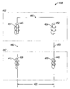
Referring to Figs. 4A and 4B, another design includes a two-arm coi1410 for
receiving an electrical conductor 405. The coi1410 includes a first portion
415, a
second portion 420, a third portion 427, and a fourth portion 428. The first
portion
415 is wound in a first direction around a first core 435 (represented in Fig.
4B) and
the second portion 420 is wound in the first direction around a second core
440
(represented in Fig. 4B). The first direction may be a clockwise or a
counterclockwise direction.
5
CA 02477727 2004-08-26
WO 03/073118 PCT/US03/05622
The third portion 427 is wound in a second direction around a third core 445
(represented in Fig. 4B), which is distinct from the first or second cores
435, 440.
The third portion 427 is not interwoven with and does not overlap the first or
second
portions 415, 420. When a portion is not interwoven with another portion, the
portions are referred to as being "decoupled" from one anotlier. Thus, the
third
portion 427 is decoupled from the first and second portions 415, 420.
Moreover, the
second direction is different from the first direction. Thus, if the first
direction is
clockwise, then the second direction is counterclockwise, and if the first
direction is
counterclockwise, then the second direction is clockwise.
The fourth portion 428 is wound in the second direction around a fourth core
450 (represented in Fig. 4B). Like the third portion 427, the fourth portion
428 is
decoupled from the first and second portions 415, 420.
When the portions 415, 420, 427, and 428 are arranged, the first portion 415
mates with the second portion 420 to form a first loop 442 and the third
portion 427
mates with the fourth portion 428 to form a second loop 452. In this
arrangement, an
inner area 455 is formed within the first and second loops 442, 452.,
respectively, for
receiving the electrical conductor 405. The first and third portions 415, 427
are
connected at a first connection point 460; the third and fourth portions 427,
428 are
connected at a second connection point 465; and the fourth and second portions
428,
2o 420 are connected at a third connection point 470. The voltage induced in
the coil
410 is measured across the first and second portions 415, 420 of the coil to
fonn a
series-connection configuration.
Referring to Figs. 5A and 5B, another design includes a two-arm coi1510 for
receiving an electrical conductor 505. Like coi1410, the coil 510 includes a
first
portion 515, a second portion 520, a third portion 527, and a fourth portion
528. The
first portion 515 is wound in a first direction around a first core 535
(represented in
Fig. 5B) and the second portion 520 is wound in the first direction around a
second
core 540 (represented in Fig. 5B). The first direction may be clockwise or
counterclockwise.
6
CA 02477727 2004-08-26
WO 03/073118 PCT/US03/05622
The third portion 527 is wound in a second direction around a third core 545
(represented in Fig. 4B), which is distinct from the first or second cores
535, 540. In
this way, the third portion 527 is decoupled from the first or second portions
515, 520.
Furthermore, the second direction is different from the first directiQn. Thus,
if the
first direction is clockwise, then the second direction is counterclockwise.
Alternatively, if the first direction is counterclockwise, then the second
direction is
clockwise. The fourth portion 528 is wound in the second direction around a
fourth
core 550 (represented in Fig. 5B). The fourth portion 528 is decoupled from
the first
and second portions 515, 520.
When the portions 515, 520, 527, and 528 are arranged, the first portion 515
mates with the second portion 520 to form a first loop 542 and the third
portion 527
mates with the fourth portion 528 to form a second loop 552 (as shown in Fig.
5A).
In this arrangement, an inner area 555 is formed within the first and second
loops for
receiving the electrical conductor 505. The first and third portions 515, 527
are
connected at a first connection point 560 and the third and fourth portions
527, 528
are connected at a second connection point 565. Additionally, the fourth and
second
portions 528, 520 are connected at a third connection point 570 and the first
and
second portions 515, 520 are connected at a fourth connection point 575. The
voltage
induced in the coil 510 is measured across the second connection point 565 and
the
fourth connection point 575 to form a parallel-connection configuration.
Referring also to Fig. 6, in one implementation, the coil 410 or 510 may be
formed as a Rogowski coil 610 for receiving an electrical conductor 605. In
coil 610,
the conductive element in each of the portions is traced on a respective PCB
core. In
particular, the coil 610 includes a first portion 615 that is traced in a
first direction on
a first PCB core 635 and a second portion 620 that is traced in the first
direction on a
second PCB core 640. The first direction may be clockwise or counterclockwise.
The coil 610 also includes a third portion 627 that is traced in a second
direction on a
third PCB core 645 and a fourth portion 628 that is traced in the second
direction on a
fourth PCB core 650. The third and fourth PCB cores 645, 650 are' distinct
from
either of the first or second PCB cores 635, 640. In this way, the third
portion 627
and the fourth portion 628 are decoupled from the first and second portions
615, 620.
7
CA 02477727 2004-08-26
WO 03/073118 PCT/US03/05622
Moreover, the second direction is different from the first direction. Thus, if
the first
direction is clockwise, then the second direction is counterclockwise, and if
the first
direction is counterclockwise, then the second direction is clockwise.
Each of the PCB cores is formed as a thinly shaped piece defined by two
opposing surfaces. The conductive element of the coil 610 is traced onto the
PCB
core by depositing a metal (such as, for example, copper) onto each of the
surfaces of
the PCB. As shown, the metal deposits are rectilinear and radial, depending on
their
location on the PCB, and form a rectangular/elliptical shape. Other shapes may
be
formed, including, for example, circular, triangular, or rectangular shapes.
In
1o particular, the metal deposits may be all radial, with geometric
projections
intersecting at a center of the coil, to form a circular coil (not shown).
Alternatively,
the metal deposits may be all rectilinear to form a rectangular coil (not
shown).
When the portions 615, 620, 627, and 628 are arranged, the first portion 615
mates with the second portion 620 to form a first loop 642 and the third
portion 627
mates with the fourth portion 628 to form a second loop 652. In this
arrangeinent, an
inner area 655 is formed within the first and second loops 642, 652,
respectively, for
receiving the electrical conductor 605.
The first and third portions 615, 627 are connected at a first connection
point
660 and the third and fourth portions 627, 628 are connected at a second
coimection
point 665. The fourth and second portions 628, 620 are connected at a third
connection point 670. The voltage induced in the coi1610 is measured across
the first
and second portions 615, 620 of the coi1610 in a series configuration.
Fig. 7A shows a section 700 of the portion 615 or 620. Metal deposits on a
surface of the PCB core 635 or 640 that is visible to the reader are shown as
a
continuous line 710 and metal deposits on the opposite surface of the PCB core
that is
not visible to the reader are shown as a dashed line 715. The portion 615 or
620 is
traced in a counter-clockwise direction. Metal deposits on a surface of the
PCB core
are connected to metal deposits on the opposite surface of the PCB core
through
conductively plated holes 720, referred to as vias, passing through the PCB
core.
Connections to the portion 615 or 620 are made with plated connection pads,
one of
8
CA 02477727 2004-08-26
WO 03/073118 PCT/US03/05622
which is shown and labeled 722. For example, one connection pad on the portion
615
connects to a connection pad on the portion 627 at the first connection point
660 and
the other connection pad on the portion 615 connects to the voltage measuring
device
115. As another example, one connection pad on the portion 620 connects to a
connection pad on the portion 628 at the third connection point 670 and the
other
coimection pad on the portion 620 connects to the voltage measuring device
115.
Fig. 7B shows a section 705 of the portion 627 or 628. Metal deposits on a
surface of the PCB core 645 or 650 that is visible to the reader are shown as
a
continuous line 730 and metal deposits on the opposite surface of the PCB core
that is
1o not visible to the reader are shown as a dashed line 735. The portion 627
or 628 is
traced in a clockwise direction. Metal deposits on a surface of the PCB core
are
connected to metal deposits on the opposite surface of the PCB core through
vias 740
passing through the PCB core. Connections to the portion 627 or 628 are made
with
plated connection pads, one of which is shown and labeled 744. Thus, as
mentioned
above, one connection pad on the portion 627 connects to a connection pad on
the
portion 615 at the first coimection point 660, and the other connection pad on
the
portion 628 connects to a connection pad on the portion 620 at the third
connection
point 670. Additionally, another connection pad on the portion 627 connects to
a
connection pad on the portion 628 at the second connection point 665.
In general, the first and second loops in a coi1410, 510, or 610 are arranged
to
permit connection at the connection points and are positioned relative to each
other at
any suitable distance. For example, the distance that separates the first and
second
loops may depend on the required measurement precision for the coil.
Other implementations are within the scope of the following claims.
For example, the Rogowski coil may be designed with a higher density in
which a number of traces per unit length is increased by offsetting the vias
in, for
example, a radial direction. In this way, each of the portions includes two
sets of
conductive elements traced on the PCB core. Both of the sets progress in one
direction.
9
CA 02477727 2004-08-26
WO 03/073118 PCT/US03/05622
The coil may be designed with more than two layers of loops. The current
measuring system may be used to measure current in each phase of a multi-phase
circuit. For example, if the circuit is a three-phase circuit, then the
current measuring
system includes three coils, one for each phase.
The first and second loops 642, 652 may be laminated together to form a
monolithic PCB assembly. Such an assembly protects and insulates the coil from
moisture and electromagnetic shorts. The current measuring system may include
an
electronic measurement and/or acquisition circuit. The voltage measuring
device 115
may perform integration on the measured voltage to produce a voltage that is
proportional to current. To perform integration, the device 115 may include an
RC
integrator or an operational amplifier.
The coil may be made of any shape and size. For example, each of the first
and second loops of the coil may be made of any suitable number of portions,
such as,
for example, three or four portions. Additionally, the shape of the coil may
be
adjusted by adjusting the shape of each of the portions that make up the first
and
second loops. One of the portions that forms a loop may have a shape that is
different
from the shape of the other portion that forms that loop. In this way, an
asymmetrical
coil may be formed.