Note : Les descriptions sont présentées dans la langue officielle dans laquelle elles ont été soumises.
CA 02481194 2004-09-10
TITLE OF THE INVENTION
Terminal Structure of Superconducting Cable and Superconducting Cable Line
Therewith
BACKGROUND OF THE >NVENTION
Field of the Invention
The present invention relates generally to terminal structures of
superconducting cables including a cable core having a supercor~ducting layer,
and
superconducting cable lines including the terminal structure, and particularly
to terminal
structures of superconducting cables helping to attach a ground wire to the
superconducting layer while preventing an electrical insulation layer from
having
impaired insulating property, and lines including the terminal structure.
Description of the Background Art
As one of superconducting cables that have been produced using a
superconductor layer formed of a Bi-based high-temperature superconducting
tape for
example, not only a single phase cable including a single cable core but a
multiphase
superconducting cable of multicore type that is produced by assembling a
plurality of
cable cores into one unit is also under development.
Referring to Fig. 5, this superconducting cable 100 includes three cable cores
102 twisted and housed in a thermal insulation pipe 101. Thermal insulation
pipe 101
has an outer pipe 101 a and an inner pipe 101b. This double pipe constructed
of these
outer pipe lOla and inner pipe lOlb has a thermal insulai:ion material (not
shown
provided therein and a vacuum is produced within the double pipe.
These cable cores 102 each include, in the order starting from the innermost
component, a former 200, a superconductor layer 201, an electrical insulation
layer 202,
a superconducting shield layer 203, and a protection layer 204. Superconductor
layer
201 is constructed by winding superconducting wires around former 200 in a
spiral
manner in layers. Electrical insulation layer 202 is formed of wound
insulation paper
formed of polypropylene and kraft paper in lamination. Superconducting shield
layer
-1-
CA 02481194 2004-09-10
203 is constructed by winding superconducting wires similar to that of
superconductor
layer 201 around electrical insulation layer 202 in a spiral manner. In this
superconducting shield layer 203, in a steady state, a current is induced of
substantially
the same magnitude as and opposite in direction to a current flowing through
superconductor layer 201. The induced current creates. a magnetic field, which
can
cancel out a magnetic field generated from superconductor layer 201 and thus
there is
substantially no magnetic field leaking outside cable core 102. A space 103
formed
between inner pipe 101b and each cable core 102 normally provides a path where
a
refrigerant flows. Thermal insulation pipe 101 has a radially outer portion
provided
with an anticorrosion layer 104 of polyvinyl chloride:
For normal conducting multiphase cables, by contrast, it is known that
normally
each cable core has a shield layer grounded to obtain a ground potential for
each phase.
This technique is described for example in Power Cable Technology Handbook,
New
Edition by Kihachiro Iizuka, Kabushiki Kaisha Denkishoin, March 25, 1989,
first edition,
first copy, p.645. The shield layer is grounded by directly attaching a ground
wire to
the shield layer and grounding the wire, connecting the wire to a grounded
construction.
The ground wire is often attached to the shield layer by bonding using typical
solder
having a melting point of approximately 190°C, compression-bonding, or
the like.
A superconducting cable also requires having a superconducting shield layer
processed, and grounding the superconducting shield layer is desired. If the
superconducting cable has the superconducting shield layer grounded in the
manner
employed to ground a normal conducting cable's shield layer, however, a
problem arises:
First, a superconducting layer is formed of a superconducting ~rire which does
not have
a mechanical strength that can endure compression bonding. As such, such
compression molding as employed for normal conducting cables ca~onot be
employed.
If the superconducting cable has the superconducting shield layer with a
ground wire
attached thereto by using the above-described, typical solder, which has a
melting point
higher than the temperature limit of the electrical insulation layer
underlying the
CA 02481194 2004-09-10
superconducting shield layer, the heat applied to melt the solder impairs the
electrical
insulation layer's insulating property.
Furthermore, directly attaching a ground wire to the superconducting shield
layer of the superconducting cable may damage a superconducting wire
configuring the
superconducting shield layer and impair the electrically insulation layer's
insulating
property, as described above. Accordingly, rather than directly attaching a
ground
wire to a superconducting shield layer, indirectly attaching the ground wire
to the
superconducting shield layer is desired.
SL>TvLMARY OF THE lI~'VENTION
A main object of the present invention is to provide a terminal structure of a
superconducting cable allowing a superconducting layer to be grounded without
impaired characteristic of the superconducting layer, a superconducting shield
layer, in
particular, and impaired insulating property of an electrical insulation
layer, and a
superconducting cable line including the terminal structure. Another object of
the
present invention is to provide a terminal structure of a superconducting
cable in a
multiphase cable that has a superconducting shield layer appropriately
processed to pass
an induced current, and a superconducting cable line including the terminal
structure.
The present invention achieves the above objects by arranging a connection
electrode at a radially outer portion of a superconducting layer and also
connecting the
superconducting layer and the connection electrode with a solder having a low
melting
point.
More specifically the present invention is a terminal structure of a
superconducting cable including a cable core having a superconducting layer
and an
electrical insulation layer that further includes a connection electrode
arranged at an
radially outer portion of the superconducting layer and the connection
electrode and the
superconducting layer are connected with a low melting solder. Furthermore
when the
superconducting layer is a superconductor layer and a superconducting shield
layer the
connection electrode is arranged at a radially outer portion of the
superconducting shield
CA 02481194 2004-09-10
layer and the connection electrode has a ground wire attached thereto.
Furthermore
when the superconducting cable is a multiphase cable including a plurality of
cable cores
the connection electrode is arranged at a radially outer portion of a super
conducting
shield layer of each cable core and such connection electrodes are linked by a
conductive
coupling member.
In accordance with the present invention a superconducting cable has a
superconducting layer having a radially outer portion provided with a
conductive
connection member (a connection electrode) fixed to the superconducting layer
by
employing a low melting solder to prevent an electrical insulation layer from
having
impaired insulating property associated with attaching the connection member.
The
connection electrode can have a ground wire previously attached thereto, and
the
electrode with the wire can be attached to the superconducting layer, the
superconducting shield layer, in particular, to eliminate the necessity of
directly attaching
the ground wire to the superconducting shield layer. Tlus can prevent the
I5 superconducting shield layer from damage associated with attaching the
ground wire
and also prevent the electrical insulation layer from having impaired
insulating property.
Furthermore, if the superconducting cable is a multiphase cable including a
plurality of cable cores, each cable core may have a superconducting shield
layer having
a radially outer portion provided with a connection electrode and the
superconducting
shield layer and the connection electrode may be connected with a low melting
solder;
and each superconducting shield layer may be grounded. The present inventors
have
studied the same and as a result have found that when each cable core has the
superconducting shield layer grounded a problem arises, as follows: a
superconducting
cable passes a significantly larger current than a normal conducting cable. If
each cable
core has its superconducting shield layer grounded via the earth, each cable
core may
disadvantageously have the superconducting shield layer connected via the
earth. If
such is done, the superconducting shield layer, large in connection
resistance, passes a
current smaller in magnitude than that flowing through a superconductor layer.
Thus
CA 02481194 2004-09-10
each cable core's superconducting shield layer cannot create a magnetic field
that can
cancel a magnetic field generated from each cable core's superconductor layer
and a
large magnetic field is generated external to each cable core. Accordingly in
the
present invention cable cores have their respective superconducting shield
layers having
radially outer portions, respectively, provided with connection electrodes,
respectively,
connected together by a conductive coupling member to reduce connection
electrode
and short circuit the superconducting shield layers. A magnetic field that can
cancel a
magnetic field generated from each cable core's superconductor layer can be
generated
at each superconducting shield layer. A magnetic field leaking from each cable
core
can thus be reduced.
Hereinafter the present invention will be described more specifically.
The present invention is directed to a superconducting cable including a cable
core having a superconducting layer and an electrical insulation layer. As
such, it may
be a single phase cable including a single cable core as described above, or a
multiphase
cable including a plurality of cable cores as described above. The multiphase
cable
includes a 3-phase superconducting cable having three cable cores twisted
together and
accommodated in a thermal insulation pipe. The cable may be any of known
superconducting cables.
The superconducting layer includes a superconductor layer and a
superconducting shield layer. It is recommended that these superconducting
layers be
formed by helically winding a wire formed of a Bi2223-base superconducting
material
and they may be provided in a single layer or multiple layers. For the
multiple layers,
insulation paper formed of polypropylene and kraft paper in lamination is
wound
between the layers to provide an insulation layer. Furthermore between the
superconductor layer and the superconducting shield layer an electrical
insulation layer
is interposed. It is recommended that the electrical insulation layer be
formed by
winding PPLP~ or similar insulation paper formed of polypropylene and kraft
paper in
lamination. Furthermore in the present invention the superconductor layer has
a
-5-
CA 02481194 2004-09-10
radially outer portion provided with a connection electrode and the
superconductor
layer and the connection electrode are bonded together with a low melting
solder.
Solder has a melting point varying depending on its chemical composition. In
the present invention is used a low melting solder, a solder having a melting
point lower
than typically used solder having a melting point of approximately
190°C (hereinafter
simply referred to as "the typical solder"). More specifically, a solder
having a melting
point lower than the electrical insulation layer's temperature limit, is used.
The
electrical insulation layer is formed of PPLP~ or similar insulation paper
formed of
polypropylene and kraft paper in lamination having a temperature limit of
approximately
130°C. That is, the typical solder, having a melting point higher than
the electrical
insulation layer's temperature limit, would invite impaired insulating
property of the
electrical insulation layer. Accordingly to prevent the electrical insulation
layer from
having impaired insulating property a solder having a melting point of less
than 130°C,
more preferably at most 120°C, is used. On the other hand, a solder is
desired that
does not melt and also has a level of mechanical strength for a range from a
normal
temperature to an extremely low temperature at which the cable is cooled by
refrigerant.
Solder having such properties includes that having a melting point of at least
60°C.
Such low-melting solder may be commercially available solder.
Furthermore in attaching the connection electrode a temperature sensor can be
~0 attached for example on the electrical insulation layer, the
superconducting shield layer
and/or the like to confirm each layer's temperature to better prevent the
electrical
insulation layer from having impaired insulating property. The temperature
sensor
includes a thermocouple or the like. It is recommended that the temperature
sensor be
attached with tape, solder or the like, and removed after the connection
electrode is
attached with the low melting solder at a radially outer portion of the
superconducting
layer.
The connection electrode is used to link a ground wire, superconducting layers
together, and/or the like. It is recommended that such connection electrode be
formed
_6_
CA 02481194 2004-09-10
of conductive material such as copper, aluminum (both having a specific
resistance p at
77K = 2 X 10-~52~ cm) or similar metal having a small electrical resistance at
a
refrigerant's temperature at which the superconducting cable is used, e.g.,
around liquid
nitrogen's temperature when liquid nitrogen is used as refrigerant. The
connection
electrode preferably has a geometry contacting at least a portion of the
superconducting
layer as seen circumferentially. If the superconducting layer is formed of a
plurality of
superconducting wires, in particular, the connection electrode preferably has
a geometry
capable of electrically connecting all the constituent superconducting wires
together.
For example it includes a cylinder capable of covering th;e superconducting
layer's outer
circumference entirely. If the connection electrode is a cylinder, it is
preferably formed
of pieces arcuate in cross section combined together to form the cylinder to
help to
attach the connection electrode to the superconducting layer
circumferentially. More
specifically, pieces each having a semi-circular, arcuate geometry in cross
section
combined together are included in the connection electrode.
The connection electrode preferably has a ground wire connected thereto and
by attaching the ground wire-attached connection electrode to the
superconducting layer
at a radially outer portion the superconducting layer, the superconducting
shield layer in
particular, can be prevented from damage associated wii:h attaching the ground
wire and
the electrical insulation layer can be prevented from having impaired
insulating property.
Furthermore, employing the ground wire-attached connection electrode can
facilitate
grounding the superconducting shield layer. The ground wire is attached to the
connection electrode with solder or a bolt or by means of compression
connection or
similar mechanical connection. In the present invention the superconducting
layer has
a ground wire attached thereto via the connection electrode. Accordingly, such
mechanical connection as described above can also be employed, and the ground
wire
can be readily and reliably attached. Furthermore, the connection electrode
can be
attached to the superconducting cable at any desired location, providing
excellent
workability. Furthermore, for multiphase cables, an increased degree of
freedom can
7-
CA 02481194 2004-09-10
be provided in selecting a location at which connection electrodes are linked.
For a multiphase cable including a plurality of cable cores, it is recommended
that the cable cores have their respective superconducting layers, their
superconducting
shield layers in particular, provided with connection electrodes, as described
above,
respectively, and these connection electrodes be linked by a conductive
coupling
member to short circuit the superconducting shield layers, and a ground wire
attached to
the connection electrode associated with any of the cable cores can be
grounded to
ground the plurality of cable cares collectively. Note that it is sufficient
to provide the
ground wire-attached connection electrode to any single one of the cable
cores. The
other cable cores may be provided with ground wire-free connection electrodes,
respectively.
The connection electrode and the coupling member are connected, for example
for a 3-phase superconducting cable including three cable cores, by the so-
called Y
connection. More specifically, the cable cores have radially outer portions,
respectively,
I5 provided with their respective connection electrodes, wr~ich have their
respective
coupling members attached thereto, each at one end, and the coupling members
have
their respective other ends connected toward the center of the triangle having
the
connection electrodes as apexes. Alternatively, the so-called ~1 connection is
also
considered. More specifically, the cable cores have radially outer portions,
respectively,
provided with their respective connection electrodes, which serve as apexes
and
coupling members link the connection electrodes such that the coupling members
correspond to sides linking the apexes (or connection electrodes). For the Y
connection the coupling members may have their respective other ends connected
by
employing a separate, center electrode to connect the coupling members'
respective
other ends to the center electrode.
The coupling member is preferably formed of flexible material. More
specifically, it includes a material formed of a braided material for example.
Such a
flexible coupling member allows following the movement of the cable core as it
is
_g_
CA 02481194 2004-09-10
cooled and contracts. As the cable core contracts, tension is caused. The
tension is,
however, exerted mainly on the flexible coupling member and hardly exerted on
the low
melting solder having a tendency to have mechanical strength smaller than the
above
described typical solder. A.s such, the low melting solder's portion can
effectively be
protected. Furthermore, if the present terminal structure corresponding to a
multiphase cable is accommodated in a splitter box, the flexible coupling
member can
contribute to excellent workability in linking the connection electrode in the
splitter box,
which has a limited space, and also absorb a dimensional error, such as
positional offset,
distortion and the like, introduced as the electrode is linked. If such a
flexible coupling
member is used and for example the connection electrode is connected in the
above
described Y connection; the coupling member may be attached so that that
portion of
the connection electrode at which the coupling member is attached and the
portion (or
the center electrode) connecting such coupling members together have the same
position
as seen along the cable cores, although offsetting the portions as seen along
the cores
I5 can help to attach the coupling member.
It is recommended that the connection electrode be attached such that the
protection layer is removed and the superconducting layer; the superconducting
shield
layer in particular, is exposed. In doing so, to more ef~Fectively prevent the
electrical
insulation layer from having impaired insulating property, it is preferable
that the
connection electrode and the electrical insulation layer are thermally
insulated. For
example a tape, a sheet or the like formed of thermally insulating material is
wound
between the superconducting shield layer and the electrical insulation layer.
The
thermally insulating material includes glass, fiber reinforced plastic (FRP)
and the Like.
If the superconducting shield layer has multiple layers, and each layer has a
connection
electrode connected thereto at a portion having a difFerent axial length,
connection
resistance may vary and a biased current distribution may be invited.
Accordingly it is
desired that the axial length be equal. Accordingly if the superconducting
shield layer
is multiple layers, each layer may be stepwise stripped at a portion connected
to the
-9-
CA 02481194 2004-09-10
connection electrode and an innermost layer (a layer located most adjacent to
the
electrical insulation layer) is cut to equalize the innermost layer's axial
length and the
other, stepwise strip layers' axial length to partially expose the electrical
insulation layer.
Preferably, the exposed electrical insulation layer has a circumference with
the above
mentioned, thermally insulating tape or the like wound therearound and the
connection
electrode is attached. Furthermore, the exposed electrical insulation layer
may also
have a temperature sensor attached thereon to confirm the layer's temperature
when
low-melting solder is used to attach the connection electrode to the
superconducting
layer at a radially outer portion.
The present terminal structure is applied in a sL~perconducting cable line for
example at a connection linking a superconducting cable and a normal
conducting cable
together, a connection linking a superconducting cables together or a portion
provided
with a termination structure such that the terminal structure is provided to a
superconducting cable at opposite terminals. Such portions are portions at
which a
cable terminal is processed to form a connection structure, a termination
structure or the
like and the connection electrode can be readily arranged.
For a multiphase cable including a plurality of cable cores, the connection
structure, termination structure and the like as described above are formed by
splitting
for each phase, i.e., for each cable core. The split cable cores are housed in
a splitter
box. More specifically, the multiphase cable's cores assembled at an assembly
portion
are spaced increasingly as they extend therefrom, and th.e cable cores are
thus housed in
the sputter box. The splitter box has a thermal insulation structure to be
filled with
liquid nitrogen or similar refrigerant to cool the cores.
Each cable core protruding from the box is provided with a thermal insulation
pipe filled with liquid nitrogen or similar refrigerant to maintain a
superconducting state
similarly as maintained in the box. Accordingly, attaching a connection
electrode to a
superconducting shield layer of each cable core protruding from the splitter
box will
significantly be cumbersome. The connection electrode may be attached to a
- 10-
CA 02481194 2004-09-10
superconducting layer of each cable core extracted from the splitter box.
Preferably,
however, that the connection electrode is attached to the cable core internal
to the
sputter box as such allows superior workability in attaching the electrode.
It is recommended that in the sputter box each cable core be held by a holding
tool. The holding tool includes that capable of holding each cable core and
also
holding cable cores such that they are spaced. In particular, a holding tool
is preferable
that has a configuration capable of moving in the splitter box as the cable
core expands
and contracts.
Furthermore for multiphase cables the superconducting layer, the
superconducting shield layer in particular, is preferably grounded only at one
end of
cable terminal and not grounded at the other end of the cable terminal, since
for
superconducting cables, grounding at opposite terminals may form a closed loop
via the
earth and connect superconducting shield layers together via the earth.
Thus, as has been described above, in the present superconducting cable's
terminal structure a cable core can have a superconducting layer having a
radially outer
portion provided with a connection electrode having a ground wire attached
thereto to
effectively prevent the superconducting layer from damage associated with
attaching the
ground wire and prevent an electrical insulation layer from impaired
insulating property.
Furthermore, for multiphase cables, connection electrodes can be linked
together to
short circuit superconducting shield layers. As such, each cable core's
superconducting
shield layer can create a magnetic field canceling a magnetic field generated
from each
superconductor layer, and a large magnetic field generated external to each
cable core
can be prevented. In particular, in the present invention, the superconducting
layer and
the connection electrode can be connected with low-melting solder, and
attaching the
connection electrode does not impair the electrical insulation layer's
insulating property.
The foregoing and other objects, features, aspects and advantages of the
present invention will become more apparent from the following detailed
description of
the present invention when taken in conjunction with the accompanying
drawings.
-11-
CA 02481194 2004-09-10
BRIEF DESCRIPTION OF THE DRAWINGS
Fig. 1 schematically shows a terminal structure of a superconducting cable in
accordance with the present invention.
Fig. 2A schematically shows a configuration of a connection electrode arranged
to surround a superconducting shield layer and Fig. 2B is a partially notched
view
showing the connection electrode arranged at a portion of a cable core on a
superconducting shield layer at a radiaily outer portion.
Fig. 3 is a schematic cross section showing how the connection electrode and a
coupling member are connected in the Y connection.
Fig. 4 is a schematic cross section showing how the connection electrode and
the coupling member are connected in the D connection.
Fig. 5 is a cross section of a 3-phase superconducting cable using three cores
collectively.
DESCRIPTION OF THE PREFERRED EMBODIMENTS
Hereinafter the present invention in embodiment will be described.
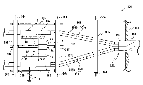
Fig. 1 shows a superconducting cable line 300 including a terminal structure
of
a superconducting cable 100. The superconducting cable 100 terminal structure
is a
terminal structure of a multiphase superconducting cable including a plurality
of cable
cores 102 having a superconducting layer and an electrical insulation layer,
and each
cable core 102 has the superconducting layer (in the present embodiment, a
superconducting shield layer) surrounded by a connection electrode 1. The
superconducting shield layer and connection electrode 1 are connected with a
low-melting solder. In the present embodiment 3-phase superconducting cable
100
including three cable cores 102 will be used as an example for description.
The present embodiment employs 3-phase superconducting cable 100, which is
similar in configuration to that shown in Fig. 5. More specifically, as seen
radially
outwards, cable core 102 includes former 200, a superconductor layer 201, an
electrical
insulation layer 202, a superconducting shield layer 203 and a protection
layer 204.
-12-
CA 02481194 2004-09-10
For 3-phase superconducting cable l00 three cable cores 102 are twisted
together and
accommodated in a thermal insulation pipe 101. Former 200 is constructed by
twisting
a plurality of copper wires each coated with an insulator. Superconductor
layer 201
and superconducting shield layer 203 are constructed by winding in a spiral
manner a
Bi2223-based superconducting tape-shaped wire (Ag-Mn sheath wire) in layers
around
former 200 and electrical insulation Layer 202, respectively. Electrical
insulation layer
202 is constructed by winding insulation paper formed of polypropylene and
kraft paper
in lamination (polypropylene laminated paper (PPLP~) manufactured by Sumitomo
Electric Industries, Ltd.) around superconductor layer 201. Protection layer
204 is
constructed by winding kraft paper around superconductirlg shield layer 203.
Thermal
insulation pipe 101 is an SUS corrugated pipe. Between an outer pipe lOla and
an
inner pipe lOlb an insulator is arranged in layers. Pipes lOla and lOlb form a
double
pipe, which is internally vacuumed. More specifically, thermal insulation pipe
101 has
a vacuumed, multilayered, thermal insulation structure. Thermal insulation
pipe l0I
has a radially outer portion provided with an anticorrosion layer 104 of
polyvinyl
chloride.
The above described 3-phase superconducting cable 100 is twisted and thus
accommodated in thermal insulation pipe 101 and at the terminal portion cable
cores
102 are spaced and thus split, and accommodated in a splitter box 300. Cable
cores
102 thus split have their respective superconducting shield layers provided
with
connection electrodes 1, respectively, at a radially outer portion, and
connection
electrodes 1 are connected to a conductive, coupling member 2 to electrically
connect
the superconducting shield layers together, or short-circuit the layers.
With reference to Figs. 2A and 2B, connection electrode 1 includes a
semi-circular, arcuate pieces la and lb, as seen in cross section, combined
together to
provide a cylindrical geometry. Pieces la and lb have opening edges provided
with
flanges 1 c, respectively, extending along connection electrode 1. Pieces 1 a
and 1 b
have their respective flanges 1 c faced to each other, receiving and passing a
bolt or
-I3-
CA 02481194 2004-09-10
similar fixture through a hole (not shown) and clamped together by screwing a
nut to
form the cylindrical geometry. One piece 1 a has a fixture I d to which
coupling
member 2, described hereinafter, is connected, and a hole Ie introducing low-
melting
solder between connection electrode I and the superconducting shield layer.
While in
the present embodiment two holes 1 a are shown by way of example, a single
hole 1 a
may be provided. In the present embodiment connection electrode 1 is formed of
copper.
Connection electrode 1 is attached such that cable core I02 has protection
layer 204 removed to expose superconducting shield layer 203. In the present
embodiment superconducting shield layer 203 is configured of the two layers of
inner
and outer layers 203a and 203b. Accordingly it is recommended that the layer
be
stripped stepwise so that a superconducting wire configuring each layer 203a,
203b can
contact low-melting solder 5.
Furthermore, connection electrode I not only short circuits superconducting
shield layers 203 but may also have a ground wire 3 attached thereto. In the
present
embodiment piece Ib has ground wire 3 attached thereto, as shown in Figs. 2A
and 2B.
Alternatively, piece 1 a may have the ground wire attached thereto. Ground
wire 3 can
be attached with typical solder.
With reference to Fig. l, in the present embodiment, coupling member 2 is
formed of a braided material of copper. Furthermore, in the present
embodiment,
connection electrode 1 and coupling member 2 are connected by Y connection,
and
coupling members 2 are connected together by a separately prepared center
electrode 4.
In the present embodiment, fixture 1 d and center electrode 4 are positionally
offset as
seen lengthwise, and coupling member 2 has one end connected to fixture 1 d
and the
other end connected to center electrode 4 so that coupling member 2 is
arranged along
cable care 102.
Center electrode 4 is formed of a conductive material (in the present
embodiment, copper) and includes a ring 4a at the center and an attachment 4b
arranged
- 14-
CA 02481194 2004-09-10
on ring 4a circumferentially at equal intervals to connect coupling member 2.
A long
bolt 305 fixed between first and second holding tools 301b and 302b holding
cable core
I02, as will be described later, is inserted into ring 4a and center electrode
4 is fixed to
long bolt 305. As such when the cable is cooled and cable 102 accordingly
contracts
moves, contact electrode 1 and center electrode 4 can follow the movement of
core 102
as coupling member 2 flexes and expands in a fixed condition. Furthermore, a
large
portion of tension caused as cable core 102 contracts is exerted on coupling
member 2,
which is flexible, and the low melting solder hardly experiences tension.
Connection
electrode 1 can thus be prevented from being removed from superconducting
shield
layer 203 as cable core 102 expands and contracts.
Connection electrode I is arranged on superconducting shield layer 203 at a
radially outer portion in a procedure, as will be described hereinafter with
reference to
Figs. 2, and 2A and ZB. At a terminal portion of a superconducting cable,
cable cores
I02 are split and each cable core 102 at a portion provided with connection
electrode 1
Z5 has a protection layer removed therefrom to expose superconducting shield
layer 203.
In the present embodiment, the cable core is stripped stepwise to allow
superconducting
shield layer 203 to have inner and outer layers 203a and 203b both exposed and
an
interlayer insulation layer (a layer formed by a wound electrical insulation
paper) present
between inner and outer layers 203a and 203b is removed. Furthermore in the
present
embodiment inner layer 203a is cut to expose a portion of electrical
insulation layer 202
so that inner layer 203a at a portion connected to connection electrode I has
an axial
length equal to outer layer 203b. The exposed superconducting shield layer 203
and
electrical insulation layer 202 may have a thermocouple attached thereon to
confirm
each layer's temperature.
The exposed electrical insulation layer 202 preferably has a radially outer
portion provided with a thermal insulation layer 6 to prevent impaired
insulating
property attributed to heat transmitted while soldering. Thermal insulation
layer 6 is
formed for example of glass fiber cloth tape. Furthermore, if superconducting
shield
-15-
CA 02481194 2004-09-10
layer 203 has a portion to which low-melting solder 5 is not applied, it is
recommended
that the portion be masked. If layer 203 has a portion to which solder 5 is
applied, the
portion is preferably solder-plated to help low-melting solder 5 to adhere to
the portion.
Furthermore, solder-plating may be facilitated for example by polishing or
washing a
surface of the superconducting shield layer. The layer may be solder plated
while each
layer's temperature is confirmed via the thermocouple.
Connection electrode 1 is arranged on superconducting shield layer 203 at a
radially outer portion. Connection electrode 1 passes an electric current to
superconducting shield layer 203 at fixture ld. Accordingly, a portion closer
to fixture
1 d is smaller in connection resistance. As such in a superconducting tape
line
configuring the superconducting shield layer 203 inner and outer layers 203a
and 203b a
wire closer to fixture ld is smaller in connection resistance and a wire
farther from
fixture 1 d is larger in connection resistance. In other words, inner and
outer layers
203a and 203b are both vary in circumferential connection resistance depending
on
location relative to fixture ld. Accordingly in the present embodiment, as
shown in Fig.
2B, connection electrode 1 is arranged to connect connection electrode I and
superconducting shield layer 203 as remote as possible from fixture 1 d, as
shown in Fig.
2B. Furthermore in the present embodiment pieces 1a and 1b are arranged to
cover
superconducting shield layer 203 and pieces la a.nd lb have their flanges Ic
facing each
other and clamped with a bolt to fix connection electrode 1 on supercondueting
shield
layer 203 at radially outer portion. In doing so, hole 1 a formed in
connection electrode
1 to introduce the low melting solder may have a thermocouple attached in a
vicinity
thereof by means of tape or the like to confirm the temperature of connection
electrode
1. Furthermore, a gasket may be interposed or heat resistive tape may be wound
or a
similar sealing may be provided to prevent the low melting solder from leaking
from the
two opposite pieces la and Ib between their flanges lc and connection
electrode 1 at its
opposite ends. The gasket arranged between flanges I c includes a sheet of
silver, a
sheet of indium or other similar soft material. The heat resistive tape
includes glass
-16-
CA 02481194 2004-09-10
tape and the like.
The low melting solder is introduced through hole I e. In doing so, a heating
means is required for placing the solder in liquid phase. If the heating means
is a
burner, a soldering iron or the like, connection electrode 1 would have a
local portion
heated to high temperature and electrical insulation layer 22 underlying that
portion may
have its insulating property unpaired. Accordingly, a heater is used as the
heating
means and attached to cover connection electrode 1 at a radially outer
portion.
Connection electrode 1 can thus uniformly be heated. Desirably in introducing
the low
melting solder the thermocouple is monitored and the heater's output is
adjusted to
IO prevent electrical insulation layer 202 from having a temperature exceeding
130°C,
preferably to set a temperature of 120°C or less. In the present
embodiment the low
melting solder is a solder having a melting point of approximately 78°C
(with a chemical
composition of 9.3% by mass of Sn, 34.5% by mass of P'b, 50% by mass of Bi,
and
6.2% by mass of Cd). After the solder is introduced, the thermocouple, the
sealing and
the like are removed. Thus a structure with connection electrode 1 and
superconducting shield layer 203 connected with the low melting solder can be
provided.
After cable cores 102 are provided with connection electrodes 1 on
superconducting shield layers 203 at radially outer portions, respectively,
connection
electrodes 1 are linked together by coupling member 2 to short circuit
superconducting
shield layer 203. More specifically, coupling member 2 has one end connected
to
connection electrode 1 at fixture 1 d by a bolt and the other end connected to
center
electrode 4 at attachment 4b by a bolt. Cable cores 102 can thus have their
respective
superconducting shield layers 203 short-circuited together.
For the 3-phase superconducting cable described in the present embodiment
one of three cable cores 102 is provided with connection electrode 1 having
ground wire
3 previously attached thereto. As three cable cores 1'02 have their respective
superconducting shield layers 203 short-circuited by connection electrode 1,
coupling
-17_
CA 02481194 2004-09-10
member 2 and center electrode 4, grounding ground wire :3 can ground the three
cable
core I02 superconducting shield layers 203 collectively. Preferably, the Fig.
1 terminal
structure is provided at opposite ends of superconducting cable 100 and the
cable is
grounded only at one end so that cable cores 102 will not have superconducting
shield
layers 203 connected via earth.
In the present terminal structure a connection electrode can be arranged on a
superconducting shield layer at a radially outer portion and have a ground
wire attached
thereto to prevent the superconducting shield layer from damage associated
with
attaching the ground wire and prevent an electrical insulation layer
underlying the
superconducting shield layer from having impaired insulating property. In
particular, as
the connection electrode and the superconducting shield layer can be connected
with
low melting solder, the electrical insulation layer can effectively be
prevented from
having impaired insulating property associated with attaching the connection
electrode.
Furthermore, the connection electrode and the conductive coupling member that
link
cable cores' respective superconducting shield layers provide short circuit
between the
superconducting shield layers when the cable has a current flowing
therethrough. In
other words, in the present invention, superconducting shield layers are
connected with
small interconnection resistance, and a current flowing Through each
superconducting
shield layer can substantially be equalized in magnitude to that flowing
through each
superconductor layer, respectively. As such, a magnetic field sufficient to
cancel a
magnetic field generated from each superconductor Layer can be created to
prevent a
large magnetic field generated external to each cable core. Furthermore, the
superconducting shield layers short-circuited can be grounded collectively and
hence
efficiently.
Note that the portion of cable core 102 split and provided with connection
electrode 1 is accommodated in a splitter box 300. Splitter box 300
accommodates
three cable cores 102 such that they axe increasingly spaced. Furthermore,
sputter box
300 preferably has a heat insulation structure as it is filled with liquid
nitrogen or similar
-18-
CA 02481194 2004-09-10
refrigerant to cool core 102 accommodated therein. In the present embodiment
splitter
box 300 has a cylindrical geometry. Ground wire 3 attached to connection
electrode 1
is extracted from sputter box 300 and grounded. It is recommended that Ground
wire
3 and splitter box 300 be hermetically sealed to maintain hermeticity.
Cable cores 102 accommodated in splitter box 300 extend from one side box of
300 (or an assembly portion of core 102, shown in Fig. I at the right hand)
toward the
other side of box 300 (or a split termination of core 102, as seen in Fig. 1
at the left
hand) such that cable cores 102 are increasingly spaced and they held with a
fixed
distance therebetween. In the Fig. 1 example, a first holding tool 301a
holding the
assembly portion, a first holding tool 301b holding an intermediate portion, a
second
holding tool 302 holding the split termination, and an intermediate holding
tool 303
holding cable core 102 between the first holding tools 301a and 301b hold
cable core
102.
The first holding tool 30Ia has a center provided with an annular portion.
The annular portion has an outer circumference with equally spaced, three
intermediate
holding tools 303 and a member in the form of a sector., arranged between
intermediate
holding tools 303, fixed thereto. The first holding tool 30Ia is arranged
between core
102 so as to position the annular portion's center substantially at the center
of the space
surrounded by the three cable cores I02 and by arranging cable cores 102 at
intermediate holding tools 303, respectively, cable cores 102 axe spaced and
thus held.
In the present embodiment a sliding portion 304 substantially point-contacting
an inner
surface of box 300 is provided to the sector member so that the first holding
tools 301 a
can also move within box 300 as cable core 102 expands and contracts. The
first
holding tool 301b is basically similar in configuration to the first holding
tool 303a,
except that the former has an annular portion larger in diameter than the
latter. The
first holding tools 301 a and 301b are linked by intermediate holding tool
303.
The second holding tool 302 is substantially similar in configuration to the
first
holding tool 301b. The first and second holding tools 30Ib and 302 are linked
by a
- 19-
CA 02481194 2004-09-10
plurality of long bolts and held with a fixed spacing therebetween.
Furthermore, the
first and second holding tools 301b and 302 each have an annular portion
provided with
a cylindrical insulation member 307 formed ofFRP or similar insulation
material and
receiving long bolt 305.
Intermediate holding tool 303 includes an elongate, semi-circular, arcuate or
canaliculate member 303a fixed to the first holding tools 301x, 301b annular
portion at a
radially outer portion, and a plurality of short, semi-circular, arcuate
member 303b
combined with canaliculated member 303a to surround cable core 102
circumferentially
to form a cylinder. In the present embodiment member 303a and members 303b are
first arranged on cable core 102 at a radially outer portion which is then
clamped with a
band (not shown) or similar clamping member far fixture on cable core 102 at
the
radially outer portion to hold the core. Intermediate holding tool 303 may be
provided
with a through hole, as appropriate, to help cable core 102 accommodated
therein to
contact a refrigerant.
In the Fig. 1 example, the connection electrode is attached at a split
termination
having cable cores sufficiently spaced. The connection electrode can be
readily and
hence efficiently attached.
In the Fig. 1 configuration, center electrode 4 and the connection electrode 1
fixture 1 d are positionally offset as seen lengthwise. Alternatively, as
shown in Fig. 3,
connection electrode 1 and center electrode 4 may have fixture 1 d and
attachment 4b,
respectively, set at a single position and fixture ld and attachment 4b may be
linked by
coupling member 2 in the Y connection. More specifically, fixture 1 d of each
of three
connection electrodes 1 arranged on cable cores 102 at radially outer
portions,
respectively, and attachment 4b connected to center electrode 4 at ring 4a may
be
arranged opposite and linked by coupling member 2. Alternatively, as shown in
Fig. 4;
the center electrode may be dispensed with, and pieces la and 1b each having
fixture ld
connected thereto or only one of which has two fixtures 1 d connected thereto
may be
used to allow a connection electrode 1 and another connection electrode 1 to
have their
-20-
CA 02481194 2004-09-10
respective fixtures 1 d linked by coupling member 2 to provide the D
connection. In
other words, three coupling members 2 may form the three sides of a triangle
having
apexes corresponding to three connection electrodes 1 arranged on cable cores
10~ at
radially outer portions, respectively.
The present terminal structure is suitable for constructing a terminal portion
of
a superconducting cable. Furthermore the present terminal structure is also
suitable for
constructing a superconducting cable line including such a terminal structure.
Although the present invention has been described and illustrated in detail,
it is
clearly understood that the same is by way of illustration and example only
and is not to
be taken by way of limitation, the spirit and scope of the present invention
being limited
only by the terms of the appended claims.
-21 -