Note : Les descriptions sont présentées dans la langue officielle dans laquelle elles ont été soumises.
CA 02489898 2006-07-14
LOW LOSS AWG MULTIPLEXER
BACKGROUND OF THE INVENTION
1. FIELD OF THE INVENTION
The present invention relates to an optical coupler for
branching or coupling optical signals, a beam splitter for
branching optical signals, and an AWG (Arrayed Waveguide Grating
type optical wavelength division multiplexer) for combining or
branching optical signals. Particularly, the present invention
is concerned with an optical coupler, a beam splitter, and an
AWG, of a low loss type.
2. DESCRIPTION OF RELATED ART
With an increase of the information transmission volume,
a WDM (Wavelength Division Multiplexing) transmission system
capable of remarkably increasing the transmission capacity is
in wide commercial use. In this WDM transmission system, optical
signals of plural wavelengths are transmitted using a single
optical fiber. Therefore, optical wavelength division
multiplexers are needed at input and output portions of the
optical fiber which serves as a transmission path. The optical
wavelength division multiplexer combines optical signals of
plural wavelengths for transmitting them with use of a single
optical fiber or branches wavelength-division-multiplexed
optical signals transmitted using a single optical fiber into
respective wavelengths. An AWG(Arrayed Waveguide Gratingtype
optical wavelength division multiplexer) can perform optical
CA 02489898 2004-12-10
2
wavelength division multiplex/demultiplex at wavelength
intervals of the order of several tens of GHz to 100 GHz. For
this reason the AWG is in wide use as a key device in a WDM
transmission system.
In the AWG, wavelength-division-multiplexed optical
signals are inputted at an equal phase to arrayed waveguides
by means of a first slab waveguide. The thus-divided optical
signals of the same phase are given a phase difference by being
propagated through the arrayed waveguides of different optical
path lengths. Next, the optical signal thus given a phase
difference are inputted to a second slab waveguide. Within the
second slab waveguide, light condensing positions of the optical
signals are different wavelength by wavelength. Therefore, the
optical signals are divided into respective wavelengths and then
outputted by means of output waveguides disposed at light
condensing positions of corresponding wavelengths. It is
important for the AWG, as a passive part, to be as low as possible
in its optical signal propagation loss. Thus, the attainment
of a low loss is demanded.
One cause of loss peculiar to the AWG is that, when optical
signals are propagated from the slab waveguide to the arrayed
waveguides, a portion thereof leaks f rombetween adjacent arrayed
waveguides and is not incident on the arrayed waveguides. In
the connections between the arrayed waveguides and the slab
waveguide there occurs a loss of 1 to 2 dB (decibel) due to such
leakage of light. Methods for diminishing this loss have
heretofore been proposed, for example the method disclosed in
Japanese Unexamined Patent Publication No. 2000-147283
CA 02489898 2004-12-10
3
(paragraph 0013, FIG. 1). In this method, as the first
conventional example, tapered waveguides which is inclined in
a taperedmanner are formed at the position where light is inputted
from the slab waveguide to the arrayed waveguides.
FIG. 1 shows a principal portion of an AWG used in this
first conventional example. Wedge-like tapered waveguides 13
as buried layers are formed around connections between a slab
waveguide 11 and plural arrayed waveguides 121r 122, ..., 125, ...
in the AWG indicated at 10. The tapered waveguides 13 are formed
by etching. In the connections of the arrayed waveguides 121r
122, ..., 125r ... to the slab waveguide 11, the height of the
tapered waveguides 13 is almost equal tothat of the slab waveguide
11 and becomes smaller with separation from the slab waveguide
11.
Consequently, in the connections between the slab
waveguide 11 and the arrayed waveguides 121, 122, ..., 125, ...
in the AWG 10, an electromagnetic field distribution changes
gradually. Therefore, optical signals having been propagated
through the slab waveguide 11 are incident without leakage on
the connections with the arrayed waveguides 121, 122, ..., 125r ....
As a result, it is possible to attain a low loss. Reversibly,
optical signals having been propagated through the arrayed
waveguides 121r 122, ..., 125, ... can be incident on the slab
waveguide 11 at a low loss.
However, in forming the wedge-like tapered waveguides 13,
it is necessary that an inclination be formed by changing the
etched depth (height) gradually. Consequently, there arises
the problem that it is necessary to use such a special photomask
CA 02489898 2004-12-10
4
or etching method as causes a continuous change of light quantity.
Thus, an obstacle is encountered in the productivity of the
tapered waveguides 13. Further, the light propagation
characteristic greatly changes depending on the thickness of
the tapered waveguides 13 formed among the arrayed waveguides
121r 122, ..., 125, ... . It is therefore necessary to control
the inclination of each tapered waveguide 13 with a high accuracy.
Thus, a problem is encountered in point of reproducibility and
uniformity of the shape of the tapered waveguides 13.
In an effort to solve this problem there has been proposed
such a second method as in for example Japanese Unexamined Patent
Publication No. Hei 10(1998)-274719 (see paragraphs 0010 and
0012, FIGS. 1 and 2) in which mesh-like waveguides are formed
in connections between a slab waveguide and arrayed waveguides
to diminish an insertion loss.
FIG. 2 shows, for reference, a slab waveguide and the
vicinity thereof in an ordinary AWG, while FIG. 3 shows a slab
waveguide and the vicinity thereof in the second conventional
example referred to above. In the ordinary AWG 20 shown in FIG.
2, input waveguides 22 and output waveguides 23 are simply
connected to a slab waveguide 21.
On the other hand, in the AWG 30 of the second conventional
example shown in FIG. 3, input waveguides 32 are not specially
different from that shown in FIG. 2, output waveguides 33 have
a transition region 34 in the vicinity of their connections with
a slab waveguide 31. The transition region 34 is formed by plural
waveguide paths 35 extending across the output waveguides 33.
Although in the figure the waveguide paths 35 are shown in a
CA 02489898 2004-12-10
reduced number,actua11y20to40,preferably about 30, waveguide
paths 35 are present. The waveguide paths 35 are formed of the
same material as the material of the output waveguides 33.
Therefore, the waveguide paths 35 can be manufactured in the
5 same step as the step of manufacturing the slab waveguide 31
and the output waveguides 33 which constitute the AWG 30.' The
waveguide paths 35 are gradually smaller in width with separation
from the slab waveguide 31. This is because with separation
from the slab waveguide 31 the leakage of optical signals among
the output waveguides 33 decreases gradually, and is to decrease
the leakage through the waveguide paths 35 of optical signals
under propagation through the output waveguides 33.
Consequently, optical signals under propagation among the output
waveguides 33 can be picked up into the output waveguides 33
effectively by the waveguide paths 35. In the AWG 30 of this
second conventional example, the insertion loss can be decreased
by the presence of the transition region 34. As an example,
in a typical star coupler, the insertion loss can be decreased
from about 0.8 dB to about 0.3 dB.
However, in the AWG 30 of the second conventional example,
periodic changes in refractive index occur in the connections
between the output waveguides 33 and the waveguide paths 35
extending across the output waveguides. As a result, optical
signals of a specific wavelength are accumulated and appear as
reflection. This reflection causes ripple, cross talk, and
distortion, in the optical wavelength division
multiplex/demultiplex characteristic of the optical wavelength
division multiplexer and thus exerts a bad influence thereon.
CA 02489898 2004-12-10
6
SUMMARY OF THE INVENTION
According to the present invention there are provided an
optical coupler, a beam splitter, and an AWG, which are provided
with a transition region for attaining a low loss and which can
effectively prevent the reflection of optical signals occurring
in the transition region.
The optical coupler according to the present invention
comprises a slab waveguide, one or more input waveguides for
inputting optical signals to the slab waveguide, plural output
waveguides for outputting optical signals from the slab
waveguides, and plural waveguide paths for connecting adjacent
ones of the output waveguides. The waveguide paths adjacent
to each other with respect to each of the output waveguides a4e
positioned at mutually different distances from the slab
waveguide.
Thus, the optical coupler according to the present
invention is provided with waveguide paths for connecting
adjacent output waveguides through which optical signals are
outputted. The waveguide paths are arranged in such a manner
that the waveguide paths positioned on the right and left sides
of each of the output waveguides are different in their distances
fromtheslab waveguide. Consequently, in each output waveguide,
a rise in equivalent refractive index caused by an arrangement
of the waveguide paths is decreased and reflection becomes
difficult to occur.
The beam splitter according to the present invention
comprises an input waveguide, plural output waveguides connected
CA 02489898 2004-12-10
7
to the input waveguide to output optical signals, and plural
waveguide paths for connecting adjacent ones of the output
waveguides. The waveguide paths adjacent to each other with
respect to each of the output waveguides are positioned at
mutually different distances from the input waveguide.
Thus, the beam splitter according to the present invention
is provided with waveguide paths for connecting adjacent output
waveguides through which optical signals are outputted. The
waveguide paths are arranged in such a manner that the waveguide
paths positioned on the right and left sides of each of the output
waveguides are different in their distances from the input
waveguide. Consequently, in each output waveguide, a rise in
equivalent refractive index caused by an arrangement of the
waveguide paths is decreased and reflection becomes difficult
to occur.
The arrayed waveguide grating type optical waveguide
division multiplexer according to the present invention
comprises one or more input waveguides for the input of optical
signals, a first slab waveguide coupled to the input waveguides
to branch the optical signals, plural arrayed waveguides coupled
to another side of the first slab waveguide to impart a phase
difference to each of the optical signals, a second slab waveguide
coupled to another side of the arrayed waveguides to branch and
output the optical signals, plural output waveguides coupled
to another side of the second slab waveguide to output the optical
signals, and waveguide paths for connecting adjacent ones of
the arrayed waveguides, the waveguide paths being positioned
near one or both of the first and second slab waveguides. The
CA 02489898 2004-12-10
8
waveguide paths adjacent to each other with respect to each of
the arrayed waveguides are positioned at mutually different
distances from the first or the second slab waveguide.
Thus, the arrayed waveguide grating type optical
wavelength division multiplexer according to the present
invention is provided with waveguide paths for connecting
adjacent ones of arrayed waveguides in which optical signals
are outputted from the first slab waveguide. The waveguide paths
are arranged in such a manner that the waveguide paths positioned
on the right and left sides of each output waveguide are mutually
different in their distances from the first or the second slab
waveguide. Consequently, in each output waveguide, a rise in
equivalent refractive index caused by an arrangement of the
waveguide paths is decreased and reflection becomes difficult
to occur.
The waveguide paths may satisfy the following conditions.
(1) The waveguide paths connect adjacent output waveguides
or arrayed waveguides alternately right and left.
(2) Adjacent waveguide paths are dislocated from each other
in the longitudinal direction of output waveguides or arrayed
waveguides.
(3) The waveguide paths are arranged at random intervals in
the longitudinal direction of output waveguides.
(4) The waveguide paths are arranged at gradually longer
intervals in the longitudinal direction of output waveguides
or arrayed waveguides.
(5) The waveguide paths become thinner with separation from
a slab waveguide or an input waveguide.
CA 02489898 2004-12-10
9
(6) The waveguide paths are arranged so as to be inlined with
respect to output waveguides or arrayed waveguides..
(7) The waveguide paths are different in width between output
waveguides or arrayed waveguides to which the waveguide paths
are connected.
BRIEF DESCRIPTION OF THE DRAWINGS
The above and other objects, features and advantages of
the present invention will become more apparent from the
following detailed description when taken in conjunction with
the accompanying drawings wherein:
FIG. 1 is a perspective view showing a principal portion
of an AWG (Arrayed Waveguide Grating type optical wavelength
division multiplexer) as a first conventional example;
FIG. 2 is a plan view showing a slab waveguide and the
vicinity thereof in a conventional ordinary AWG;
FIG. 3 is a plan view showing a slab waveguide and the
vicinity thereof in an AWG as a second conventional example;
FIG. 4 is a schematic construction diagram of an AWG
according to a first embodiment of the present invention;
FIG. 5 is an enlarged plan view of connections between
a first slab waveguide and arrayed waveguides shown in FIG. 4;
FIG. 6A is a construction diagram of a part of a transition
region in the AWG shown in FIG. 3, and FIG. 6B is an explanatory
diagram showing a change in refractive index thereof;
FIG. 7A is a construction diagram of a part of a transition
region in the AWG shown in FIG. 4, and FIG. 7B is an explanatory
diagram showing a change in refractive index thereof;
CA 02489898 2004-12-10
FIG. 8 is an enlarged plan view of connections between
a first slab waveguide and arrayed waveguides in a first
modification of the first embodiment;
FIG. 9 is an enlarged plan view showing a part of a transition
5 region in a second modification of the first embodiment;
FIG. 10 is an enlarged plan view showing a part of a
transition region in a third modification of the first
embodiment;
FIG. 11 is an enlarged plan view showing a part of a
10 transition region in a fourth modification of the first
embodiment;
FIG. 12 is an enlarged plan view showing a part of a
transition region in a fifth modification of the first
embodiment;
FIG. 13 is an enlarged plan view showing a part of a
transition region in a sixth modification of the first
embodiment;
FIG. 14 is an enlarged plan view of connections between
a first slab waveguide and arrayed waveguides in a seventh
modification of the first embodiment;
FIG. 15 is a plan view showing the construction of a beam
splitter according to a second embodiment of the present
invention;
FIG. 16 is a plan view showing the construction of a beam
splitter according to a first modification of the second
embodiment; and
FIG. 17 is a plan view showing the construction of a beam
splitter according to a second modification of the second
CA 02489898 2004-12-10
11
embodiment.
DETAILED DESCRIPTION OF THE PREFERRED EMBODIMENTS
Basic constructions of an optical coupler, a beamsplitter,
and an AWG, according to the present invention, as well as
operation principles thereof, will be described in detail
hereinbelow.
First, a description will be given of a basic construction
of an AWG (Arrayed Waveguide Grating type optical wavelength
division multiplexer) according to a first embodiment of the
present invention.
FIG. 4 shows an outline of the AWG of the first embodiment.
One or more first channel waveguides 52, plural second channel
waveguides 53, and arrayed waveguides 54 which are bent in certain
directions at different radii of curvature, are arranged on a
substrate 51 as a constituent of the AWG 50. A first slab
waveguide 55 for connection between the first channel waveguide
52 and the arrayedwaveguides 54, as well as a second slab waveguide
56 for connection between the arrayed waveguide 54 and the second
channel waveguides 53, are also arranged on the substrate 51.
A transition region 61 for gently changing the state of connection
i s provided near one or both of the f irst and second slab waveguides
55, 56. A certain optical path length. difference (waveguide
length difference) AL is provided between adjacent arrayed
waveguides 54. The optical path length is set so as to become
gradually longer or shorter.
Next, the following description is provided about a basic
operation of the AWG of this first embodiment.
CA 02489898 2004-12-10
12
Multiplexed optical signals of wavelengths X1, X2, ...
Xn inputted to the first channel waveguides 52 are expanded their
traveling path by the first slab waveguide 55 and are inputted
at an equal phase to the arrayed waveguides 54. The optical
signals thus inputted at an equal phase are each given a phase
difference of a certain interval by the arrayed waveguides 54
and reach the second slab waveguide 56. Since there actually
occurs wavelength dispersion, an isophase surf ace of each optical
signal is inclined by the wavelength. As a result, the optical
signals having been diffused by the second slab waveguide 56
have different light focusing (condensing) positions, depending
on wavelengths. Therefore, the second channel waveguides 53
are arranged on a boundary surface of the second slab waveguide
56 and at positions corresponding to wavelengths. Thus, optical
signals of wavelength components X1, X2, ...Xnare outputted each
individually from the second channel waveguides 53. A light
branching action and a light combining action are performed
reversibly, and in the case where optical signals of wavelength
components X1r X2, ... X,, are inputted each individually from
the second channel waveguides 53, multiplexed optical signals
of wavelengths X1, X2, ...kn are outputted from the first channel
waveguides 52.
The following description is now provided about the
construction of the AWG according to this first embodiment.
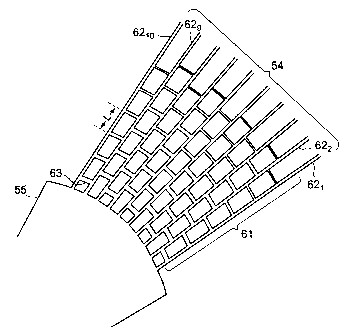
FIG. 5 concretely shows connections between thefirstslab
waveguide 55 and the arrayed waveguides 54. The arrayed
waveguides 54 are provided with a transition region 61 in the
vicinity of their connections with the first slab waveguide 55.
CA 02489898 2004-12-10
13
In the transition region 61, adjacent ones of waveguides 621r
622, ..., 6210r which constitute the arrayed waveguides 54 are
connected through waveguide paths 63. The number and
illustration of the waveguides are an example for explanation
and no limitation is made thereto.
The waveguide paths 63 used in this embodiment are of the
following structure.
The waveguide paths 63 are disposed on only one side at
connection points to the waveguides 621r- 622, ..., 6210.
Unlike the conventional example of FIG. 3, the waveguide paths
63 do not intersect the waveguides 621r 622, ..., 6210.
The waveguide paths 63 used in this embodiment may be
constructed as follows.
(1) In the transitiori region 61, the waveguide paths 63 are
arranged at equal intervals L in the longitudinal direction of
the waveguides 621r 622, . . ., 6210.
(2) The waveguide paths 63 may be arranged such that the
positions of connections between odd- and even-number waveguides
in the waveguides 621r 622, ..., 6210 are dislocated by L/2 in
the longitudinal direction. For example, the waveguide paths
63 which connect the waveguides 621 and 622 are dislocated by
L/2 from the waveguide paths 63 which connect the waveguides
622 and 623.
The length L is about several m to several ten m, e.g., 20
m. The height of cores which constitute the waveguides 621,
622, ..., 6210 and the waveguide paths 63 is in the range of about
several m to several ten pm, e. g. , 7 m. The core width of the
waveguides 621r 622, ..., 6210 is about several pm to several
CA 02489898 2004-12-10
14
ten m, e. g. , 7 m. The width of each waveguide path 63 is about
several m to 20 m, e.g., 7 m.
(3) Several to several ten waveguide paths 63 are provided
for each of the waveguides 621r 622, ..., 6210.
Further, following conditions may be added in this
embodiment.
(4) In the transition region 61, the close to the first slab
waveguide 55, the larger the thickness of each waveguide path
63. For example, the waveguide paths 63 are each about 18 m
wide at a position closest to the first slab waveguide 55 and
about 2 mwide at a position remotest from the first slab waveguide
55. This is because the closer to the first slab waveguide 55,
the larger the amount of optical signals picked up after leaking
between adjacent ones of the waveguides 612, 622, 624, ..., 6210.
(5) The waveguide paths 63 may be constituted by curved lines
which are concentric with a curved line defined by input ends
of the waveguides 621r 622, ..., 621o.
Under the above conditions, the reflection which occurs
in the transition region 34 provided in the second conventional
example shown in Fig.3 decreases remarkably in the transition
region 61 provided in this embodiment shown in Fig. 5. The reason
is described as follows.
FIG. 6 is an enlarged diagram of a part of a transition
region in the AWG of the second conventional example shown in
FIG, 3 and FIG. 7 is an enlarged diagram of a part of a transition
region in the AWG of this embodiment shown in FIG. 5.
A description will now be given of the AWG 30 of the second
conventional example with reference to FIGS. 6A and 6B.
CA 02489898 2004-12-10
FIG. 6A shows a waveguide pattern in a transition region.
Waveguide paths 351r 352, ... intersect an output waveguides
33n. A optical signal 82 travels in the direction of arrow 81
through the output waveguide 33n. FIG. 6B shows a change in
5 equivalent refractive index which the light traveling in the
direction of arrow 81 through the waveguide senses. Thus, in
the second conventional example, since waveguide paths are
arranged on both sides while intersecting the output waveguide,
there occurs a large change in equivalent refractive index. The
10 change in equivalent refractive index is repeated at every
distance L and with the same cycle. Therefore, out of slight
ref lected light portions which occur at intersecting points where
the waveguide paths 351r 352, ... intersect the output waveguide,
only those of a specific wavelength strengthen each other. As
15 a result, the reflection of the specific wavelength increases.
On the other hand, the AWG, indicated at 50, according
to this embodiment will be described below with reference to
FIGS. 7A and 7B.
FIG. 7A shows a waveguide pattern in a transition region.
Waveguide paths 631Rr 632R, 633R, 631L, 632L, and 633L, are dislocated
by L/2 with respect to an output waveguide 62õ and are connected
on only one side. A optical signal 84 travels in the direction
of arrow 83 through the output waveguide 62n. FIG. 7B shows
a change in equivalent refractive index which the light traveling
in the direction of arrow 83 through the waveguide senses. Thus,
in FIG. 7B, since the waveguide paths are arranged on only side,
there occurs only a relatively small change in equivalent
refractive index. Consequently, the reflection of the optical
CA 02489898 2004-12-10
16
signal by the waveguide paths 631R, 632R, 633R, 631L, 632L, 633L
becomes weaker. Thus, in this embodiment, a periodic change
in equivalent refractive index in the transition region 61 shown
in Fig. 5 is diminished to a large extent. As a result of such
a decrease of a periodic change in equivalent refractive index,
the reflection of a specific wavelength is decreased to a large
extent. Accordingly, the AWG 50 of this embodiment can afford
a satisfactory transmission characteristic.
Fig. 8 is an enlarged view of connections between the slab
waveguide 55 and the arrayed waveguides 54 in a firstmodification
of the first embodiment. Inthisfirstmodification,the arrayed
waveguides 54 comprising waveguides 621r 622, ..., 6210 are of
the same layout structure as in the first embodiment. In a
transition region 61A, adjacent ones of waveguides 621r 622,
...,
6210 which constitute the arrayed waveguides 54 are connected
together by waveguide paths 63A. The number and illustration
of the waveguides are an example for explanation and no limitation
is made thereto.
This first modification is the same as the first embodiment
with respect to the conditions (1) and (3) referred to in the
first embodiment, provided the condition (2) adopted therein
is different from that in the first embodiment.
(2) The positions where the waveguide paths 63A connect the
waveguides 621r 622, ..., 6210 are dislocated by L/3 between
adjacent waveguide paths. More specifically, waveguide paths
63A which connect the waveguides 624 and 623, waveguide paths
63A which connect the waveguides 623 and 622, and waveguide paths
63A which connect the waveguides 622 and 621r are dislocated
CA 02489898 2004-12-10
17
by L/3 from one another. The waveguide paths 63Amay be arranged
in a mutually L/3 dislocated manner in the direction opposite
to the illustrated direction.
Also in this first modification, the same conditions as
the conditions (4) and (5) in the first embodiment may be added.
In this first modification, the position where reflection
occurs by the waveguide paths 63A changes 2/3 cycle every time.
Therefore, the reflection of the wavelength which is amplified
with cycle L can be inhibited effectively as in the first
embodiment.
In the f irst embodiment the waveguide path 63 are arranged
at every L/2 interval, while in this first modification the
waveguide paths 63A are arranged atevery L/3 interval. However,
the mode of layout is not limited thereto. If n is assumed to
be a positive integer other than "1, " the waveguide paths may
be arranged at intervals of L/n.
As shown in FIG. 8, the waveguide paths 63A may be formed
by curved lines which are concentric with a curved line defined
by connected ends of the waveguides 621r 622, ..., 6210 where
the waveguides are connected to the slab waveguide 55.
FIG. 9 shows a part of a transition region in a second
modification ofthe first embodiment. In this transition region,
indicated at 61B, in the second modification, waveguide paths
63B arranged right and left of each of waveguides 621r 622, 623,
624, ... are mutually dislocated by AL (*0) . By thus arranging
the waveguide paths 63B so as not to be at equal intervals in
the longitudinal direction of the waveguides 621, 622, 623,
624, ..., it is possible to suppress the amplification of the
CA 02489898 2004-12-10
18
reflected wavelength as in the first modification.
Thus, in this second modification, the waveguide paths
63B are mutually dislocated by AL so as not to intersect the
waveguides 621, 622, 623, 629, ... . Consequently, the change
in equivalent refractiveindex which is sensed during propagation
of light is weakened. This construction of the second
modification is a more generalized construction of the first
embodiment shown in FIG. 5 or of the first modification shown
in FIG. 8.
FIG. 10 shows a part of a transition region in a third
modification ofthefirstembodiment. Inthe transition region,
indicated at61C,in thisthird modif ication, unlike the previous
...,
embodiment and modifications, layout intervals L1, L2, L3,
Ln (Ln is not shown) become longer gradually in the direction
away from the first slab waveguide 55 shown in FIG. 5 or FIG.
8. Three intervals L1r L2, and L3 shown in the figure are in
such a relation of magnitude as shown by the following expression
(1):
L1<L2<L3 . . . (1)
Thus, the layout intervals Ll, L2, L3, ..., Lr, of the
waveguide paths 63C are made longer with separation from the
first slab waveguide 55. This is because, in the optical signals
leaking out among the waveguides 621, 622, 623, 624, ..., 62n,
the amount of optical signals picked up becomes smaller as the
distance from the first slab waveguide 55 becomes longer. This
reason is common to the reason why the width of the waveguide
paths 61A is set so as to become smaller with separation from
the first slab waveguide 55. In this third modification, even
._.,
CA 02489898 2006-07-14
19
the waveguide paths 63C arranged between the same waveguides
are different in their intervals L1r L2, L3, ..., Lr,. Therefore,
the reflection of a specific frequency can be prevented more
effectively from being amplified.
In the constructions described above, the intervals of
waveguide paths have a certain regularity. However, even by
such waveguide paths where intervals have no regularity but merely
change at random, there can be obtained the same effects as above.
FIG. 11 shows a part of a transition region in a fourthmodification
of the first embodiment. In the transition region, indicated
at 61D, in this fourth modification, waveguide paths 63D are
arranged at random intervals L1, L2, L3, ....
L1#L2r L2#L3, L1#L3 ... (2)
With this layout, in the longitudinal direction of
waveguides 621r 622, 623, 624, ..., the reflection-occurring
wavelength can be changed at random, whereby it is possible to
prevent the occurrence of a periodic reflection of optical
signals and hence possible to diminish accumulation of the
reflection of specific wavelength optical signals.
FIG. 12 shows a part of a transition region in a fifth
modification ofthe first embodiment. Inthe transition region,
indicated at 61E, in this fifth modification, waveguide paths
63E which connect mutually adjacent waveguides 621 and 622, 622
and 623, 623 and 624, are each inclined at a predetermined angle.
Therefore, the waveguide paths 63E are connected at different
positions in the longitudinal direction of waveguides 621r 622,
62õ 62õ ... . As a result, refractive index change points are
present at different positions. For example, a waveguide path
CA 02489898 2006-07-14
63E,t which connects the waveguides 622 and 623 gives rise to
refractive index change points 85 and86at different positions.
As a result, a periodic change in refractive index between
waveguides is decreased, whereby the amplification of the
5 reflection of specific wavelength optical signals can be further
diminished. In this fifth modification there also accrues an
advantage that leaking light picked up by the waveguide path
63EX is easy to be sent to the waveguide 622 located on the side
where the waveguide path is inclined in the light traveling
10 direction. In this fifth modification, since the waveguide path
63E, is not perpendicular to the light traveling direction, there
is obtained an effect such that light reflected here is difficult
to return into the slab waveguide.
FIG. 13 shows a part of a transition region in a sixth
15 modification ofthe firstembodiment. In the transition region,
indicated at 61F, in this sixth modification, first waveguide
paths 63F are wider in one direction. In the same figure, first
waveguide paths63Flandsecond waveguide paths63FZhave mutually
reversed shapes. Thus, the shape of waveguide paths can be
20 selected freely as long as the shape selected does not intersect
each waveguide.
FIG. 14 is an enlarged plan view of connections between
a first slab waveguide and arrayed waveguides in a seventh
modification of the first embodiment. In this seventh
modification, as in the first embodiment shown in Fig. 5, adjacent
waveguide paths are arranged so that their axes are mutually
dislocated by L/2 cycle or so as an example. However, the amount
of variation in width of the waveguide paths 63 is still larger.
CA 02489898 2006-07-14
21
Therefore, in the vicinity of the first slab waveguide 55, there
is a region in which a waveguide path is wider and overlaps a
waveguide path adjacent thereto. More particularly, a
waveguide path 63G1R and a waveguide path 63G1L adjacent thereto
overlap each other in a region 64A connected to a waveguide 622.
Likewise, between waveguide paths 63G1L and 632R adjacent thereto,
there is an overlapping region 64B with respect to the waveguide
622. Thus, overlapping regions with respect to the waveguide
622 are present up to a waveguide path 63G3L. Waveguide paths
which follow the waveguide path 63G3L do not overlap because
they are smaller in width.
Thus, adjacent waveguide paths may include an overlapping
region insofar as their center axes are deviated from each other.
Consequently, the design freedom becomes larger. As shown in
FIG. 14, it becomes possible to further increase the amount of
change in the guide path width relative to the distance from
the slab waveguide. The density of leaking light is high in
the vicinity of the slab waveguide, therefore, leaking light
can be picked up efficiently by enlarging the width of
waveguide paths. At positions distant from the slab waveguide,
the density of leaking light is low and therefore, as shown in
FIG. 14, the waveguide path width may be made smaller to avoid
overlapping of adjacent waveguide paths. By so doing, it is
possible to prevent the leakage of light from waveguides 62 to
waveguide paths 63G,,R and 63Gn, (n is an integer of, for
example, 4 or more).
FIG. 15 shows the construction of a beam splitter according
to a second embodiment of the present invention. This beam
CA 02489898 2006-07-14
22
splitter, indicator at 101, includes a single input waveguide
102 and first and second output waveguides 103, 104 for branching
in two directions the light traveling through the input waveguide
102. Waveguide paths 105 to 110 for picking up light which leaks
from the first output waveguide 103 or the second output waveguide
104 at the time of branching are provided at positions relatively
close to the branching point of the first and second output
waveguides 103, 104. The number, width and distance from the
branching point of the waveguide paths 105 to 110 are the same
as in the first embodiment. The size of the first and second
output waveguides 103, 104 is also the same as in the first
embodiment.
In the beam splitter 101 of this second embodiment, as
in the first embodiment, the waveguide paths 105-110 do not
intersect the output waveguides 103 and 104. Therefore, it is
possible to prevent an abrupt change in equivalent refractive
index, and is possible to diminish the reflection of an optical
signal of a specific wavelength.
FIG. 16 shows the construction of a beam splitter according
to a first modification of the second embodiment.
In the beam splitter, indicated at lOlA, of this first
modification, waveguide paths 105A to 110A are connected
substantially perpendicularly to the output waveguides 103 or
104. The waveguide paths 105A and 106A are curved and provide
connections between the output waveguides 103 and 104.
FIG. 17 shows the construction of a beam splitter according
to a second modification of the second embodiment. The beam
splitter, indicated at 111, of this secondmodificationincludes
CA 02489898 2006-07-14
23
a single input waveguide 112, a beam diffusing segment 13 such
as a slab waveguide for diffusing light inputted from the input
waveguide 112, plural waveguides 1141r 1142, ..., 11410 arranged
on an output side of the beam diffusing segment 113 radially
at certain intervals, and waveguide paths 115 each connecting
adjacent ones of the waveguides 1141i 1142, ..., 11410. Since
the relation between the waveguides 1141r 1142, ..., 1141o and
the waveguide paths 115 is the same as in the first embodiment,
a concrete explanation thereof will here be omitted.
Although in this example the number of the input waveguide
is set at unity, it may be set at N to constitute an NXM optical
coupler.
As set forth above, the present invention has the following
effects.
Waveguide paths for connecting output waveguides are
arranged on only one side at the points of connection with the
output waveguides. Therefore, as compared with crossed
waveguides, it is possible to diminish the change in equivalent
refractive index and improve the transmission characteristic
of optical signals.
While this invention has been described in connection with
certain preferred embodiments, it is to be understood that the
subject matter encompassed by way of this invention is not to
be limited to those specific embodiments. On the 'contrary, it
is intended for the subject matter of the invention to include
all alternatives, modifications and equivalents as can be included
within the spirit and scope of the following claims.