Note : Les descriptions sont présentées dans la langue officielle dans laquelle elles ont été soumises.
CA 02492835 2004-12-08
WO 03/107375 PCT/GB03/02560
1
A Particle Beam Generator
The present invention relates to the generation of focussed particle beams (in
vacuum) and
particularly to electron and ion beams for use in, for example, microscopy,
such as, for
example, scanning electron microscopy (SEM), and nanotechnology, such as, for
example, in
nanolithography in the production of nanostructures and nanostructured
surfaces by direct
write techniques such as ion beam milling (sputtering), for the case of
focussed ion beams
(FIB), and surface modification methods, such as polymerisation or oxidation,
for electron
beams.
Known particle beam generators, for use in microscopy and lithography,
generally comprise a
particle source, operable to provide illumination. This is usually a sharp tip
from which
particles, such as electrons or ions, are extracted by application of a
relatively strong electric
field, that is, a field emission source. Alternatively, a heated filament
(tungsten hairpin) may
be used as a source. However, a field emission source is advantageously used
in applications
where relatively high spatial resolution imaging is desirable. The source
usually also
comprises a voltage driven particle accelerator to increase the particle beam
energy to a
desired level. A focusing system, which may comprise, for example, magnetic
lenses, is
controlled to focus the accelerated particles at a cross over point to form a
beam spot on a
surface of a material. In the case of microscopy the material would be the
sample under
investigation.
For microscopy, such as for the SEM, a set of coils are used to facilitate
scanning of the beam
over the sample. The sample is mounted on a stage disposed below the field of
an objective
lens. The specification and properties of the objective lens and the distance
between the
objective lens and the sample, that is, the working distanee, dictate the
resolution limitations
of the microscope. A detection system, operable to detect secondary and
backscattered
electrons, is usually disposed below the objective Lens. Known near field
microscopy
instmments are disadvantaged in that the position of the detection system
dictates the working
distance of . the microscope and therefore prevents short working distances
being
CA 02492835 2004-12-08
WO 03/107375 PCT/GB03/02560
2
advantageously utilised, thereby limiting the optimum resolution achievable by
the
microscope.
The size of the final beam spot and the amount of beam current in this
focussed spot
determine the performance of these instruments. For microscopy the beam spot
size is the
effective spatial resolution of the instrument and for nanolithography it
determines the
minimum size feature which can be made. The current state of the art for
commercial particle
beam generators is 1 nm for electrons and 30 nm for metallic ion beams.
Tt is desirable in microscopy and lithography for there to be a particle beam
generator operable
to provide a beam having a greater optimum resolution than is currently
available. More
particularly, it is desirable for there to be a particle beam generator
suitable for use in nano-
scale analysis of samples in microscopy and in nanolithography. Such
resolution would
provide atomic identification at a significant depth of field and provide
surface analysis at
nano-scale dimensions.
Furthermore, the relatively long working distance, as required in known
instruments, is also a
disadvantage in that it necessitates application of a relatively high particle
acceleration voltage
to achieve optimum resolution at that distance. However, a higher particle
acceleration voltage
increases the energy of the particle beam, which, at an upper threshold, may
cause undesirable
increases in inelastic scattering within the material structure thereby
causing radiation damage
to the material being examined. In microscopy, a relatively low energy beam
having a
relatively high resolution provides the possibility of reduced inelastic
scattering of the
material electrons, relative to known apparatus, to such an extent to enable
complex molecule
structures to be analysed.
Therefore, it is desirable in microscopy and lithography for there to be a
particle beam
generator operable to provide a beam comprising particles accelerated using a
lower voltage
than is currently available.
CA 02492835 2004-12-08
WO 03/107375 PCT/GB03/02560
3
Although, the SEM is specifically mentioned above as an example of microscopy,
the reader
will appreciate that other so-called near-field microscopy instruments exist
such as, for
example, the Scanning Tunnelling Microscope (STM) and Atomic Force Microscope
(AFM).
It is therefore desirable for there to be a particle beam generator operable
to provide a beam,
suitable for use in nano-scale dimension applications, comprising particles
accelerated using a
relatively low voltage, which is suitable for use with known near-field
microscope
instruments.
Furthermore, such near-field microscope and lithography instruments are
expensive and it is
desirable to increase resolution and depth of field and/or decrease the
accelerating voltage
without having to replace the whole of the instrument.
Known microscopy and lithography instruments are also disadvantaged because
they are
vulnerable to vibration which can effect the operation thereof and therefore
it is desirable for
there to be microscopy and lithography instruments which are less susceptible
to vibration.
The present invention provides a particle beam generator, suitable for use in
nanometre
technologies, comprising an extractor plate, having an extractor aperture,
disposed adjacent a
particle source and operable to extract particles from such a source into the
extractor aperture
to form a particle beam, particle accelerating means operable to accelerate
the extracted
particles to increase the energy of the beam, and collimating means operable
to collimate the
particle beam, characterised in that at least one of the extractor aperture
and the accelerating
means inhibits lateral expansion of the particle beam to provide a near
parallel particle beam
having a diameter less than 100 nm.
The particle beam generator may further comprise focussing means operable to
provide, from
the laterally inhibited particle beam, a focussed particle beam having a
diameter less than
1 nm.
CA 02492835 2004-12-08
WO 03/107375 PCT/GB03/02560
4
The present invention utilises scale invariance of particle trajectories in
electric fields. The
absolute size of the beam spot may be related to the overall size (in
particular the focal length
of focussing lenses) of the active elements of the instrument. These elements
(in order from
source to final beam spot) are a particle source and accelerating means, which
may act,
individually or in combination, to inhibit lateral expansion of the particle
beam. Such particle
beam generators may be sub-miniature and contain micro-machined focussing and
accelerating means which inhibit expansion of the beam. Therefore the
resolution may be kept
much smaller than in larger instruments. Thus a design made at the scale of
100 mm may have
beam spot sizes at least substantially 100 times larger than a micro-machine
with maximum
sizes of millimetres. Although a larger instrument will allow use of higher
voltages and thus
accelerate the beam to higher energies which may result in smaller beam spot
sizes, even
when this is taken into account, the beam spot size of sub-miniature designs
may be at least
substantiallyl0 times smaller than a substantially identical larger
instrument.
The diameter of the extractor aperture may substantially be between Snm and
SOOnun. More
preferably, the diameter of the extractor aperture may substantially be
between Snm and
1 OOnm.
The particle accelerating means may comprise a plurality of accelerator plates
arranged in a
stack and electrically isolated from each other. Each of the accelerator
plates may comprise an
aperture adapted to share a common longitudinal axis with the extractor
aperture to thereby
form an extended accelerating aperture. On application of a voltage between
the extractor
plate and a first acceleration plate and between each pair of successive
adjacent acceleration
plates arranged in the column thereafter, extracted particles may be
accelerated through the
accelerating aperture and thereby increase the energy of the beam of which
they are
constituent parts.
Alternatively, the extractor plate may be a first conductor which is separated
form a second
conductor by at least one of a resistive and insulator material and the
accelerating means may
comprise an accelerating aperture which extends from the extractor aperture
through the
material and through the second conductor, wherein extracted particles are
accelerated
CA 02492835 2004-12-08
WO 03/107375 PCT/GB03/02560
through the acceleration aperture on application of a differential voltage
between the first and
second conductors. Preferably, the resistance of the material is substantially
between 1 kS2 and
infinity. The material is preferably a semiconductor material and
advantageously doped
Silicon.
Advantageously the diameter of the accelerating aperture is substantially
between 10 nm and
1000 pm. The collimating means may be integrally formed with the accelerating
aperture and
advantageously comprises a conical formed in the wall thereof. The conical
shape being such
that the diameter thereof increases in the direction of the accelerated beam.
Alternatively, or additionally, the collimating means may comprise at Ieast
one collimating
aperture having a lesser diameter relative to the accelerating aperture and
may be disposed on
the longitudinal axis thereof.
The particle beam generator advantageously comprises a particle source
integrated therewith,
which is preferably a field emission source.
The particle beam generator may be adapted for use with an electron particle
source or,
alternatively, may be adapted for use with an ion particle source:
The particle beam generator may form part of a near field microscope and may
be mounted on
a microchip.
The present invention will now be described, by way of example, with reference
to the
accompanying drawings, in which:
Figure 1 is a schematic-diagram, through section A-A, of a particle beam
generator according
to a first embodiment of the present invention;
Figure 2 is a schematic diagram of an example of first stage focussing means
suitable for use
with the particle beam generator of Figure 1;
CA 02492835 2004-12-08
WO 03/107375 PCT/GB03/02560
6
Figure 3 is a schematic diagram of an example of second stage focussing means
suitable for
use with the particle beam generator of Figure 1 and the first stage focussing
means of Figure
2.
Figure 4 is a schematic diagram of the particle beam generator of Figure 1 and
the first and
second stage focussing means of Figures 2 and 3, respectively;
Figure 5 is a schematic diagram of the particle beam generator according to a
second
embodiment of the present invention;
Figure 6 is a schematic diagram of a particle beam generator according to a
third embodiment
of the present invention;
Figure 7 is a schematic diagram, in section, of a particle beam generator
according to a fourth
embodiment of the present invention, also showing collimating means;
Figure 8 is a schematic diagram, in section, of a microscope element
comprising a particle
beam generator according to the present invention; and,
Figure 9 is a schematic diagram of further collimating means.
Referring to Figure l, a particle beam generator 10 comprises an extractor
plate 12, having an
extractor aperture I3, positioned using a piezo-electric control system (not
shown) so that it is .
located centrally with respect to a particle source 14. The particle source is
a near field nanotip
source. The nanotip is a standard SEM tip with a radius of around 8nm. The
dotted circular
line indicates that the extractor plate can be laterally much larger than
indicated. The
accelerator column 16 consists of a series of acceleration plates 18 stacked
to form a column,
each plate having an aperture adapted such that when the plates are stacked
they share a
common longitudinal axis with each other and with the extractor aperture 13,
to form an
extended acceleration aperture 20. Each plate 18 is electrically isolated from
each other and
can be supplied with its own voltage. The voltages on the plates 18 and the
nanotip 14 are
shown on the right hand side for the case of accelerating electrons or
negative ions. For this
CA 02492835 2004-12-08
WO 03/107375 PCT/GB03/02560
7
case V is always negative and the final energy of the electrons from the
column is VT in
electron volts (eV). OV is the voltage difference between each plate in the
column and VO is
the difference in voltage between the tip and the extractor plate. (The
largest negative voltage
is on the tip and the voltages increase moving down the column to the final
plate at zero
voltage.) The particle beam generator 10 may be adapted for use with near
field microscope
apparatus and rnay be designed for operation in the energy range from 300-1000
eV. The
voltages and separations of the electrodes are adjusted so that the nanotip
emits electrons and
the field in the accelerating aperture is that required to produce a slightly
converging beam.
Electron trajectories are schematically indicated by the dot/dashed lines 22
with the electrons
travelling from the top to the bottom of the diagram. These trajectories
indicate the overall
beam profile which is defined by the envelope which contains the majority of
the electrons
which are emitted from the tip and pass through the accelerator column.
Referring to Figure 2, first stage focussing means 24 are shown comprising a
first micro-scale
lens system. This micro-scale lens system is disposed to collect and focus the
particle beam
from the accelerator aperture 22. Figure 2 shows the focussing effect on the
beam profile 26.
This Iens is an aberration corrected cylindrical einzel lens consisting of
three cylindrical
elements 28, 30 and 32. The outer two elements 28 and 32 are at earth
potential and the
central element is supplied with a voltage sufficient to focus the electrons
at the required
position. (Either polarity voltage can be applied but the aberrations are the
smallest for a
positive voltage, when used to focus electrons, and a negative voltage when
used to focus
positively charged ions.) An approximate scale of this particular micro-lens
is shown at the
top of the figure. As an example, in the diagram the beam is focussed at a
sample holder 34a
which can be moved laterally to scan the sample and along the beam axis to
adjust the focus.
The aberrations in this Iens are corrected by adjusting the relative
dimensions marked x, y, I
and t on the sections of Figures 1 and 2.
Referring to Figure 3, a second stage focussing means 36 are shown, comprising
a miniature
einzel lens consisting of three cylindrical elements 38, 40 and 42. It is
essentially the same as
the previous lens except that it is approximately a thousand times larger and
focuses the beam
26 at a point several millimetres from the end of the instrument where a
sample holder 34b is
positioned. As previously the scanning is achieved by moving the sample
laterally using a
CA 02492835 2004-12-08
WO 03/107375 PCT/GB03/02560
8
piezo-electric control system. Also the holder 34b can be moved along the axis
to place the
sample at the exact focus. Because the focal length is millimetres it is now
possible to include
an electron detector 44 in the space above the target. This is used to detect
and measure the
back-scattered electrons so that scanning images can be obtained. It is most
important that this
lens is corrected as well as possible for aberrations. In addition to relative
adjustments of the
dimension a, b, 1 and t, the curvature of the inner surface 46 shown by a
dotldash line can be
also optimally shaped.
In use, the extractor plate is disposed in close proximity to a particle
source and a voltage is
applied between the plate and the source causing electrons to be emitted
directly from the tip
by the process of field emission. A similar process can produce an ion beam if
liquid metal is
supplied to the tip as in focussed ion beam sources. The brightness of these
electron/ion beams
is extremely large and they can be therefore focussed to small spots. To use
this beam and
inhibit it from laterally expanding an extractor plate having a nanoscale
extractor aperture is
used, followed by a high electric field region on the side of the plate
opposite to the nanotip.
Thus the electrons/ions can be successfully extracted from the nanotip source
and pass
through the extractor aperture, which can be centred on the nanotip source by
moving the
extractor plate using piezo-electric translation devices as commonly employed
in near field
spectroscopy. The electric field on the opposite side of the extractor plate
is made to be similar
to that on the side facing the nanotip source accelerating the electron/ions
and at the same time
producing a weak focussing effect. The particle beam size following this
aperture is
essentially determined by the aperture size and calculations show that most of
the electrons or
ions emitted from a nanotip source can be formed into this particle beam if
the aperture is
around 30nm in size.
This design of source is different to that conventional employed in that it
uses a nanoscale
aperture positioned close to the tip preferably less than a few hundred
nanometres away. Thus
electrons can be extracted through a minute aperture and can therefore be
subsequently
confined to small dimensions close to the axis of the following lenses. Also
it means that
much smaller voltages are needed to generate field emission from the tip. By
using a
nanoscale/micro-scale accelerating column having an 'accelerating aperture
extending from the
extractor aperture it is possible to generate an approximately equal electric
field on either side
CA 02492835 2004-12-08
WO 03/107375 PCT/GB03/02560
9
of the extractor plate so that it is possible for the extractor plate to act
as a weak lens. This is
in addition to its (the accelerating aperture) function of accelerating the
electrons/ions. Thus
the beam is not allowed to expand signif cantly in its progress through the
instrument which,
because of the small size of the beam, limits the unwanted effects of lens
aberrations, and
allows the use of cylindrical focussing lenses (both electrostatic and
magnetic) with apertures
in the range from 1- 1000p,m which considerably benefit from the overall
decrease in scale of
the instrument.
This allows the use of focussing lenses with micro-scale (sub-miniature) and
millimetre focal
lengths. Since these focal lengths are considerably smaller than conventional
electron
microscopes it is possible to focus the beam down to much smaller dimensions
with fewer
corrections for lens aberrations.
These miniature and sub-miniature designs are for operation as stand alone
instruments for
electron/ion energies up to a maximum of a few keV but they may also be
employed as the
first stages of a larger conventional high energy electron/ion beam system
working up to and
beyond 100 keV.
The beam from the source accelerator column then passes through a micro-scale
cylindrical
einzel lens positioned at a distance such that the beam from the end of the
accelerator column
has not expanded significantly before it reaches this lens. It is then
possible to focus the beam,
using this lens, down to diameters below one nanometre at several microns
distance from the
final lens element. In order to get the smallest focal spot this element is
corrected for -
aberrations by adjusting its geometry as described later.
Although it is possible to use this focussed beam spot directly for SEM or FIB
techniques it is
more practical if the beam is then passed through a miniature, or sub-
miniature, einzel lens
with typical aperture diameters from a few hundred to several thousand
microns. This lens is
positioned at an optimal distance from the first micro lens such that it is
possible to obtain the
smallest beam spot at distances of millimetres from the end of the last lens
element of the lens.
Such an arrangement is much more practical and alloys for the insertion of
electron detectors
normally needed for SEM.
CA 02492835 2004-12-08
WO 03/107375 PCT/GB03/02560
Although the beam size through this last lens can be less than a few microns
it is still
necessary to correct for aberrations (mainly spherical) to achieve the best
performance. This
is done by altering its geometry as detailed later. Focussed beam spot sizes
significantly
smaller than Inm can be obtained if this lens is properly corrected.
It will be appreciated by a person skilled in the art that other first and
second stage focussing
means may be utilised which may be equally applicable to the working of the
invention.
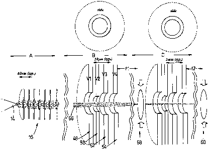
Referring to Figure 4, a complete system is shown comprising two four-element,
cylindrical, einzel lenses, one microscale, labelled, B, and one miniature,
labelled, C.
These lenses axe situated downstream of the electron/ion source labelled, A.
By having
many variables in the geometry they can be made to have very low aberrations.
This is
somewhat analogous to mufti-element optical lenses in cameras and optical
instruments. The final design for these beam elements depends on the
electron/beam
energy, divergence and size as it enters the lens. The parameters which can be
varied
are:
1) The number of elements
2) The thickness of each electrode
3) The spacing between the electrodes
4) The aperture sizes in each electrode
5) The shape of the edges on the lenses as shown in the previous application
6) The voltages applied to each electrode
We have been able, by suitable variations in these parameters to almost
completely
eliminate spherical aberration from our system.
Figure 4 shows the geometry of a four-element lens with electrodes labelled
48, 50, 52
and 54 with voltages V l, V2,, V3, and V4 respectively. The beam and it
direction are
labelled 56. A first analysis position, 58, is a focus distance, fl, from the
end of the
microscale lens. Scanning of the beam is achieved by moving the sample using
piezos
as is usual in scanning tunnelling microscopy. This sample position can be
removed
CA 02492835 2004-12-08
WO 03/107375 PCT/GB03/02560
11
and the beam made to travel through the second miniature lens so as to come to
a focus
at a distance, f2, from the end of the second lens. At this point there is a
piezo driven
sample holder, 60. Although this second miniature lens is shown as having the
same
geometry as the first lens this need not necessarily be the case. Again the
exact
geometry (aperture sizes etc.) will depend on the beam properties as it passes
through
this lens. Typical aperture sizes are around Sp,m for the microscale lens and
Smm for
the miniature lens but these can be varied over a wide range.
A further embodiment of the present invention is shown in Figure 5, wherein a
particle
beam generator is a micro-chip 100 comprising one or more nanocolumns 162
which
produce a narrow (<50 nm) on-axis beam. A nanotip 114 is at the end of a
microstructure which is attached to the vertical cantilever (not shown) and
positioned
centrally and greater than IOnm from the first aperture 13 of the nanocolumn
162.
The nanocolumn 162 can be in one or more parts as shown and defines an axial
beam
of lateral dimensions Less than SOnm. A typical nanocolumnl62 is shown in
figure Sb
and is made of a thin mufti-layer film consisting of alternate metal
(conducting) layers,
118, interspaced with insulating layers 119 through which a circular aperture
13 is
made by lithography or using a focussed ion beam (FIB) 'milling machine'. The
total
length of the nanocolum(s) may be up to 2 ~m and is sufficient to accurately
determine
the (on-axis) direction and phase space emmitance of the beam. The nanotip 114
is
positioned above the aperture as shown and a voltage diferrential is applied
between
the tip 114 and the nanocolumn electrodes 162. The beam defined by the
nanocolumn
has an axis I64 which is concentric with the mufti-element, microscale, einzel
lens.
This lens consists of metal (conducting) electrodes 166 interspaced with
insulators
168. The assembly shown consists of four metal electrodes interspaced with
insulators
and is positioned at distances of only a few microns from the nanocolumn from
which
it is separated by an insulating film with an aperture of the same dimension
as the
microlens. Suitable aperture diameters for this lens are given in the previous
application. Increasing the number of metal conducting electrodes in the stack
can
reduce aberrations in this lens.
CA 02492835 2004-12-08
WO 03/107375 PCT/GB03/02560
12
Figure 6 shows one of the ways of constructing the microscope so that it is
possible for
the microlens to focus the beam at a point less than SO ~.m from the end of
the
instrument. This condition is necessary if the beam is to have a lateral size
less than
lnm and approaching 1 ~,. (This beam spot essentially determines the
resolution of the
instrument.) An application of this embodiment of the present invention is
shown in
near field microscopy in Figure 6b and consists of the 'chip' or body 100
rigidly
attached to a horizontal cantilever arm 170, of a near field microscope, which
can be
positioned using standard techniques of nanopositioning. A vertical cantilever
above
this holds the nanotip II4 and this can be moved vertically and scanned in the
horizontal plane. The sample is mounted on a special retainer 172 which has a
small
surface area for attaching the sample. (This atomic resolution arrangement can
only
accommodate small area samples; for larger areas the focal length of the
microlens is
increased and the resolution degrade to around lnm.) A further vertical
cantilever174
below the microscope body holds the sample retainer and provides a means of
positioning the sample at the correct vertical distance as well as scanning in
the
horizontal plane.
The details of the body or chip 100 are shown in Figure 6a. A series of steps
axe
produced by lithography, or micromachined with laser beams, in one edge of the
chip.
The bottom step is only a few p,ms thick and wider than about 20 ~,m. On this
step
I76 are formed a mufti-layer assembly 178 which is essentially the body of the
particle
beam generator as shown in Figure 6a. The mufti-layer is grown by atomic
deposition
in two stages. First the layers corresponding to the electrostatic lens are
produced and a
hole 113 corresponding to the lens aperture is fabricated in the layers by
lithography
near to the edge of the step corresponding to the letter A in the diagram.
(Many holes
can be produced in one lithographic procedure and each can be a separate
microscope.)
The top layer is covered with a nanometre thick film of gold or carbon and the
successive mufti-layer are then grown (by atomic deposition) corresponding to
the
layer of the nanocolumn. The layers are produce using a horizontal mask which
allows
each separate layer to terminate at a different position along the step. This
provides an
essential method of attaching electrical contacts to the electrodes in the
microscope as
illustrated by the exposed area 180. Finally the nanocolumn hole is drilled
through the
CA 02492835 2004-12-08
WO 03/107375 PCT/GB03/02560
13
top mufti-layer on axis with the electrostatic lens using a focussed ion beam.
(This can
also be made by state of the art e-beam lithography and dry etching
techniques.)
In operation the nanotip 114 is centred on the aperture and the voltages on
the lens
adjusted to focus the beam, with axis 164 onto the sample at focal point 182.
The
thickness of the support step 176 and the focal length are arranged so that
there is a
sufficiently large enough gap for the backscattered electrons to be recorded
with the
channeltron, 184.
Two further adaptations are possible to allow the microscope to be contained
in a
single chip. Firstly the nanotip and a microscopic cantilever can be produced
in the
body of the chip. (This would probably be a horizontal cantilever.) Secondly
the
detector can be fabricated into the base of the chip. For this purpose it is
probably
better to use a semiconducting avalanche type detector for the electrons. It
is even
possible to consider incorporating the mechanisms to scan the sample within
the base
of the chip to make the ultimate SEM on a chip.
In use, typical dimensions and voltages are as mentioned above for the
previous
embodiment of the present invention. A suitable arrangement is for the nanotip
114 to
be positioned using a vertical cantilever arrangement as used in scanning
tunnelling
microscopy (STM). However recent advances in lithography make it possible to
incorporate this cantilever into the microscope itself. The nanocolumn
consists of a
multilayer of conducting (metal or silicon) thin films separated by insulating
layers
through which a circular hole of the required nanoscale size (typically less
than SOnm)
is fabricated. This is made either by lithographic techniques or by drilling
using a
focussed ion beam. A microscale mufti-element einzel lens is positioned below
the
nanocolumn and concentric with it. This can be made as a separate part and can
be
independently positioned with respect to the nanocolumn using standard
micropositioning sytems. In a simpler form the microlens is made into the same
multilayer structure as the nanocolumn and the whole forms the basic element
of the
microscope. Fabrication of the lens can be made by a variety of techniques
including
lithography and laser beam machining.
CA 02492835 2004-12-08
WO 03/107375 PCT/GB03/02560
14
The microscope body is held on a vertical (cantlilever) arm which can be
positioned
both vertically and laterally. The nanoprobe is centred on the nanocolumn
aperture by
a servo- mechanism which uses the current in a quadrant metal thin film which
forms
the first electrode in the nanocolumn. Below the microscope body is a sample
stage on
the end of a vertical cantilever. The electron beam is focussed onto the
sample and can
be moved across the sample by moving the end of the cantilever using standard
nanopositioning techniques as used in STM, for example using piezo-electric
mechanisms. If the backscattered electrons are detected using an electron
detector
(chaneltron) then an image of the atomic structure of the surface can be made.
In the
ultimate design the electron detector can be incorporated into the base of the
microscope chip.
The design for a focussed ion beam system suitable for machining surface
structures
below l Onm can be adapted from the previous description by feeding liquid
gallium to
the nanotip and reversing the polarity of the voltages. In this arrangement
the geometry
is inverted so that the nanotip is positioned below the nanocolumn. (This is
to prevent
liquid gallium from contaminating the microscope.)
A further embodiment of the present invention is shown in Figures 7 and 8,
wherein a
particle beam generator 200 comprises a pair of thin film metallic layers, 212
and 2I3
separated by a semiconductor material 284. Each of the metallic layers
comprises
collimating apertures 286 and 288 (nanocollimators), The beam generator 200
also
comprises an accelerating aperture 220 which extends through the semiconductor
material and shares a longitudinal axis with the collimating apertures 286 and
288. The
diameter of the accelerating aperture 220 is greater than the diameter of each
of the
collimating apertures 286 and 288. Typically, the diameter of the accelerating
aperture
might be around 50 nm and the nanocollimator apertures of about 30 nm.
Particles will
be emitted from the nanotip 214 if a sufficient voltage difference exists
between the tip
and the collimating aperture 286. These particles will be accelerated and
focused into
an almost parallel beam if the voltage difference across the semiconductor is
sufficiently large enough. (The arrow 290 shows the electron beam direction in
both
Figures 7a and 7b). Typically for an 0.5 ~m silicon thin waver, or film, the
voltage
CA 02492835 2004-12-08
WO 03/107375 PCT/GB03/02560
across the semiconductor might be around 300 volts and this will generate a
uniform
field along the hole of 600 MV/m. A longer nanocolumn is possible if it is
made in
two stages as shown in Figure 7b. Here there are two layers separated by a
conducting
film 213. The bottom layer 285 is conducting and can be made from metal or
preferably very low resistivity doped silicon. If the two metal films 213 and
214, are at
earth potential then the whole bottom column 285 is also at earth potential.
The
nanoaperture 286 performs the same function as in the device shown in Figure
7a but
the aperture 288 which can be several microns from the nanotip is able to
reduce
scattering whilst further lowering the (phase space) emittance of the electron
beam.
The hole in this lower column 285 is fabricated at the same time as that of
the upper
accelerating section. Its sole function is to support the nanoaperture 288
concentric
with the hole in the semiconductor. A narrow electron beam, which is limited
in
diameter to the aperture size 288 then passes to the electrostatic focussing
elements of
the microscope as shown in Figure 8.
A complete particle beam generator system for use as a microscope is shown in
Figure
8 with the hole in the nanocolumn 290 and the nanotip 214 being the source of
electrons. The narrow beam of electrons 222 passes from the nanocolumn 286/288
and
through a concentric einzel lens as shown. This lens is a simple three-element
arrangement which is manufactured from conducting and insulating layers, 292
and
294, respectively through which an aperture is manufactured. Multiple element
lenses,
containing five or more electrodes, are also possible to reduce aberrations as
previously mentioned for other embodiments. The inside diameter (aperture of
the
lens) and spacing of the electrodes is chosen to give minimum aberrations and
hence
the smallest beam spot. Typical dimensions for the lens are about 2~m for the
inside
diameter and each layer being about lam thick. Manufacture of the einzel lens
is
simplified if it is made from a single thin waver of three distinct layers.
Using silicon
at different doping concentrations can produce a conducting layer 292 and an
insulating layer 294. For a simple 3 element lens the outer two conducting
electrodes
are at earth potential and the central one is at the correct voltage to give a
focus at the
desired distance from the end of the assembly 296. This whole assembly forms
the
body of the microscope and when this is fabricated at the edge of a stepped
assembly
CA 02492835 2004-12-08
WO 03/107375 PCT/GB03/02560
16
as previously mentioned in another embodiment the beam generator is
essentially a
single chip apart from the nanotip. However this nanotip is at the end of a
cantilever so
that it can be positioned on the centre of the nanocolumn entrance aperture
and can
thus be integrated into the nanochip to make a complete focussed electron
(ion) beam
machine, namely a 'Microscope on a Chip'. Note that the resistive film from
which
the microscope body is made can have many holes in it so that they can all be
accessed
by moving the nanoprobe to any entrance aperture.
In the previous embodiment an accelerating nanocolumn is constructed from a
multilayer structure of alternate metal (conducting) and insulating layers
through
which is a hole of diameter less than 100 nm is fabricated and is the channel
down
which the electrons pass. By applying voltages to the conducting electrodes in
this
assembly it is possible to produce a high electric field along the evacuated
aperture in
the column. This embodiment is a simpler method of producing nanocolumns or
accelerators which have the same effect as the previous assembly. Furthermore
this
new device is simpler to manufacture and can accommodate the inclusion of
restricting
(anti-scatter) collimators at both ends of the column. The method is to
manufacture the
accelerator from a single sheet of high resistivity material through which
holes are
produced using microfabrication techniques. The favoured material, though not
the
only possibility, is single crystal doped silicon as used for the manufacture
of
microchips. The doping will normally be n-type (though p-type is possible) and
the
doping density should be such that the resistivity is in the range froml kS2m-
cm to 100
MS2m-cm but not exclusively. A voltage applied across a thin film of such a
material
will ensure that there is a uniform electric field along any straight hole
through the
resistive material. The hole is made normal to the parallel sides of the thin
wafer or
film, which is the body of the accelerator and can be loosely termed a
nanocolumn, in
line with the previous terminology for a column constructed from a multilayer
of
alternate insulating and conducting thin films. (Nanocolumn is used because
the
because the aperture through the film is in the nanometre size range.) In this
circumstance the electric field is along the (evacuated) hole and it can thus
accelerates
electrons injected into the hole. A nanotip, which can be positioned above a
hole of
typical aperture 50 nm and at a distance of around 30 nm, will field emit
electrons if
CA 02492835 2004-12-08
WO 03/107375 PCT/GB03/02560
17
the voltage on the tip exceeds that of the surface by about 10 volts. Both
surfaces of
the semiconductor are covered with a thin metallic film through which holes
are
manufactured concentric with the hole in the semiconductor. The diameter of
the holes
in the metallic film are smaller than that in the semiconductor so that these
apertures
act as anti-scatter collimators and can also be used to reduce the electron
beam
emittance.
The operation of these nanocolumns in focussed electron and beam devices is as
follows. A negative voltage is applied to the metallic layer nearest to the
nanoprobe
and larger negative voltage is applied to the nanotip. The metallic layer on
the other
semiconductor surface is at earth potential. By choosing these voltages
correctly
electrons emitted from the tip can be focussed and accelerated down the hole
in the
nanocolumn. An almost parallel beam of electrons with diameters less than 50
nm can
be produced.
For the best performance, the diameter of a collimator aperture needs to be
less than
100 nm and the thickness of the silicon larger than 0.5 p,m. If this
arrangement is to be
effective, it is essential that the device contains collimators to both reduce
the
scattering from the walls (of the nanoscale hole) and to reduce the total
emittance of
the beam. The latter can be extremely important since the total emittance of
the beam
is proportional to the final beam spot size. Thus a Iarge decrease in
emittance brought
about by using carefully chosen collimators can lead to a significant
reduction in the
final beam spot size. Two methods are available for producing collimators at
the
nanoscale. In the first method the nanoscale column has a conical hole in it
with the
smaller diameter hole closest to the nanotip electron source. In this way
scattering of
the electron beam from the inside walls of the hole can be largely eliminated.
A
conical shape can be replaced by a form in which the aperture of the hole is
reduced
more abruptly at the position where collimation is required. These collimators
can be
formed at both ends of the tube if needed. In another scheme, a thin metal
covering
layer at either or both ends) of the hole is ion etched to produce a
collimator. This can
be done by dry etching techniques or using a focussed ion beam (FIB) milling
machine.
CA 02492835 2004-12-08
WO 03/107375 PCT/GB03/02560
18
General arrangements are shown in Fig.9, with the electron source being a
nanotip 314
at the entrance to the first nanoscale section of the device with the beam
direction 390
being marked. Figure 9a shows a section of material 301 of micron thickness
through
which is fabricated a SOnm (typical size) circular hole by dry etching
techniques. The
walls of this hole can be made parallel if the etching is carefully
controlled. The whole
microscope column or assembly can be made with accelerating sections and- non-
accelerating sections as described in a previous embodiment. One method of
fabricating these apertures 286 and 288 is as follows. During the production
of the
hole, registration features 398 are produced on the surface to delineate the
aperture
position. The surface is then coated with a nanometer thick gold layer by
vacuum
deposition techniques (atomic deposition from a source) and a 2-3nm (typical)
thick
gold foil, 312 and 313 is placed over the aperture on top of this first layer.
(If this is
done in clean conditions the gold foil will bond to the vacuum deposited gold
layer on
the silicon.) It is then possible to produce apertures, 286 and 288 in this
metal foil by
ion beam drilling or dry etching. (For this to be possible it is important
that the
registration remains visible after the gold layer is applied.) Figure 9b shows
an
alternative way of producing an aperture particularly at the entrance to the
accelerating
section. In this method the hole is tapered into a conical shape as shown.
This tapering
can be produced by carefully controlling the dry etching process. The top
conducting
layer 399 is then made by depositing a metal on the surface using standard
vacuum
deposition methods. A further aperture made by the previous method can be
placed
below this assembly as shown in the central diagram. However it is also
possible to
produce a collimator at this position by placing a second wafer with a tapered
hole in it
below the one shown in the central diagram. This then replaces the aperture
made from
thin film metal (gold). It can be made in a separate thin wafer (of silicon)
which is
positioned so that the holes are concentric or the whole assembly can be
fabricated in
one piece. Thus the system now consists effectively of two wafers with conical
holes
with both wafers vacuum coated on their flat sides with metallic films. It is
also
possible to produce a collimator from the intrinsic material of the wafer not
necessarily
in the form of a taper as is shown in Figure 9c. Collimators can be
manufactured at
CA 02492835 2004-12-08
WO 03/107375 PCT/GB03/02560
19
either or both ends of the assembly or assemblies (wafers). These can be
stacked to
minimise scattering and/or reduce the phase space emittance of the beam.