Note : Les descriptions sont présentées dans la langue officielle dans laquelle elles ont été soumises.
CA 02501110 2005-04-01
WO 2004/032489
PCT/GB2003/004277
SOLID STATE IMAGER
FIELD OF THE INVENTION
The present invention relates to a solid-state imager, in
particular to a charge-coupled device (CCD).
BACKGROUND OF THE INVENTION
In a particular charge coupled device (CCD) imager, signal
charge representative of incident radiation is accumulated
in any array of pixels over an image area. Following an
integration period, signal charge is transferred to an
output register by applying appropriate clocking pulses to
control electrodes. The signal charge is then read out
from the output register and applied to a charge detection
circuit to produce a voltage. The voltage is
representative of the signal charge and hence the
intensity of incident radiation.
A known CCD arrangement is shown schematically in Figure
lA and comprises an image area 10 constituted by an array
of pixels 12 arranged to receive incident radiation from
an image scene. The incident radiation liberates
electrons within the semiconductor structure of the CCD,
the number of electrons liberated being related to the
level of radiation incident on that pixel. After a
defined integration period, the charge accumulated in each
pixel is sequentially moved by application of clocking
pulses to the pixel away from one row to the next as shown
by the arrow A. The rows are successively clocked into a
serial register 14 which itself is clocked in the
direction indicated by arrow B. In this way, charge is
clocked from each pixel, down through the pixel array and
to an output circuit 16 by the serial register 14.
CA 02501110 2011-11-23
2
SUMMARY OF THE INVENTION
We have appreciated the need for introduction of a known
level of charge into a CCD circuit for various purposes, such
as for calibration of the output circuit, for example, or as
a mechanism to avoid the effects of electron capture as a
result of proton or neutron damage. We have further
appreciated, however, that it is difficult to controllably
inject appropriate amounts of charges less than around 10,000
electrons.
Certain exemplary embodiments can provide a charge division
arrangement for a CCD device for producing a divided charge
output from an input charge, comprising an input for
receiving an input charge, an array of elements and an
output, the array of elements being arranged in rows and
columns and having clock connections to allow charge in each
row to be successively clocked from one row of elements to
the next, at least some of the elements being arranged in a
charge division unit having a first element and a second
element in adjacent columns and being communicable at least
temporarily so that charged introduced into the first element
is divided between the first element and the second element,
the charge division unit being arranged to produce divided
charge for production at the output.
Certain exemplary embodiments can provide a CCD imager device
for producing a signal from an image, comprising a plurality
of elements in any array of rows and columns and arranged to
operate in an image mode or a charge division mode, in the
image mode elements in adjacent columns being separated by
CA 02501110 2011-11-23
2a=
barriers, in the charge division mode at least some elements
in adjacent columns being communicable such that charge in
one element is divided between that element and an element in
an adjacent column, whereby charge introduced into one cell
is divided.
The invention may be embodied in two ways. In the first way,
some elements within a CCD imager have isolation regions or
barriers between columns that are selectably removable. This
allows charge introduced into a first row of the imager to be
clocked to successive rows and for charge to be divided
between one column and another as it progresses through the
rows. This allows a defined divided charge to be presented at
an output of the device for input to an output circuit.
Alternatively a permanently enabled splitting structure may
be incorporated in additional columns at the side of the
array which are shielded from incident illumination. In the
second embodiment, a charge division structure as described
is provided in addition to, and at an input of, the CCD
imager. This allows a defined divided charge to be input to
the imager.
In either embodiment, a small charge may be injected into a
final output register. One application of this is to
introduce a "fat zero" which is a small charge level in
CA 02501110 2005-04-01
WO 2004/032489
PCT/GB2003/004277
3
each of the pixels of a register used to fill vacancies
preventing such vacancies affecting an output signal.
BRIEF DESCRIPTION OF THE FIGURES
Embodiments of the invention will now be described by way
of example only and with reference to the figures in
which:
Figure 1A: is a schematic diagram of a known CCD imager
comprising an array of elements in rows and
columns;
Figure 1: is a schematic diagram of a CCD imager
according to a first embodiment;
Figure 2: is a schematic diagram showing how the CCD
imager of Figure 1 may be used; and
Figure 3: is a schematic diagram of a second embodiment
of the invention.
DESCRIPTION OF PREFERRED EMBODIMENTS
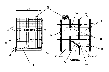
A first embodiment of the invention is shown in Figure 1
with a portion of the imager device shown in expanded form
in the right-hand side of the figure. The imager CCD
device comprises an array of elements 12 comprising an
image area 10 arranged in columns 18 and rows 20. Each
element of the CCD represents a separate pixel in the
final image and comprises clocked CCD cells in a known
manner. The elements are connected to a clock arrangement
(not shown) so that charge accumulated during an image
acquisition integration period in one row can be clocked
from one row to another and finally to an output register
14 to be serially shifted out to an output circuit 16.
As previously discussed, there can be a requirement to
provide a specific amount of charge to the serial register
14 at the end of the register remote from the output
CA 02501110 2005-04-01
WO 2004/032489
PCT/GB2003/004277
4
circuit 16 for purposes such as calibration. Known
techniques involve injecting charge directly into the
serial register. In the present embodiment, however,
charge is injected into a first row of the CCD imager
image area 10 denoted as position 22. The charge injected
at position 22 is sequentially transferred from one row to
another down through the image area 10 to the serial
register14. We have appreciated that use can be made of
the clocking of charge from one row to another to provide
for division of that charge and thereby to allow small
defined elements of charge to be injected from the image
area 10 to the serial register 14. Transfer and division
can occur automatically as part of a normal signal readout
sequence or in a special non-image acquisition mode. The
arrangement for charge division is shown on the right-hand
side of the Figure 1.
Three columns of the array 10 are shown in greater detail
on the right-hand side of Figure 1 showing an array of
elements 12 with column isolation barriers 23 between
them. The configuration of adjacent rows and columns as
shown comprises a charge division unit, which is
configured so that charge introduced at the injection
position 22 can be divided in the sense that a portion of
the charge diverted elsewhere. Such division is
preferably integer division, but could equally be non-
integer division depending upon the relative areas of
charge storage in columns 1 and 2 defined within the
structure. The division unit comprises a first element 24
in a first column adjacent a second element 26 in a second
column. Ordinarily, a column isolation barrier 23 would
be present between the elements 24 and 26. However, when
operating according to the invention, the barrier between
the first element 24 and second element 26 is removed,
shown as position 30, which allows charge to flow from
position 24 to 26. In the event that the barrier is
removed at position 30, the charge at positions 24 and 26
CA 02501110 2005-04-01
WO 2004/032489
PCT/GB2003/004277
will be equal and half the original charge injected at
position 22. This will provide division by two of the
charge amount.
5 As clock pulses are applied to the rows, the charge is
successively clocked down from each column so that
typically half the charge originally injected proceeds
down column 1, whilst the remainder of the charge is
clocked down column 2. A further portion of the isolation
barrier 22 is also selectively removed at position 32 and
an additional barrier at position 34 introduced so that
the excess charge from position 26 is clocked down column
3 from where it may be discarded if not required. The
barriers at positions 30 and 32 may be omitted and re-
established in synergy with the clock pulses clocking
charge from one row to another so that charge clocked down
from column 1 is divided in proportion to the storage
areas of elements (pixels) in the two adjacent columns 1
and 2. Column 2 includes the controllable isolation
region 34, which causes charge to be passed to column 3.
The charge division unit shown in Figure 1 can be repeated
several times down the height of the image area, producing
a charge division each time. The charge division unit is
repeated in corresponding positions so that controllable
(removable or replaceable) isolation barriers such as
shown at position 30 are repeated down the length of the
isolation columns 22 between column 1 and 2 and the
controllable gate type arrangement of the removable
isolation barrier 32 and barrier 34 are repeated between
column 2 and column 3. In this way, charge in column 1 is
repeatedly divided or shared between an element in column
1 and an element in column 2 reducing the charge clocked
down the rows of column 1 each time. The excess charge is
repeatedly passed to column 3 where it can be lost by
transfer to a dump diode 36.
CA 02501110 2005-04-01
WO 2004/032489
PCT/GB2003/004277
6
In the simple case shown of having a removable barrier
between two columns, the simplest case is division of
charge by two. By providing a plurality of such division
units within the image area structure, significant charge
division can be obtained (by repeatedly dividing the
charge by two at each unit). Although the example of a
removable barrier between two columns is shown, it may be
possible to extend the concept to have removable barriers
between more columns to increase the charge division at
each charge division unit. For example, removable
barriers between three columns would allow charge to be
divided by three when charge is clocked to the relevant
position and the isolation columns removed at that
position. Other removable barrier arrangements are
possible and will depend upon the clock speed at which
charges clocked from one row to another. The use of the
selectable barrier at positions 32 and 34 is preferred to
allow excess charge to be removed from column 2. If this
barrier were not present within each division unit, charge
at position 26 would simply be clocked down column 2 such
that it would remain adjacent the charge at position 24
when clocked from one row to another. As a result, charge
would not then flow from column 1 to column 2 - the charge
being equal in both.
In the embodiment in Figure 1, the charge is injected at a
column, three columns from the end of the structure and,
in particular, three columns from the dump diode 36. As a
result, charge is injected to the register at a position
three columns from the right-hand end, being the end
removed from the output circuit 20. The excess charge
from column 3 is passed out through the diode 36.
An alternative embodiment is shown in Figure 2 using the
same arrangement of division units of elements within the
image area, but having a charge injection position 22 near
the left-hand end of the series of columns, namely at a
CA 02501110 2005-04-01
WO 2004/032489
PCT/GB2003/004277
7
column near the output end of the serial register 14
adjacent to the output circuit 16. In this arrangement,
charge is injected into a first column and is successively
divided by removing portions of the charge so that a
divided small amount of charge is presented to the output
circuit 16 without transferring through the serial
register 14. The excess charge is diverted away via diode
36 arranged to take charge from the third column assuming
that the charge division unit is a mirror image of that
shown in Figure 1.
A second embodiment of the invention is shown in Figure 3.
This arrangement also provides a charge division
arrangement or structure, but here is separated from the
elements 12 of a main image area 10 and comprises a
separate structure 38. The separate charge division
structure 38 has a charge injection structure shown as
position 22 as previously described and one or more charge
division units comprising adjacent columns with charges
clocked from the input position 22 along the charge
division structure 38 to an input point 39 of an
additional distribution register 40 for provision to the
image area elements 12. Thus, the rows within the charge
division structure are from top to bottom, in the
schematic diagram of Figure 3, and the columns are from
left to right. Although a single column is shown in
charge structure 38 for ease of representation, this
division structure comprises the three-column arrangement,
as shown in Figure 1. A diode 36 is provided at the third
column of the charge division structure, as previously
described, to remove excess charge.
The distribution register 40 allows charge to be
transferred from the division structure to the main image
array 10. The injection structure at position 22 can be
operated to fill all elements of the distribution register
40, or pulsed to allow a pattern of charge to be loaded
CA 02501110 2005-04-01
WO 2004/032489
PCT/GB2003/004277
8
which would then transfer injected charge into selected
columns of the main array 10. Using the charge
distribution register allows charge to be injected so
that, when transferred down through the rows of the image
area 10, it appears at the end of the serial register
distant from the output circuit in a similar manner to
that shown in Figure 1, or to be injected into the image
area 10 so as to appear at the output circuit 20 without
the requirement to be clocked through the serial register
14. Of course, charge could also be injected at any
position between these two.
In common with the embodiments of either Figure 1, 2 or 3
is that various elements within an array of elements or
cells are arranged so that, as charge is clocked from one
row to another, charge can be divided from one column to
another by use of either permanently removed or
selectively removable isolation regions between columns.
In the case of such arrangement of elements described as
division units within the main image area 10, the regions
between columns which control the division of charge needs
to be selectively removable (or controllable generally in
height) so that the barrier regions are in place when the
array is in a normal image acquisition mode. Otherwise,
there would be a blurring of charge and hence a blurring
of the resultant image. In a charge injection mode in
which charge is to be divided through the array, the
barriers are reduced or removed. In the embodiment of
Figure 3, or where the division structure is incorporated
in additional columns at the side of the image array, the
barrier regions may also be selectively removable, but of
course could also be permanently fixed as present or
absent (or a position between depending upon the division
ratio) as the charge division structure does not also need
to function as an image acquisition area.
CA 02501110 2005-04-01
WO 2004/032489
PCT/GB2003/004277
9
An application of the invention is to inject a small
amount of charge to mitigate neutron or proton damage.
One of the effects of proton (or neutron) irradiation of
silicon is to eject a silicon atom from its position in
the lattice into an interstitial position, leaving a
vacancy. Vacancies are mobile, so wander about until they
can find a more stable state. In a CCD, the region in the
silicon in which charge is transferred (buried channel) is
doped with phosphorous and phosphorous forms a stable
complex with a vacancy. This complex, known as an e-
centre, has an energy state in the middle of the silicon
band gap and so is capable of "trapping" an electron.
While the electron sits at this energy it is also fixed in
space. The effect of having e-centres in the buried
channel of a CCD is seen particularly when transferring
small numbers of electrons, when a significant proportion
can be held by traps, to be released later, after the rest
of the charge signal has moved on.
If all pixels contain a small charge level ("fat zero"),
in addition to the signal, many of the traps will be
continuously filled, allowing the signal charge to be
transferred without loss. Often the "fat zero" needs to
be very small, to minimise excess shot noise, so the
structure shown in Figure 3 would allow the whole device
to be filled from a single low-level injection structure,
giving optimum uniformity.
As previously noted, various alternatives of numbers and
widths of adjacent columns with variable barriers there
between are possible or using the general concept of
charge division by sharing charge between cells or
elements of adjacent columns in an array and such
variations are within the scope of the invention which is
defined in the following claims.