Note : Les descriptions sont présentées dans la langue officielle dans laquelle elles ont été soumises.
CA 02538100 2006-03-07
WO 2005/069430 PCT/US2005/001800
CIRCUIT BOARD ASSEMBLY AND METHOD OF
ATTACHING A CHIP TO A CIRCUIT BOARD
BACKGROUND OF THE DISCLOSURE
[ 1 ] Chips can be attached to a circuit board. For example, antenna arrays
can be assembled
using packaged transmission/receive (T/R) modules. Packaged module assemblies
may be brick
array or coplanar tile arrays. Such packaged assemblies rnay include
fasteners, interconnect
structures and connectors, including, for example, coaxial cable, "fuzz"
buttons, ribbon and/or
wire bonds. Such packages and connecting structures contribute to increased
weight and bulk of
the assembly and increase the amount of board area used. Assembly may also
require numerous
steps which contribute to the time and cost of manufacture_
BRIEF SUMMARY
[2] An antenna array is assembled by a method which includes direct attaching
a flip chip
transmit/receive (T/R) module to an antenna circuit board. A fillet bond is
applied to the circuit
board and the flip chip T/R module around at least a portion of the periphery
of the flip chip T/R
module.
BRIEF DESCRIPTION OF THE DRAWINGS
[3] These and other features and advantages of the invention will readily be
appreciated by
persons skilled in the art from the following detailed description of an
exemplary embodiment
thereof, as illustrated in the accompanying drawings, in which:
[4] FIG. 1 illustrates an exemplary embodiment of a chip attached to a circuit
board.
[5] FIG. 2 illustrates an exemplary embodiment of a chip attached to a circuit
board.
SUBSTITUTE SHEET (RULE 26)
CA 02538100 2006-03-07
WO 2005/069430 PCT/US2005/001800
2
[6] FIG. 3 illustrates an exemplary embodiment of a circuit board with an
array of chip
locations and a chip attached to the circuit board at a chip location.
[7] FIG. 4 illustrates a schematic circuit diagram of an exemplary embodiment
of a T/R chip.
[8] FIG. 5 illustrates a functional block diagram of a controller of a T/R
chip.
[9] FIG. 6 illustrates an exemplary embodiment of a chip attached to, a
circuit with an
underfill.
[10] FIG. 7 illustrates an exemplary embodiment of a chip attached to a
circuit.
[11] FIG. 8 illustrates an exemplary embodiment of a chip attached to a
circuit.
[ 12] FIG. 9 illustrates an exemplary embodiment of a method of assembling an
array of T/R
chips to an antenna panel.
[ 13 ] FIG. 10 illustrates an exploded perspective view of an exemplary
embodiment of a panel
of a flexible antenna circuit board.
DETAILED DESCRIPTION OF THE DISCLOSURE
[ 14] In the following detailed description and in the several figures of the
drawing, like
elements are identified with like reference numerals.
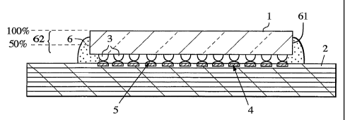
15] Fig. 1 illustrates an exemplary embodiment of a chip 1 connected to a
circuit board 2. In
the exemplary embodiment FIG. 1, the chip 1 is a transmit/receive (T/R) device
chip 1 connected
to a circuit board 2. In the embodiment illustrated in FIG.1, the circuit
board 2 is a mufti-layer
antenna panel circuit assembly. The mufti-layer antenna panel circuit assembly
may be flexible
or rigid. In alternate embodiments, the chip 1 could be a receive chip or any
other chip suitable
for attaching to a circuit board. The circuit board could be any circuit board
suitable for attaching
SUBSTITUTE SHEET (RULE 26)
CA 02538100 2006-03-07
WO 2005/069430 PCT/US2005/001800
3
chips. The circuit board 2 is a medium for distributing power, RF, and digital
signals. The RF
signals may be distributed to an antenna array which could be on the circuit
board or attached to
the circuit board.
[16] The T/R chip is a "flip chip" with connecting portions or "bumps" 3
arranged on the
underside of the chip 1 for connection to corresponding contact pads 4 on the
upper surface of the
circuit board 2. The chip 1 has been connected to the circuit board 2 by a
flip chip or direct chip
attach process. The bumps 3 are connected to the contact pads 4 by a
conductive medium 5. The
connections may comprise microwave, RF, analog, digital and/or DC power
interconnections
between the chip 1 and the circuit board 2. In an exemplary embodiment, the
chip 1 may operate
at microwave or RF frequencies up to at least 11 Ghz. The chip may comprise an
RF T!R chip or
T/R module and may comprise, for example, an Site T/R chip 1.
[ 17] The bumps 3 may comprise solder or solder alloys, for example tin lead
or indium lead
alloys. The contact pads may comprise a conductive material, for example metal
which may be
plated copper. In an alternate embodiment, bumps could be on the circuit board
and contact pads
could be on chips. The bumps 3 and RF traces on the board (not shown) may be
placed over a
dielectric layer, for example bisbenzo-cyclo-butene (BCB). In an exemplary
embodiment, the
dielectric layer can be, for example, one of the CYCLOTENE 4000 Series
electronic resins
(photo BCB), which is available from Dow. BCB may be spun onto the chip in a
liquid state at
the wafer level and cured. The bumps 3 and RF traces on the chip are placed on
top of the
dielectric layer to reduce RF losses and reduce mechanical stress at the
bumped interconnect
when the devices are attached.
[ 1 ~] In the exemplary embodiment of FIG. 1, the conductive medium 5 may
comprise solder
or electrically conductive adhesive (ECA), for example epoxy resin loaded with
silver particles.
In other exemplary embodiments, the conductive medium may comprise
anisotropically
conductive film 51 (ACF) (FIG. 4) and may be connected using pressure or
thermosonic contact
52 (FIG. 5). Any other suitable electrically conductive medium or media for
connecting bumps 3
of a chip 1 to a circuit board 2 could alternatively be used.
SUBSTITUTE SHEET (RULE 26)
CA 02538100 2006-03-07
WO 2005/069430 PCT/US2005/001800
4
[19] In FIG. 1, a fillet bond 6 is placed around at least a portion of the
chip 1, for example
around a portion of the periphery of the chip 1, for bonding the chip 1 to the
circuit board 6. The
fillet bond may comprise non-conductive and/or high viscosity adhesive and/or
may comprise
epoxy, for example silica-loaded epoxy with a viscosity of about 4000
centapoise. The bond 6
may comprise material which has a high flexure modulus, for example about 42
giga-pascals
(Gpa), for holding the chip 1 substantially rigidly to the circuit board 2. In
the exemplary .
embodiment of FIG. 1, the fillet bond 6 is attached at least to a portion of
the sidewall 61 of the
chip 1. 'The bond 6 extends up the sidewall 61 of the chip as far as 50% to
100% of the thickness
of the chip 1. In an alternate embodiment, the bond 6 could extend less than
50% of the
thickness 62 of the chip sidewall 61. In an exemplary embodiment, the fillet
bond 6 extends up
the sidewall 61 to about at least 2/3 of the thickness 62 of the chip 1.
[20] The bond 6 may extend at least partially into the space between the chip
1 and the circuit
board 2. For example, in the exemplary embodiment ofFIG. 1, the bond 6 extends
between the
chip 1 and the circuit board 2 and touches at Ieast the outer edges of the
bumps 3, without
extending beyond the bumps 3. The material used for the fillet bond 6 may be
selected to
provide some control of localized coefficient of thermal expansion (CTE)
mismatch which could
weaken the solder joints. The bond material touches the solder joint and
reduces the solder
mismatch. The fillet bond material may be selected to have desirable strength,
su~ciently high
flexural modulus and to be CTE matched with the chip. 1n some embodiments, the
bond 6 may
extend around the entire edge or perimeter of the chip. A T/R chip 1 with
bumps 3 for making
connections to contact pads 4 of an antenna circuit board 2 can be connected
to the circuit board
2 without a package for housing connection structures. The electrical
connections can be made
through the conductive medium connecting the bumps 3 to the pads 4 and the
chip can be secured
to the circuit board by the conductive medium, a fillet bond and/or underfill,
without any other
connecting or securing structures.
[21 ] FIG. 2 illustrates an exemplary embodiment of a circuit board 2 with a
chip 1 attached. A
fillet bond 6 extends around at least a portion of the chip 1. In the
exemplary embodiment of
SUBSTITUTE SHEET (RULE 26)
CA 02538100 2006-03-07
WO 2005/069430 PCT/US2005/001800
FIG. 2, the fillet bond 6 is not applied to the area on the circuit board 2
wix~;te microwave or RF
signal traces 7 extend out from under the chip 1. The bond 6 may be applied
around the
perimeter of the chip 1 in areas where there are no microwave/RF traces. loot
placing the fillet
bond 6 over 1ZF traces 7 may be particularly suitable for applications with
frequencies above
6GFiz and/or in applications in which degradation in RF signals in RF traces 7
covered by
dielectric material is not desirable. The degradation of signals can be caused
by the difference in
the dielectric constant of the epoxy as compared to the empty space or air
over an uncovered RF
trace.
[22] FIG. 3 illustrates an exemplary embodiment of a circuit board 2 with a
chip 1 attached at
one of a plurality of chip locations 10. A~ fillet bond 6 extends around at
least a portion of the
chip 1 where there are no microwave/RF traces 7. At each chip location 10,
contact pads 4 are
arranged on the circuit board 2 in a pattern corresponding to the pattern of
bumps 3 (FIG. 1 ) on a
surface of the chip 1. The bumps and~the contact pads ~4 are arranged to make
appropriate
microwave, RF, analog, digital and/or DC power interconnections between the
chip 1 and the
circuit board 2. The chip locations 10 are arranged on the board 2 so that the
chips 1 form an
array 100 of chips when attached. An RF signal 71 is input from an array beam
forming network
radar receiver/exciter to RF traces 7 on the circuit board 2. Some of the RF
traces 7 may form a
divider network 72. In the exemplary embodiment of FIG. 2, the RF signal 71 is
divided through
a 1:8 power divider network 72 comprising 7 1:2 power dividers 73a-c. The
array 100 shown in
FIG. 2 may comprise a sub-array of a larger array (not shown). In an exemplary
embodiment, the
array could be as large as hundreds of square meters. 1ZF signal traces 7
connect to RF contact
pads 41. Signal traces 7 from the divider network 72 connect to at least one
of the RF contact
pads 41 at each chip location 10 which corresponds to a bump (not shown) on
the chip 1 for
connecting to a beam forming port (BMF port) 11 of the chip 1. RF traces 7 may
also attach to
RF contact pads 41 corresponding to bumps (not shown) on the chip 1 for
connecting to the low
noise amplifier (LNA) port 12 and a high power amplifier (IIPA) port 13 of the
chip 1 (FIG. 4).
SUBSTITUTE SHEET (RULE 26)
CA 02538100 2006-03-07
WO 2005/069430 PCT/US2005/001800
[23] In an exemplary embodiment, the TR chip 1 of FIG. 3 may operate in the
receive mode at
a frequency range of between 7-11 Ghz, a gain of 9.0 dB, attenuation of S
bits, and phase of 6
bits. In the transmit mode, it may operate in a frequency range of 7-11 Ghz,
with a gain of 17.0
dB, power out of 20.0 dBm (power in=3dBm), an attenuation of 5 bits and phase
of 6 bits. Some
of the contact pads 4 may comprise pads 4 for connecting bumps on the chip 1
corresponding to
ground or to various ASIC functions performed by the controller 31 (FIG. 4).
In the exemplary
embodiment of FIG. 2, for example, a group of interior contact pads 43
correspond to bumps on a
T/R chip for connecting the T/R chip to ground. Other contact pads 4 may also
connect the T/R
chip to ground.
[24] The chip 1 may comprise a "common leg" circuit. In the exemplary
embodiment of FIG.
4, for example, the chip 1 comprises three RF signal ports, namely a BMF port
11, an LNA port
12 and an HPA port 13. The LNA port is switchably connected through transfer
switch 21 to a
forward gain amplifier 14, a first attenuator 15, a phase shifter 16, areverse
gain amplifier 17 and
a second attenuator I 8. The gain amplifiers 14 and 17 may comprise two-stage
hetero-bipolar-
transistor (HBT) gain amplifiers. In the receive mode, a signal 74, for
example from array
radiating element, is input through the LNA port, processed through the gain
amplifier 14,
attenuator 15, phase shifter 16, gain amplifier 17, attenuator 18 through a
switch 22 and switch
23 to the BMF port. In a transmit mode, a signal 71 is input from the beam
steering network to
the BMF port 11, which connects through the switches 23,and 21 (both switched
to positions
which are not shown) to the gain amplifier 14, attenuator 15, phase shifter
16, gain amplifier 17,
attenuator 18, switch 22 (switched to a position which is not shown) to the
driver amplifier 19
and HPA port 13 to the radiating element of a radar array. The drive amplifier
19 may comprise
a single-stage drive amplifier outside of the "common leg" circuit. The chip 1
may also comprise
a digitallanalog controller 31. The controller 31 may perform application
specific integrated
circuit (ASIC) functions. The switches 21, 22, 23 may comprise pin diode, FET
or MEM
switches.
SUBSTITUTE SHEET (RULE 26)
CA 02538100 2006-03-07
WO 2005/069430 PCT/US2005/001800
7
[25] FIG. 5 illustrates an exemplary embodiment of a functional block diagram
of a controller
31 of a T/R chip and exemplary ASIC functions performed by the controller 31.
The ASIC
:functions may comprise digital control logic 32, RAM 33, additional circuitry
34 or digital-to-
analog converter (DAC) 35. The digital control logic 32 may support word
recognition,
reception broadcast and module specific control words, current and next beam
registered data for
RF control, detection of faults to asynchronous communication, whirly gig and
RAM based
mufti-beam registering, driving two different types of phase shi$ers and/or
may provide
negligible power dissipation in a standby mode. The RAM 33 may comprise
storage of volatile
multiple beam data for beam steering. The additional circuitry 34 may
comprise, for example, a
0.3 mW line receiver, a 0.5 mW variable voltage switch control for LNA bias,
base controlled
amplifier bias circuits, pin diode drivers. The DAC may comprise, for example,
voltage settings
for linearly biasing a varactor phase shifter, with, for example, 8 bits of
control to select 255
voltage states. Connections between these functions and corresponding
functions of the circuit
board may be made by flip chip or direct chip attachment of the chip or module
to a circuit board.
In FIG. 1, for example, appropriate bumps 3 on the chip are connected to
corresponding contact
pads 4 on the circuit board 2 by conductive media 5.
[26] In certain exemplary embodiments, the chip 1 may be underfilled. FIG. 6,
for example,
illustrates an exemplary embodiment of a chip 1 attached to a circuit board 2.
Bumps 3 on the
chip 1 may be attached to contact pads 4 on the board 2 by solder or ECA 5. A
fillet bond 6 is
attached to at least a portion of the of the chip 1. Underfill 8 is located
between the chip and the
circuit board. The underfill 8 may comprise an epoxy, for example heavily
filled or loaded (with
silica) or reworkable epoxy. In an exemplary embodiment, the epoxy can be
loaded by as much
as 60%. In alternate embodiments, the underfill may comprise silicon rubbers,
urethanes,
silicones, and/or polymers. In an exemplary embodiment, the circuit board 2 is
first warmed. A
bead of epoxy is dispensed through a needle onto the circuit board 2 around
the perimeter of an
attached chip 1. As the circuit board 2 cools, the expoxy is drawn under the
chip 1, into the
spaces between the chip 1 and the circuit board 2, by capillary action. In an
exemplary
embodiment, the underfill encapsulates the bumps 3.
CA 02538100 2006-03-07
WO 2005/069430 PCT/US2005/001800
8
[27] Underfill 8 may be used, for example, in applications in which the RF
signals do not
experience undesirable degradation from contact with the underfill material.
Epoxy, for example,
may degrade RF signals at frequencies higher thari.about 6GHz. Where signal
degradation is not
an issue, the underfill can be applied without avoiding RF traces. The
underfill 6 may fill up or
nearly fill up the entire space between the chip 1 and the circuit board 2.
[28] In other exemplary embodiments, partial underfill may be used. The
underfill may be
applied such that it does not fill the entire space between the chip and the
circuit board. For
example, in applications in which it is desirable not to cover the RF traces
with unde~ll, the
underfill may be selectively placed in a location and in an amount such that
it does not cover RF
traces when the chip is attached to the circuit board. Partial underfill may
be used in applications
in which it is desirable to avoid covering the RF traces an in applications in
which the RF traces
may be covered. Automated x/y placement equipment can control the needle to
selectively place
the underfill 6 where it will not cover RF traces. Underfill can be used where
the conductive
medium comprises ECA, solder, pressure and/or thermosonic connections.
[29] FIG. 7 illustrates an exemplary embodiment of a chip 1 attached to an
antenna array
circuit board 2 by ACF 51. A fillet bond 6 is provided around at least a
portion of the chip 1.
FIG. 8 illustrates an exemplary embodiment of a chip 1 with solder bumps 3
attached to an
antenna array circuit board 2. The solder bumps 3 are connected to the contact
pads 4 by either a
pressure or a thermosonic contact 52. In a thermosonic contact, the bumps 3 of
the chip 1 are
held against the contact pads 4 on the circuit board 2 and subjected to
ultrasonic vibrations which
can cause the bumps to form a bond with the contact pads 4. A fillet bond 6 is
provided around
at least a portion of the chip 1.
[30] In various exemplary embodiments, the conductive medium may be applied by
a variety
of methods. FIG. 9, for example, illustrates a block flow diagram of an
exemplary method of
assembling an array of T/R chips on an antenna circuit board. The method
illustrated in FIG. 9
includes applying a conductive medium 201, placing the chip on a board 202 and
bonding the
chip to the board 203. Applying the conductive medium may comprise at least
one of applying
SUBSTITUTE SHEET (RULE 26)
CA 02538100 2006-03-07
WO 2005/069430 PCT/US2005/001800
9
the conductive medium to contact pads of a circuit board or applying a
conductive medium to a
chip, for example to the bumps of a T/R chip. Applying a conductive medium may
comprise, for
example, screen printing 201 a a medium, for example ECA, directly onto a
flexible circuit board
or dipping 201b the bumps of a chip into a paste. Dipping 201b the bumps of a
chip into paste
may be performed using a pick and place machine. Any other suitable means for
applying the
conductive medium may be used without departing from the scope of this
invention.
[31 ] The method illustrated in FIG. 9 also comprises placing the chip 202 on
the circuit board.
The chips may be placed onto a circuit board automatically by a pick and place
machine. In an
exemplary embodiment, the pick and place machine may be used to dip 201b the
bumps of a chip
into paste and then to place the chip 202 onto the circuit board. Directly
attaching T/R modules
to a flexible circuit array may provide a low profile, lower weight
alternative to other assembly
methods. It may also provide shorter interconnect paths and permit automated
assembly of active
arrays using commercially available pick and place equipment. Pick and place
equipment is
available, for example, from Universal Instruments Corp. of Binghamton, New
York. In an
exemplary embodiment, placing the chip 202 may comprise aligning the chip 202a
with the
circuit board using, for example, a vision system and fiducials located at
least on the chip and the
circuit board.
[32] After placing the chip 202 in the desired location, the conductive medium
may be bonded
203 to the board. Bonding to the board may comprise curing 203a, for example
ECA, or
reflowing solder 203b in an oven or belt furnace, depending on the conductive
medium being
used. In alternative, exemplary embodiments, bonding the chip to the board may
comprise
applying pressure 203c: Applying pressure 203 may be used during a cure 203a,
for example,
where the conductive medium comprises an anisotropcially conductive adhesive
or
pressure/thermosonic contact. In an exemplary embodiment, bonding the chip to
the board may
also comprise application of a fillet bond 204 and or underfill 205.
(33] The assemblies and assembly methods described herein may be applied to
large-scale
flexible antenna circuit panels. Large-scale flexible antenna circuits may be
fabricated using reel
SUBSTITUTE SHEET (RULE 26)
CA 02538100 2006-03-07
WO 2005/069430 PCT/US2005/001800
to reel flexible manufacturing processes, which may allow the manufacture of
large flexible
panels with sizes of several square feet. Antenna arrays may be as large as 10
squar,° meters or
more. Individual flexible panels may have a width of up to about a meter wide.
The maximum
width of the individual panels forming an assembly may be limited by the size
of the pick and
place machines available for use in placing chips on circuit boards.
(34] FIG. 10 illustrates an exploded perspective view of an exemplary
embodiment of a panel
of a flexible antenna circuit board 2. The circuit board 2 comprises a circuit
film layer 201 with
T/R chips 1 attached to the bottom side, a signal/power circuit film layer
202, a bottom-side
ground plane layer 203, an air strip line secondary feed layer 204, a
cicrulator mounting board
205 and a strip line circuit board 206 with disk aperture radiating elements
207 mounted on the
top-side. In this exemplary embodiment, each layer is separated from adjoining
layers by a layer
of adhesive 208. The secondary feed layer comprises z-axis gasket layers 209,
top and bottom,
with kapton circuit film 210. The circulator mounting board 205 comprises
pockets 211 which
enclose three-port circulators 212.
[3 5] ' The assemblies and assembly methods described herein may provide for
higher density
antenna arrays with lighter weight interconnect structures, when compared to
other assemblies or
assembly methods. Higher density and lighter weight assemblies may be used,
for example, in
space based radar antenna arid "smart skin" avionics applications, in which
flexible circuit boards
are applied in a conformal manner over the body or skin of the platform, or
any other
applications. The assemblies and assembly methods described herein may provide
interconnect
structures for simultaneous microwave, digital and DC power interconnections,
as well as
structural attachments, between T/R modules andlor flexible circuitpanel array
antennas, without
the bulk or weight associated with other assemblies or assembly methods.
[36] It is understood that the above-described embodiments are merely
illustrative of the
possible specific embodiments which may represent principles of the present
invention. Other
arrangements may readily be devised in accordance with these principles by
those skilled in the
art without departing from the scope and spirit of the invention.
SUBSTITUTE SHEET (RULE 26)