Note : Les descriptions sont présentées dans la langue officielle dans laquelle elles ont été soumises.
CA 02540146 2010-07-16
WO 2005/031980 PCT/IB2003/004846
Accumulator for Adaptive Sigma-Delta Modulation
Technical Field
The invention generally relates to signal processing, and more particularly, -
to
analog to digital conversion using sigma-delta modulation.
Background Art
Sigma-delta (E-A) modulation is a widely used and thoroughly investigated
technique for converting an analog signal into a high-frequency digital
sequence. See, for
example, "Oversampling Delta-Sigma Data Converters," eds. J. C. Candy and G.
C.
Temes, IEEE Press, 1992, (hereinafter Candy) and "Delta-Sigma Data
Converters," eds.
S. R. Northworthy, K. Schreier, G. C. Temes, IEEE Press, 1997.
In E-A modulation, a low-resolution quantizer is incorporated within a
feedback
loop configuration in. which the sampling frequency is much higher than the
Nyquist
frequency of the input signal (i.e., much higher than twice the maximum input
frequency). In addition, the noise energy introduced in the quantizer is
shaped towards
higher frequencies according to a so called "noise-transfer-function" NTF(z),
and the
signal passes the modulator more or less unchanged according to a so called
"signal-
2o transfer-function" STF(z).
Fig. 1(a) depicts a simple first order E-11 modulator for a discrete time
system
having a subtraction stage 101, an accumulator 102 (including an integrator
adder 103
and a delay line 104), a one-bit quantizer 105, and a 1-bit digital-to-analog
converter
(DAC) 106. In normal operation, an input signal x(n) within the range [-a, +a]
is
converted to the binary output sequence yo(n) E 1. Quantizer 105 produces a
+1 for a
positive input and a -1 for a negative input. The output from quantizer 105 is
fed back
through DAC 106 and subtracted from input signal x(n) by subtraction stage
101. Thus,
the output of subtraction stage 101 represents the difference between input
signal x(n)
and the quantized output signal yo(n). As can be seen from Fig. 1(a), the
output of
accumulator 102 represents the sum of its previous input and its previous
output. T'hus,
depending on whether the output of the accumulator 102 is positive or
negative, the one-
1
SUBSTITUTE SHEET (RULE 26)
CA 02540146 2010-07-16
WO 2005/031980 PCT/IB2003/004846
bit quantizer 105 outputs a +1 or a -I as appropriate. Herein, and in the
appended claims,
analog (physical) and digital representations ofsignals are distinguished from
each other
by labeling digital one or multi-bit signals with the subscript "0".
In Fig. 1(b), a linear model of Fig. 1(a) is shown, and similarly includes a
subtraction stage 107, and an accumulator 111 (including an integrator adder
112 and a
delay line 113). Quantizer 105 is replaced by an adder 108 and a noise source
109. To
convert signal y(n) to yo(n), a comparator 110 for detection of the sign of
y(n) is included.
The basic relationship between the z-transforms of system input x(n),
quantizer noise
ya(n), and the two-level output sequence y(n) is:
Y(Z) = Z"X(z) + (1- z')ra(Z) (1)
The signal transfer function and noise-transfer function can be identified as
STF(z) = Z-1
and NTF(z) = (1-z'), respectively.
Quality of digital repfesentation can be described, by the signal-to-noise
ratio
SNR =10log,o N , where S is the signal power and N is the noise power within a
given
bandwidth B. Regarding equation (1), the noise power N depends on both the
noise
transfer function NTF(z) and the overall amount of noise ra(z) added in the
quantization
stage. To improve the SNR, two approaches can be pursued:
(a) for a given overall noise power Fa(z), i.e., for given quantizer levels
a,
modify the NTF(z) to remove more noise power from the base band by improved
noise
shaping, and
(b) for a given NTF(z), try to reduce the overall noise power introduced to
the
system.
Approach (a) can be achieved, for example, by increasing the order of the
sigma-
delta modulator, as described by Candy. For higher order modulators, the noise
transfer
function becomes NTF(z) = (I-z')k, which means an enhanced noise-shaping
effect. For
examples of approach (b) see Zierhofer C.M., "Adaptive sigma-delta modulation
with
one-bit quantization," IEEE trans. CAS H, vol. 47, No. 5, May 2000
(hereinafter
Zierhofer), and U.S. Patent Application for Adaptive Sigma-delta Modulation
with One-
bit Quantization, issued as U.S. Patent 6,535,153, where a sigma-
delta modulator is employed within a feedback loop configuration. It is shown
that the
2
CA 02540146 2006-03-24
WO 2005/031980 PCT/IB2003/004846
input signal of this modulator applies within a reduced range, and thus the
two levels of
the quantizer can be reduced. As a consequence, less noise power is introduced
to the
system, and the SNR is improved.
Summary of the Invention
In connection with developing an adaptive sigma-delta (E-A) modulator, a new
accumulator stage for use in a non-adaptive or adaptive sigma-delta (E-A)
modulator was
invented. In accordance with one embodiment of the invention, a system and
method for
an adaptive sigma-delta (E-A) includes an input stage that produces a
difference signal
representing the difference between an analog input signal x(n) and an analog
feedback
signal z(n). The amplitude of the analog input signal x(n) is within a first
range [-a, +a].
An accumulator stage produces an accumulated signal that is a function of an
accumulation of the difference signal, the accumulator stage transforming the
accumulation of the difference signal so as to increase average magnitude
while ensuring
instantaneous magnitude does not exceed a predetermined value. A quantization
stage
produces a quantized digital signal yo(n) representing the accumulated signal.
Based on
the quantized digital signal yo(n), an adaptation stage produces a digital
output signal
zo(n), which is converted to the analog feedback signal z(n) by a digital-to-
analog
converter.
In related embodiments of the invention, the adaptation stage tends to keep
the
instantaneous magnitude of the analog feedback signal z(n) within the first
range [-a, +a]
and greater than the analog input signal's x(n) instantaneous magnitude. The
accumulator
stage may include an accumulation capacitor, the charge across the capacitor
representing
an accumulation of the difference signal. The accumulated signal may be based,
at least
in part, on the voltage across the accumulation capacitor. The capacitance
across the
accumulation capacitor may be variably controlled such that average magnitude
of
voltage across the accumulation capacitor is increased while ensuring
instantaneous
magnitude of voltage across the accumulation capacitor does not exceed the
predetermined value. The accumulation capacitor may be coupled between an
input and
an output of an operational amplifier.
In further related embodiments of the invention, the adaptation stage may
include
a multiplier stage that multiplies the quantized digital signal yo(n) by a
step size co(n), and
the capacitance across the accumulation capacitor is variably controlled
based, at least in
3
CA 02540146 2006-03-24
WO 2005/031980 PCT/IB2003/004846
part, on the step size co(n). The accumulation capacitor may include an array
of
capacitors, each capacitor in the array capable of being switched so as to
vary the
capacitance across the accumulation capacitor.
In still further related embodiments of the invention, the digital-to-analog
converter may include an array of weighted capacitors, the array of weighted
capacitors
capable of acquiring a charge QDAC(n) negatively proportional to the digital
output signal
zo(n). The input sampling stage may include an input sampling capacitor, the
input
sampling capacitor capable of acquiring a charge Qin(n) proportional to the
analog input
signal x(n).
In yet other related embodiments of the invention, the quantized digital
signal
yo(n) produced may include a two-level digital output sequence. The two-level
digital
output may include values of +1 and -1. Producing the digital output signal
zo(n) may
include multiplying the quantized digital signal yo(n) by a step size co(n).
The step size
co(n) may be based on a set Y of code words, where Y={yo(n), yo(n-1), yo(n-
2)...yo(n-
nX) }, nX being a predetermined integer. Determining the step size co(n) may
include
increasing the step size co(n) if a majority of the code words are equal, or
decreasing the
step size co(n) if the code words alternate. The step size co(n) may be non-
linear.
Multiplying the quantized digital signal yo(n) by a step size co(n) may
include using a
look-up-table RAM.
In another embodiment of the invention, a system and method for an adaptive
sigma delta modulator includes an input stage that produces a difference
signal
representing the difference between an analog input signal x(n) and an analog
feedback
signal z(n). The amplitude of the analog input signal x(n) is within a first
range [-a, +a].
An accumulator stage produces an accumulated signal that is a function of an
accumulation of the difference signal. The accumulator stage includes an
accumulation
capacitor having a capacitance that is capable of being variable controlled.
The charge of
the accumulation capacitor represents the accumulation of the difference
signal. A
quantization stage produces a quantized digital signal yo(n) representing the
accumulated
signal. Based on the quantized digital signal yo(n) an adaptation stage
produces a digital
output signal zo(n). A digital-to-analog converter stage converts the digital
output signal
zo(n) to the analog feedback signal z(n).
In related embodiments of the invention, the accumulation capacitor may be
variably controlled so as to increase the average magnitude of the voltage
across the
accumulation capacitor while ensuring an instantaneous magnitude of the
voltage across
4
CA 02540146 2006-03-24
WO 2005/031980 PCT/IB2003/004846
the accumulation capacitor does not exceed a predetermined value. The
accumulation
capacitor may include an array of capacitors, each capacitor in the array
capable of being
switched so as to vary the capacitance across the accumulation capacitor. The
adaptation
stage may include a multiplier stage that multiplies the quantized digital
signal yo(n) by a
step size co(n), and wherein the capacitance across the accumulation capacitor
is variably
controlled based, at least in part, on the step size co(n). The adaptation
stage may tend to
keep the instantaneous magnitude of the analog feedback signal z(n) within the
first range
[-a, +a] and greater than the analog input signal's x(n) instantaneous
magnitude.
In accordance with another embodiment of the invention, a sigma delta
modulator
includes an input stage that produces a difference signal representing the
difference
between an analog input signal x(n) and an analog feedback signal z(n). An
accumulator
stage produces an accumulated signal that is a function of an accumulation of
the
difference signal. In particular, the accumulator stage transforms the
accumulation of the
difference signal so as to increase average magnitude while ensuring
instantaneous
magnitude does not exceed a predetermined value. A quantization stage produces
a
quantized digital signal yo(n) representing the accumulated signal. A digital-
to-analog
converter stage converts the digital signal yo(n) to the analog feedback
signal z(n).
Brief Description of the Drawings
The present invention will be more readily understood by reference to the
following
detailed description taken with the accompanying drawings, in which:
Fig. 1(a) is a block diagram of a prior art first order E-A modulator for a
discrete
time system;
Fig. 1(b) is a block diagram of a prior art first order E-0 modulator for a
linear
model, where the quantizer is replaced by an adder and a noise source;
Fig. 2 is a block diagram of an adaptive sigma-delta (E-A) modulator with one
bit
quantization that improves the signal-to-noise (SNR) of a E-0 modulator in
accordance
with one embodiment of the invention;
Fig. 3(a) shows representative waveforms for an adaptive sigma-delta (E-0)
modulator in accordance with one embodiment of the invention;
Fig. 3(b) shows representative waveforms for an adaptive sigma-delta (E-0)
modulator in accordance with one embodiment of the invention;
5
CA 02540146 2006-03-24
WO 2005/031980 PCT/IB2003/004846
Fig. 4 shows SNR-simulation results representative of various types of analog-
to-
digital converters;
Fig. 5 shows SNR-simulation results representative for adaptive sigma-delta (E-
A)
modulators with ideal and non-ideal digital-to-analog converters in accordance
with one
embodiment of the invention;
Fig. 6 is a block diagram of an adaptive sigma-delta (E-A) modulator with one
bit
quantization that includes a high pass filter stage in accordance with one
embodiment of
the invention;
Fig. 7 is a block diagram of an adaptive sigma-delta (E-0) modulator with one
bit
quantization having a high pass filter stage that includes a numeric multibit
sigma-delta
modulator in accordance with one embodiment of the invention;
Fig. 8 shows representative waveforms for the system depicted in Fig. 7;
Fig. 9 shows SNR-simulation results pertaining to the signal-to-noise ratio
for the
system depicted in Fig. 7;
Fig. 10 shows a block diagram of an analog stage of an adaptive sigma-delta
modulator, in accordance with one embodiment of the invention; and
Fig. 11 shows a variable accumulation capacitor, in accordance with one
embodiment of the invention.
Detailed Description of Specific Embodiments
A method and system for an adaptive sigma-delta (E-A) modulator with one bit
quantization that improves the signal-to-noise (SNR) of a E-A modulator is
presented. A
block diagram of the system in accordance with one embodiment of the invention
is
shown in Fig. 2. The output yo(n) and two level feedback signal y(n) E a of a
standard
E-0 modulator of 15` order is replaced by a multilevel output signal zo(n) and
feedback
signal z(n), respectively. The instantaneous magnitude of the multilevel
feedback signal
z(n) is kept within the range [-a < z(n) < a] and greater than the
instantaneous magnitude
of the input signal x(n) by an adaptation stage 205. Compared to the non-
adaptive
modulator, the noise source 107 in Fig. 1(b) is thus reduced, and the SNR is
considerably
enhanced. The adaptation algorithm of the adaptive E-A presented can be fully
exploited,
if the input x(n) is a zero-mean signal, or if the dc-component of x(n) is at
least close to
zero. If x(n) contains a considerable dc-component, the input dynamic range is
reduced.
Accordingly, an implementation of a high-pass filter stage is also presented.
6
CA 02540146 2006-03-24
WO 2005/031980 PCT/IB2003/004846
Fig. 2 can be separated into an analog and a digital section. An analog input
x(n)
having range [-a, +a], is inputted into a subtraction stage 208. The analog
output of the
subtraction stage is then inputted into an accumulator 209 (including an
integrator adder
210 and a delay line 211) and then quantized 202. The digital output of the
quantizer
202, which may be, but is not limited to, yo(n) E 1, is multiplied 207 by a
step size
sequence co(n) to create output signal zo(n). Output signal zo(n) is passed
through a
digital-to-analog converter (DAC) 204 to create the analog feedback signal
z(n).
Step size sequence co(n) is generated in an adaptation stage 205. The step
size
co(n) at a particular instant is controlled by a set of code words
[yo(n), yo(n-1), yo(n-2), ... ], which represent the instantaneous value of
yo(n), and a
particular (finite) number of previous code words yo(n-1), yo(n-2) ... The
primary
intention of adaptation stage 205 is to keep the instantaneous magnitude of
z(n) greater
than the instantaneous magnitude of input signal x(n),
jz(n)l > jx(n)j. (2)
The way the adaptation stage works is intuitively clear. Step size co(n) needs
to
be increased, if the set [yo(n), yo(n-1), yo(n-2), ...] contains many equal
code words. In
this case, jx(n)l tends to exceed jz(n)j, which violates condition (2). On the
other hand,
co(n) needs to be decreased, if the set [yo(n), yo(n-1), yo(n-2), ... ] shows
an alternating
pattern of code words.
Using, for example, a 9-bit DAC 204 for the system shown in Fig. 2, the input
range [-a, +a] is subdivided into 511 equally spaced discrete signal levels.
Thus, the
digital signals zo(n) and co(n) are composed of 9 bits, and 8 bits,
respectively. In
accordance with one embodiment of the invention, an adaptation algorithm for a
system
of 1st order, with constant a chosen to be a = 16 , is provided in Tab. 1.
As shown in Tab. 1, the step size is increased by approximately a factor a3,
if
five consecutive code words are equal, and decreased by about a factor
(X-', if four consecutive code words have alternating signs. Since step sizes
co(n) have a
30 limited resolution of 8-bits, the products a3co (n -1) and a-'co (n -1)
cannot be
implemented exactly, but have to be rounded to the next integer. For small
step sizes, the
deviations due to rounding are considerable, but this type of imperfection is
not essential
7
CA 02540146 2006-03-24
WO 2005/031980 PCT/IB2003/004846
Table 1
Code Step Size Multiplier
yo(n) = yo(n-1) = yo(n-2) = yo(n-3) = yo(n-4) co(n) = round((x 3co(n-1))
Yo(n) = -yo(n-1) = yo(n-2) = -yo(n-3) co(n) = round(c(1co(n-1))
F Other combinations co(n) = co(n-1)
for the system performance. While a multiplier can be used to calculate co(n),
in various
embodiments of the invention, a look-up-table RAM 206 is utilized instead,
where all
possible step sizes co(n) are stored as 8-bit integers, for example. The
minimum and
maximum step sizes are then co,,,,;,, = 1 and co,. = 255, respectively. The
computation of
product a3co (n) may be achieved by simply increasing the instantaneous RAM-
address
index by 3. Similarly, for product a-lco (n) , the instantaneous address index
is
decreased by 1.
Sample waveforms for an adaptive E-A modulator implementing the adaptation
algorithm described in Tab. 1 are shown in Figs. 3(a ) and 3(b). The first
trace 301 in
Fig. 3(a) depicts an example of an input signal x(n). The second trace 302 in
Fig. 3(a)
shows the full wave rectified version jx(n)l together with the magnitude
jz(n)l of the
DAC-output signal. Condition (2) is fulfilled for almost all samples, but a
close
examination shows that there is a violation at instant n = 1643. This remains
singular,
however, and has negligible impact on the overall performance of the system.
The third
trace 303 in Fig. 3(a) illustrates the full DAC-output signal z(n). In Fig.
3(b), the system
behavior is shown, if signal x(n) is attenuated by 40dB, i.e. for x(n)/100.
Traces 304, 305,
and 306 represent an input signal x(n), the full wave rectified version jx(n)l
together with
the magnitude jz(n)l of the DAC-output signal, and the full DAC-output signal
z(n),
respectively. As expected, the quantization of signals jz(n)l and z(n) appears
more
pronounced, and the digital sequence co(n) varies between 1 and 3.
The examples Figs. 3(a) and 3(b) also demonstrate that the step-size
adaptation
algorithm works instantaneously, that is, step size multiplier c(n) tracks the
individual
maxima and minima of input x(n). Signal c(n) can directly be used to estimate
the
instantaneous power of the input signal, which is advantageous, for example,
in signal
processing applications for automatic gain control (AGC) for speech signals.
Adaptive
8
CA 02540146 2010-07-16
WO 2005/031980 PCT/IB2003/004846
E-A modulation schemes typically use comparatively slow adaptation algorithms,
where
time constants in the range of tens of milliseconds are involved (usually
referred to as
"syllabic compression"). An example is Chakravarthy, C. V., "An amplitude-
controlled
adaptive delta sigma modulator," Radio & Electronic Engineer (London), vol.
49, pp. 49-
54, January 1979. Systems like this cause
gross errors in case of sudden increase of the amplitudes of the input signals
and are not
practical in signal processing applications, where a permanent accurate
representation of
the input signal is of importance. Additionally, the use of non-linear step
sizes makes the
adaptive algorithm more responsive to changes in input amplitudes compared to
prior art
adaptive algorithms with a constant step size, such as described in Jaggi,
M.P.,
"Instantaneously Adaptive Delta Sigma Modulator" Can. Elect. Eng. 1, Vol. 11
No. 1,
1986. This is important, for example, in
keeping the instantaneous magnitude of the first analog feedback signal
greater than the
input signal's instantaneous magnitude.
In Fig. 4, the SNR of various types of analog-to-digital converters are shown
as a
function of the input signal's power. The input x(n), within the range [-1 <
x(n) < 1] (i.e.,
a = 1), is a periodic zero-mean noise sequence composed of 10000 samples, and
the
bandwidth is B = 10kHz. Within this bandwidth, amplitudes and phases of the
spectral
lines are randomized. Different values of signal power are obtained by
proportional
amplification of this signal. The input power is referenced to the power level
of a dc-
signal with amplitude a = 1. At the maximum input power level shown in Fig. 4
(i.e., at
-9.45dB), the maximum signal amplitude reaches 0.99, which is just below the
limit
of the reference level a = 1. The sampling rate for all systems is T = 1MHz,
and the
SNRs are computed within B = 10kHz.
Curve 401 depicts the SNR of an ideal adaptive sigma-delta modulator in
accordance with one embodiment of the invention, where the adaptation
algorithm of
Tab.l and a 9-bit DAC is used (a = 1). Reducing the input power from the
maximum
level to lower levels, the SNR tends to remain constant. For input levels
smaller than
about -50dB, the SNR is decreasing. Curve 402 is the SNR of an ideal standard
sigma-
delta modulator of 151 order with ya(n) E 1. The maximum SNR is obtained at
the
maximum input power level, and a decrease of input power results in a decrease
of the
SNR. Comparing curves 401 and 402 clearly demonstrates the benefit of the
adaptive
sigma-delta modulator. Curve 402 is very similar to the segment of curve 401
having
9
CA 02540146 2006-03-24
WO 2005/031980 PCT/IB2003/004846
input levels smaller than about -50dB, shifted to the right by about 48dB.
This shift
reflects the additional 8 bits of signal z(n) as compared to ya(n). For input
levels smaller
than about -50dB, the adaptive sigma-delta modulator operates in a manner
similar to a
standard sigma-delta modulator, since the feedback-signal z(n) is a two-level
signal,
z(n) E 1/256. Note that for high input levels, the SNR of the adaptive
modulator is not
substantially higher than for the standard modulator. However, the input
dynamic range
has been expanded by approximately 48dB. Curve 403 depicts the SNR of a sigma-
delta-
modulator of 2nd order. Obviously, at lower input levels, the 2nd order system
is
outperformed by the adaptive modulator. Curves 404 and 405 depict the SNR's of
Pulse
Code Modulation (PCM) systems with 13 and 14 bit resolutions, respectively.
Whereas
the 14-bit PCM system is superior to the adaptive sigma-delta modulator for
all input
levels, the 13-bit PCM system is inferior at least at low-level input signals.
In accordance with one embodiment of the invention, the adaptive sigma-delta
modulator includes a multi-bit DAC 204 in the feedback loop, as shown in Fig.
2, since
the feedback signal z(n) is a multi-level signal. In preferred embodiments of
the
invention, the specifications of this DAC 204 is chosen to have minimal
effects on the
SNR of the adaptive sigma-delta modulator. The non-ideal DAC can be regarded
as an
ideal converter plus a noise source, with the transfer function of this
additional noise
source being -NTF(z) = -z 1. Thus, this noise (multiplied by -1) is directly
added to the
input signal and enhances the noise energy in the base band. For the DAC 204,
the
following assumptions can be made:
(1) The distribution of DAC-errors is symmetric around zero.
(2) Each discrete DAC-levels is implemented by means of superposition of
binary
weights.
(3) Each binary weight itself is composed of elementary unit components. This
implies, e.g., that for a particular binary weight which is composed of K unit
components,
the nominal value is increasing proportional to K, whereas the error is
increasing
proportional only to .
For example, for a 9-bit DAC, the pattern co(n) = [1 0 0 10 10 1] contains the
binary weights 128, 16, 4, and 1, and hence the nominal magnitude of the
resulting DAC-149 level is 255 a. However, the single weights can only be
realized as 128 1 A 128
CA 02540146 2006-03-24
WO 2005/031980 PCT/IB2003/004846
16 1 J, 4 1 l, and (1 A), which results in a deviation from the nominal
16 ( ~vF4l
value.
Fig. 5 shows the SNRs of an adaptive sigma-delta modulator with an ideal 9-bit
DAC (A = 0) 501, and non-ideal DACs for A = 1% 502, A = 3% 503, and A = 5%
504,
where A denotes the maximum deviation of the implemented level number K = 1
from
the nominal value. In all cases, the contribution of the dc-offset error is
omitted, and the
input signal is the same as for Fig. 4 (N = 10000). Fig. 5 shows that the SNR
reduction
will be within acceptable limits with parameters A better than about A = 1 %.
The adaptive sigma-delta modulator shown in Fig. 2 yields its optimum
performance if the input x(n) is a zero-mean signal, or if the dc-component of
x(n) is at
least close to zero. However, if x(n) contains a considerable dc-component,
the input
dynamic range is reduced. Consider, for example, an input signal with a dc-
component
and comparatively very small ac-component. The step size reduction will be
governed by
the dc-component and not the ac-component, and thus it remains too large.
Dc-components can be introduced from either the input signal directly, or by
offset-errors
due to non-ideal components of the modulator itself. In practical
implementations, offset
errors in the DAC might occur. In any case, a high-pass filter removes most
problems
involved with dc- or very low frequency components.
In accordance with one embodiment of the invention, an implementation of a
high-pass filter is implemented as shown in Fig. 6. Here, the adaptive sigma-
delta
modulator 203 of Fig. 2 is embedded in a feedback loop system, which
represents a
typical digital high-pass filter. The digital output zo(n) of the modulator is
first
accumulated 601, resulting in signal azo(n), and then multiplied 602 by a
factor 0,
resulting in signal wo(n). Digital-to-analog conversion of wo(n) by means of a
second
DAC 603 results in signal w(n), which is subtracted 604 from the input x(n).
The overall
signal-transfer-function STFHP(z) of such a system is given by
STF,,p (z) = STF(z)HP(z), (3)
with the standard E-A signal-transfer-function, i.e., STF(z) = z-', and the
high-pass
transfer-function HP(z) = 1- z I . There is a zero at z = 1 corresponding to a
1-(1-0)z-
11
CA 02540146 2006-03-24
WO 2005/031980 PCT/IB2003/004846
frequency f = 0, and a pole at z = 1-0. Using, for example, a sigma-delta rate
of 1MHz
and 0 = 1 results in a 3-dB cut off frequency of about 150Hz.
1024
The system shown in Fig. 6 is not well suited for practical implementation,
since a
19-bit DAC is involved. Therefore, in accordance with various embodiments of
the
invention, means to circumvent such a high precision DAC are implemented. In
accordance with one embodiment of the invention, inserting a numeric version
of a
multibit sigma-delta modulator 701 into the system results, for example, in
the system as
shown in Fig. 7. Assuming 0 = 1
g 1024 'signal azo(n) comprises 19 bits. Following the
general rules of sigma-delta modulation, this signal is converted to output
signal
1024wdo(n), which represents the input signal azo(n), delayed by one clock
period. In the
present application, signal wo(n) = wdo(n+l) is used as a high-pass filter
feedback signal,
which represents the non-delayed input azo(n), multiplied by 1/1024. In the
present
embodiment, two identical 9-bit numeric quantizers 702 and 703 with a transfer
characteristics of mid-tread-type are employed. Possible output numbers are -
255, -254,
.., -2, -1, 0, 1, 2,... 254, 255. Note that using the numeric multibit sigma-
delta modulator
provides a very efficient method to implement the constant-factor
multiplication 1/1024.
azo(n)
Signal wo(n) is the sigma-delta version of signal 1024 . Thus, the number of
bits
has been reduced from 19 in signal azo(n) to 9 in signal wo(n). However,
following the
principles of multibit sigma-delta modulation, although there is a difference
of 10 bits
both signals contain almost the same information. Information contained in the
10 bit
difference is preserved in the temporal fine structure of wo(n). Additionally,
in this
example, since both signals zo(n) and wo(n) are composed of 9 bits, the 2 DACs
of Fig. 6
can be replaced by a single DAC 704, controlled by the sum 705 of signals
zo(n) and
wo(n). Fig. 8 depicts typical waveforms of the system in Fig. 7. The first
trace 801
shows an input signal x(n) with a step-like transition after 2ms. The second
trace 802
depicts the resulting 9-bit signal w(n), which shows the typical low-pass
character. With a
cut off frequency of about 150Hz, the time is about ti = 1 s =1ms . As stated
above,
211150
information is contained in the temporal fine structure of the signal. The
third trace 803
shows the difference signal x(n)-w(n) , which represents the high-pass
filtered version of
x(n).
12
CA 02540146 2006-03-24
WO 2005/031980 PCT/IB2003/004846
In Fig. 9, the SNR obtained with the system depicted in Fig. 7, using an ideal
high-pass filter, is compared with the SNR obtained with the system depicted
in Fig. 8,
which uses a high-pass filter with numeric multibit sigma-delta modulator
(employing 9-
bit quantizers of mid-tread type), as waveforms 901 and 902, respectively. The
same
input signal as specified in Figs. 4 and 5, with N = 20000, is used. For both
systems, the
noise power in the signal band is derived from the difference between the
system output
signal and a reference signal. The reference signal is the high-pass filtered
version of
x(n), assuming the ideal transfer function (3). The additional noise
introduced by the
numeric multibit sigma-delta modulator results in a loss of SNR at low input
power
levels. The input dynamic range is reduced by approximately 6dB. The decrease
of SNR
at high input levels is due to a clipping effect and appears, if the sum
wo(n)+zo(n) exceeds
the range [-255, 255]. The two SNR-curves 901, 902 are obtained assuming DAC's
with
0 = 1%.
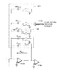
For the analog stages of the adaptive E-A modulator in Fig.7, standard
Switched-
Capacitor (SC-) technology may be used, as shown in Fig. 10, in accordance
with one
embodiment of the system. The 9-bit DAC 1001 is composed of an array of 8
binary
weighted capacitors CDAC, 2CDAC, 4CDAC, 8CDAC, 16CDAC, 32CDAC, 64CDAC, and
128CDAC. The analog input signal is processed by the input sampling stage
1003.
Charge- and discharge operations of the arrays 1001 and 1003 are digitally
controlled by
DAC-Switching control signals 1002 and Input-Switching control signals 1004,
which
are generated in the digital part of the modulator. Together with the
operational amplifier
1006 and the accumulation capacitor 1005, a typical subtract-and-accumulated
operation
can be described as follows. Each E-A clock period is subdivided into two
sections of
roughly equal length, the "sampling-section" and the "accumulation-section".
During the
"sampling-section", all capacitors in 1001 and 1003 are disconnected from the
operational
amplifier. The switches at the capacitors are set such that a charge Qin(n)
proportional to
the input signal x(n) is stored to 1003, and a charge QDAC(n) proportional to
the
(negative) overall feedback signal -[z(n)+w(n)] is stored to 1001 (cf. Fig.7).
Note that in
practical implementation, input signal x(n) and the overall feedback signal
z(n)+w(n )
may be referred to a constant potential, such as V fe f/2. During the
"accumulation-
section", the ports of the capacitors in 1001 and 1003 are switched such that
the
capacitors are discharged and the sum of the charges Q;n(n)+QDAC(n) is forced
to flow
into the accumulation capacitor 1005. Thus, the charge in capacitor 1005 is
changed by
Qin(n)+QDAC(n). The sign of the new potential at the output of the operational
amplifier
13
CA 02540146 2006-03-24
WO 2005/031980 PCT/IB2003/004846
referred to Vref/2 is sensed by the comparator 1007, and clocked into flip-
flop 1008 at the
end of the "accumulation-section". Note that for proper operation both, charge-
accumulation and the sign-sensing have to be finished within the "accumulation-
section",
and therefore the response time of the comparator has to be shorter than 50%
of a E-i
clock period.
The adaptive E-A modulator imposes harsh requirements on the comparator 1007.
The enhanced input dynamic range causes an equally enhanced dynamic range of
the
signal at the output of amplifier 1006, which applies at the comparator input.
For
example, consider a comparator input signal range of a non-adaptive modulator
of +/-1V.
The corresponding range for an adaptive modulator with a 9-bit DAC is +/-IV
for the
largest value of c(n), and +/-3.9mV for the smallest value of c(n). However,
to achieve
the desired and theoretically predicted SNR for the +/-1V-range and +/-3.9mV
range, the
switching behavior of the comparator has to be equal for both cases.
Unfortunately,
comparators tend to become slower as the input signal differences get smaller,
and
signals in the +/-3.9mV range are adversely affected. Thus, it has to be
ensured that the
comparator is sufficiently fast to track very small input signals.
In accordance with one embodiment of the invention, one way to reduce the
dynamic range of the comparator input signal is explained with the help of
Fig. 11. Here,
the accumulation capacitor 1005 of Fig.10 is replaced by an SC-array 1101 of
capacitors
CACC, CACC, 2CACC, 4CACC, 8CACC, 16CACC, 32CACC, 64CACC, and 128CACC. The size
of
the feedback capacitor is adapted to the instantaneous input signal power. An
overall
feedback capacitance CACC,TOT(n) is realized by switching a particular number
of single
capacitors in parallel. If the power of the input signal is small, the mean
charge across
the accumulation capacitor will also be comparatively small. Thus, a smaller
overall
feedback capacitance CACC,TOT(n) can be selected, resulting in a larger
voltage across the
capacitor. On the other hand, an input signal with high power requires a large
overall
feedback capacitance CACC,TOT(n) to keep the accumulation signal within
specified
ranges. The adaptation is carried out in the "sampling-section" of a E-0 clock
period, i.e.,
the preparation of charges Q;,,(n) in 1003 and QDAC(n) in 1001 is not
affected, since 1003
and 1001 are not connected to the operational amplifier. Two cases can be
distinguished,
(1) an uncharged capacitor is added to the configuration CACC,TOT(n) of the
previous clock
period, and (2) a capacitor is removed from the instantaneous configuration
CACC,TOT(n)=
The two cases are explained with the help of capacitor 1105 and the associated
switch-
14
CA 02540146 2006-03-24
WO 2005/031980 PCT/IB2003/004846
array 1106 for clock period number (n+1). One port of each capacitor in the
array 1101 is
permanently connected to the inverting input of amplifier 1103.
Case (1): An uncharged capacitor 1105 can be added to the active array
CACC,TOT(n) by configuring 1106 such that the second port is connected to the
amplifier
output during the whole period number (n+l). This causes a redistribution of
the charges
Q ACC (n)
and a thus a change in the voltage UACC, i.e., it changes from CACC,TOT(n) to
QACC (n)
CACC,TOT (n) + 2CACC , where QACC(n) is the charge in array 1105 at the end of
the clock
period number n and in the "sampling-section" of period number (n+l). The
magnitude of
UACC is decreased in this case, since the overall capacitance
CACC,TOT (n + 1) = CACC,TOT (n) + 2CACC has been increased at a constant
charge.
Case (2): Removing capacitor 1105 from the active array CACC,TOT is achieved
by
switching 1106 such that the second port is connected to the reference voltage
Vref/2
during the whole period number (n+l). Since this potential is equal the
virtual potential
of the inverting input of amplifier 1103, the amplifier forces the output to
change its
QACC(n) QACC(n)
potential from CACC,TOT (n) to CACC,TOT (n) - 2CACC . As above, QACC(n) is the
charge in
array 1105 at the end of the clock period number n and in the "sampling-
section" of
period number (n+1). The magnitude of UACC is increased in this case, since
the overall
capacitance CACC,TOT (n + 1) = CACC,TOT (n) - 2CACC has been decreased at a
constant
charge.
In various embodiments of the invention, the adaptation of CACC,TOT(n) is
achieved based, at least in part, on digital signal co(n). An example of an
adaptation
scheme is summarized in Table 2 for an 8-bit signal co(n). Here, the first non-
zero bit
within co(n) is directly used to define CACC,TOT(n). Note that the exact value
of
CACC,TOT(n) is not critically important. In various embodiments of the
invention, the
adaptation algorithm ensures that (1) on average, the magnitude of voltage
UACC is
maximized, but the instantaneous value of UACC does not exceed specified
limits at no
time instant, and (2) the switching between different configurations of 1101
is performed
without any significant loss of charge, and preferably no loss of charge. Loss
of charge
in 1101 results in accumulation errors and thus reduces the system
performance.
15
CA 02540146 2006-03-24
WO 2005/031980 PCT/IB2003/004846
Table 2: Example of an adaptation scheme for Q-switching
Bit pattern co(n) Overall capacitance CACC,TOT(n)
[l x x x x x x x] 128CACC
[0 1 xxxxxx] 64CACC
[0 0 1 x x x x x] 32CACC
[0 0 0 1 xxxx] 16CACC
[0 0 0 0 1 x x x] 8CACC
[0 0 0 0 0 l x x] 4CACC
[0 0 0 0 0 0 1 x] 2CACC
[00000001] CACC
The above-described manner for reducing the dynamic range of the comparator
input signal may be applicable to a wide variety of adaptive and non-adaptive
E-i
modulators, and is not limited to an adaptive E-0 modulator in which the
adaptation stage
tends to keep the instantaneous magnitude of the analog feedback signal z(n)
within the
first range [-a, +a] and greater than the analog input signal's x(n)
instantaneous
magnitude.
Alternative embodiments of the invention may be implemented as a computer
program product for use with a computer system. Such implementation may
include a
series of computer instructions fixed either on a tangible medium, such as a
computer
readable media (e.g., a diskette, CD-ROM, ROM, or fixed disk), or fixed in a
computer
data signal embodied in a carrier wave that is transmittable to a computer
system via a
modem or other interface device, such as a communications adapter connected to
a
network over a medium. The medium may be either a tangible medium (e.g.,
optical or
analog communications lines) or a medium implemented with wireless techniques
(e.g.,
microwave, infrared or other transmission techniques). The series of computer
instructions embodies all or part of the functionality previously described
herein with
respect to the system. Those skilled in the art should appreciate that such
computer
instructions can be written in a number of programming languages for use with
many
computer architectures or operating systems. Furthermore, such instructions
may be
stored in any memory device, such as semiconductor, magnetic, optical or other
memory
devices, and may be transmitted using any communications technology, such as
optical,
infrared, microwave, or other transmission technologies. It is expected that
such a
16
CA 02540146 2006-03-24
WO 2005/031980 PCT/IB2003/004846
computer program product may be distributed as a removable medium with
accompanying printed or electronic documentation (e.g., shrink wrapped
software),
preloaded with a computer system (e.g., on system ROM or fixed disk), or
distributed
from a server or electronic bulletin board over the network (e.g., the
Internet or World
Wide Web).
Although various exemplary embodiments of the invention have been disclosed,
it should be apparent to those skilled in the art that various changes and
modifications
can be made which will achieve some of the advantages of the invention without
departing from the true scope of the invention. These and other obvious
modifications
are intended to be covered by the appended claims.
17