Note : Les descriptions sont présentées dans la langue officielle dans laquelle elles ont été soumises.
CA 02543450 2006-04-19
WO 2005/043669 PCT/US2004/034266
-1-
FERROELECTRIC VARACTORS SUITABLE FOR CAPACITIVE
SHUNT SWITCHING
The present invention relates to ferroelectric varactors, and in particular,
to
a ferroelectric varactor that is suitable for a capacitive shunt switch.
Electrically tunable microwave filters have many applications in microwave
systems. These applications include local multipoint distribution service
(LMDS),
personal communication systems (PCS), frequency hopping radio, satellite
communications, and radar systems. There are three main kinds of microwave
tunable filters, mechanically, magnetically, and electrically tunable filters.
Mechanically tunable filters are usually tuned manually or by using a motor.
They
suffer from slow tuning speed and large size. A typical magnetically tunable
filter
is the YIG (Yttrium-Iron-Garnet) filter, which is perhaps the most popular
tunable
microwave filter, because of its multioctave tuning range, and high
selectivity.
However, YIG filters have low tuning speed, complex structure, and complex
control circuits, and are expensive.
One electronically tunable filter is the diode varactor-tuned filter, which
has a
high tuning speed, a simple structure, a simple control circuit, and low cost.
Since
the diode varactor is basically a semiconductor diode, diode varactor-tuned
filters
can be used in monolithic microwave integrated circuits (MMIC) or microwave
integrated circuits. The performance of varactors is defined by the
capacitance
ratio, Cmax ~Cmin~ frequency range, and figure of merit, or Q factor at the
specified
frequency range. The Q factors for semiconductor varactors for frequencies up
to
2 GHz are usually very good. However, at frequencies above 2 GHz, the Q
factors
of these varactors degrade rapidly.
Since the Q factor of semiconductor diode varactors is low at high
frequencies (for example, <20 at 20 GHz ), the insertion loss of diode
varactor-
tuned filters is very high, especially at high frequencies (>5 GHz ). Another
problem associated with diode varactor-tuned filters is their low power
handling
CA 02543450 2006-04-19
WO 2005/043669 PCT/US2004/034266
_2_
capability. Since diode varactors are nonlinear devices, larger signals
generate
harmonics and subharmonics.
Varactors that utilize a thin film ferroelectric ceramic as a voltage tunable
element in combination with a superconducting element have been described.
For example, U.S. Pat. No. 5,640,042 discloses a thin film ferroelectric
varactor
having a carrier substrate layer, a high temperature superconducting layer
deposited on the substrate, a thin film dielectric deposited on the metallic
layer,
and a plurality of metallic conductive means disposed on the thin film
dielectric,
which are placed in electrical contact with RF transmission lines in tuning
devices.
Another tunable capacitor using a ferroelectric element in combination with a
superconducting element is disclosed in U.S. Pat. No. 5,721,194.
With the advent of microelectromechanical system (MEMS) technology,
attention has been focused on the development of MEMS devices for radio
frequency (RF) applications. MEMS switches are one of the most prominent
micromachined products that have attracted numerous research efforts in
numerous years and have many potential applications such as impedance
matching networks, filters, signal routing in RF system front-end and other
high
frequency reconfigurable circuits. MEMS switches provide many advantages over
conventional electromechanical or solid-state counterparts in terms of low
insertion loss, high isolation, low power consumption, high breakdown voltage,
high linearity and high integration capability. The majority of today's MEMS
switches employ electrostatic actuation and require a high actuation voltage,
a
major drawback of this type of switch. Recently, high relative dielectric
constant
Barium Strontium Titanium Oxide (BST) thin-films have been used in RF MEMS
switches as a dielectric layer for reducing the actuation voltage requirements
as
well as improving isolation. Isolation can be improved more than 10 dB using
ferroelectric thin-films of BST compared to dielectric materials such as
S13N4.
However, RF MEMS switches have several limitations such as, for example,
relatively low speed, low power handling capability, required high actuation
voltage, low reliability, low switching lifetime and high packaging cost.
Although
improvements are being made in these areas, challenges remain for commercial
CA 02543450 2006-04-19
WO 2005/043669 PCT/US2004/034266
-3-
applications of RF MEMS switches. A ferroelectric varactor based capacitive
shunt switch can over come most of the limitations of existing RF MEMS
switches.
It is against this background that the present invention is based on a
coplanar waveguide (CPW) transmission line shunted by a ferroelectric
varactor.
The novelty in the implementation comes from the elimination any moving parts
for switching and from the elimination of via connections. High resistivity
silicon
with a Si02 layer and a metallic layer deposited on top is used as the
substrate.
The substrate can be any low-loss microwave substrate such as, for example,
Saphire, magnesium oxide, lanthanum aluminate, etc. A ferroelectric thin-film
layer is deposited on a patterned bottom metal layer (metal1 layer) for the
implementation of the varactor. A top metal electrode (metal2 layer) is
deposited
on the ferroelectric thin-film layer, and patterned to form a CPW transmission
line,
such that an overlapping area of the center conductor of the CPW in metal1 and
the shorting line in metal2 layers defines the varactor area. By using the
large
area ground planes in the metal2 layer as well as the metal1 layer, a series
connection of the ferroelectric varactor with the large capacitor defined by
the
ground planes on the top and bottom metal layers was created. The large
capacitor acts as a short to ground, eliminating the need for any vias. The
concept of switching ON and OFF state is based on the dielectric tenability of
the
BST thin-films.
Accordingly, it is an object of the present invention to create a varactor
shunt switch with improved isolation and insertion loss with reduced bias
voltage.
It is another object of the present invention to create a varactor shunt
switch with lower bias voltage requirement, high switching speed, ease of
fabrication and high switching lifetime.
Other objects of the present invention will be apparent in light of the
description of the invention embodied herein.
The following detailed description of specific embodiments of the present
invention can be best understood when read in conjunction with the following
drawings, where like structure is indicated with like reference numerals and
in
which:
CA 02543450 2006-04-19
WO 2005/043669 PCT/US2004/034266
-4-
Fig. 1 illustrates a cross-sectional view of the multiple layers of the
capacitive
shunt switch according to one embodiment of the present invention.
Fig. 2a is a pattern of the bottom metal electrode according to one
embodiment of the present invention.
Fig. 2b is a pattern of the top metal electrode according to one embodiment
of the present invention..
Fig. 2c is a top-view of a varactor according to one embodiment of the
present invention.
Fig. 2d is a cross-sectional view of the varactor area according to one
embodiment of the present invention.
Fig. 3 illustrates a top view of the capacitive shunt switch according to one
embodiment of the present invention.
Fig. 4 represents the electric circuit model of the varactor shunt switch of
Fig.
3 according to one embodiment of the present invention.
Fig. 5 illustrates simulated isolation using different dielectric constants
with
the same varactor area according to one embodiment of the present invention.
Fig. 6 illustrates simulated insertion loss using different varactor areas
with
the same dielectric constant according to one embodiment of the present
invention.
Fig. 7 illustrates simulated isolation and insertion loss of the varactor
shunt
switch for an optimized device according to one embodiment of the present
invention.
Fig. 8 illustrates experimental measurements on the varactor shunt switch
according to one embodiment of the present invention.
Fig. 9 illustrates experimental results versus the simulation results for the
varactor shunt switch according to one embodiment of the present invention.
In the following detailed description of the preferred embodiments,
reference is made to the accompanying drawings that form a part hereof, and in
which are shown by way of illustration, and not by way of limitation, specific
preferred embodiments in which the invention may be practiced. It is to be
CA 02543450 2006-04-19
WO 2005/043669 PCT/US2004/034266
-5-
understood that other embodiments may be utilized and that logical, mechanical
and electrical changes may be made without departing from the spirit and scope
of the present invention.
The concept of implementing shunt capacitance will be useful for a large
number of MMICs such as, for example, tunable one-dimensional and two-
dimensional electromagnetic bandgap (EBG) structures, tunable band-reject and
.
bandpass filters, interference suppression systems, microwave switching
applications, distributed phase shifters for microwave and millimeterwave
frequencies. Furthermore, the present invention is also suitable for two-
dimensional and three-dimensional EBG arrays. In addition, these switches
could
be used in analog and digital applications, such as, for example, interlayer
coupling in multi-layered packages, isolation of specific subsystems with a
larger
system. This type of switch could also serve as a sensory element, since
ferroelectric thin-films manifest piezo-electricity (useful for pressure
sensors,
accelerometers, etc.), pyroelectricity (for infra-red detectors), and electro-
optic
activity (voltage induced refractive index change for color filters, displays,
optical
switching, etc.).
Fig. 1 illustrates a cross-sectional view of the multiple layers of the
varactor
shunt switch. The varactor shunt switch is designed on CPW transmission line
10
with a multilayer substrate. A tunable ferroelectrical thin-film of BST 20
with a high
dielectric constant (Er >_ 100) is used as a dielectrical layer (400 nm
thickness) on
top of the platinum/gold layer 25 with a thickness of 500 nm. A titanium
adhesion
layer 30 of 20 nm is deposited between the platinum/gold layer 25 and the
silicon
oxide/high resistivity silicon substrate layer 35 and 40. The silicon has
resistivity of
> 1 k~2-cm and is typically about 6 k~-cm. The thickness of the silicon oxide
layer
and the high resistivity silicon substrate 40 are 200 nm and 20 mils
respectively.
As a first step in the process, a patterned bottom electrode (metal1 layer) is
processed on a Si/Si02 substrate by electron-beam (e-beam) deposition (or
30 sputtering) and lift-off photolithography technique. Fig. 2a shows the
pattern of the
bottom metallic layer 25. After the lift-off photolithography process for the
CA 02543450 2006-04-19
WO 2005/043669 PCT/US2004/034266
-6-
platinum/gold layer 25, the layer 25 is covered by a 400 nm ferroelectric thin
film
20 such as, for example, barium strontium titanate (BST), strontium titanate
(STO)
or any other non-linear tunable dielectric, using a pulsed laser ablation
(PLD)
process or by RF sputtering. Note that the ferroelectric thin-film can be used
in the
paraelectric state or in the ferroelectric state to optimize the switch
performance
based on the type of application.
Fig. 2b illustrates the pattern of the top metal electrode 15 that is
deposited
on top of the ferroelectric thin film 20. This top metal electrode 15 is
comprised of
gold and includes the central signal strip 100 and the ground conductors 110
of
the CPW. The top metal electrode 15 is prepared by e-beam deposition (or
sputtering) and lift off photolithography process. The ground conductors in
the
bottom metallic layer 25 and top metal electrode 15 are effectively shorted,
due to
the large capacitance between these two layers, eliminating need for the via
holes.
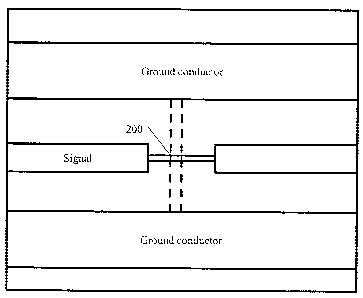
The top view of the finalized CPW is shown in Fig. 2c. In Fig. 2c, the
varactor
area 200 is defined by the overlap area between the top metal electrode and
the
metallic layer indicated by the dashed lines. The bottom metallic layer 20
comprises two ground conductors with exactly the same dimensions as the CPW
ground lines and a shunt conductor, connecting the two ground lines in the
metal1
layer, seen as the dotted lines in Fig. 3. When the capacitance of the
varactor is
very high (at OV bias), the signal is coupled through the varactor and passes
through the shunt conductor to the ground. The varactor capacitance is in
series
with the larger capacitance introduced by the overlapping of the ground
conductors in the top metal electrode (metal2) and the bottom metallic layer
(metal1 ). The output is isolated from the input because of the signal being
shunted to ground at OV, resulting in the OFF state of the device. When one
applies a do voltage to the center conductor of the CPW in the metal2 layer,
the
dielectric constant of the ferroelectric thin-film is reduced and results in a
lower
varactor capacitance. When the varactor capacitance becomes small, the
majority
of signal from the input will be passed on to the output, because of reduced
CA 02543450 2006-04-19
WO 2005/043669 PCT/US2004/034266
coupling by the varactor, resulting in the ON state of the device. Large
dielectric
tenability results in high isolation and low insertion loss of the device.
In the cross section of the varactor, see Fig. 2d, the widths of the two
overlapping top metal electrode 15 and bottom metallic layer 25 are chosen
such
that a required value of capacitance is obtained based on the known relative
permittivity (sr) of the ferroelectric thin-film. Tuning is obtained if a DC
electric field
is applied between the ground conductors and the central signal strip of the
CPW
(using CPW probes). The DC field changes the relative permittivity of
ferroelectric
thin-film, and hence the capacitance of the varactor.
In one embodiment, the width of the center signal strip of the CPW and the
spacing between the center signal strip and ground conductors were chosen so
that the characteristic impedance is close to about 50 S2 and the line losses
are
minimized. The CPW line has the dimensions of Ground-Signal-Ground being
150 pm/50 pm/150 pm for DC-20 GHz on the high resistivity silicon substrate
35.
The spacing (S) between the center signal strip and ground conductors is taken
as 50 pm and the geometric ration (k = W/(W + 2S)) is equal to 0.333 of the
CPW
line. The device area is approximately 450 pm by 500 pm. The varactor area,
which is the overlap of the top metal electrode and the bottom metallic layer
is
approximately 75 pm~.
The simple circuit implementation as the present invention is compatible with
Si MMIC technology, wherein the need for vias is eliminated in this two metal
layer
process. The switch is in the normally "OFF" state compared to MEMS capacitive
shunt switches which are in the normally "ON" state. In addition, these
switches
are capable of switching at ~30 ns switching speeds, where as the MEMS
switches are slower (~10 ps). Further, a lower bias voltage (<10V) can be used
compared to MEMS (40-50V) for switching. The varactor shunt switch can be
designed for a bias voltage of less than 2 V.
The design trade between the isolation (OFF-state) and insertion (ON-state)
loss depends on the varactor area and the dielectric constant of the BST thin-
films. Large varactor area and high dielectric constant are required to get
the high
CA 02543450 2006-04-19
WO 2005/043669 PCT/US2004/034266
_g_
isolation but it will increase the insertion loss. To keep the insertion loss
at a
minimum (<1 dB), the optimized overlapping area and dielectric constant are
taken as 25 pmt and 1200 respectively.
Fig. 4 represents the electric circuit model of the varactor shunt switch of
Fig.
3. The electrical circuit model is obtained by shunting the varactor, with L
400 and
Rs 410 being parasitic inductance and resistance respectively. The shunt
resistance Rd 430 models the lossy (leakage conductance) nature of the
varactor.
The varactor capitance 420 can be obtained by the standard parallel plate
capacitance calculation, with the dielectric permittivity of the BST thin-
film, and the
overlap area of the center signal strip and the shunt line. The varactor
capacitance
is given by:
Cv= ~o. s,~. A/t (1 )
Where Eo is the dielectric permittivity of free space, E,~ is the relative
dielectric
constant of the ferroelectric thin-film used, A is the area of the varactor,
and t is
the thickness of the ferroelectric thin-film.
The series resistance (Rs) 410 of the shunt conductor line in the bottom
metal layer (metal1 ), where the signal is shunted to ground is calculated
using
Equation 2
R = I /(Q wt) (2)
where, o' is the conductivity of metal used in the top metal electrode, w is
the width
of the conductor, I is the length of the line shunting to ground, and t is the
thickness of the conductor.
The inductance 400 (L) of the line is calculated using Equation (3)
L = (Zo/(2rrf))sin(2rrl/ l~g) (3)
CA 02543450 2006-04-19
WO 2005/043669 PCT/US2004/034266
-9-
where, Zo is the characteristic impedance of the CPW transmission line, f is
the
operating frequency, and Ag is the guide-wavelength.
The shunt resistance 430 (Rd) of the varactor can be calculated using
Equation (4)
Rd(V) = 1/(c~C(V) tanb) (4)
where, C(V) 420 is the capacitance of the varactor and tanb is the loss-
tangent of
the ferroelectric thin-film.
The performance (e.g., high isolation, low insertion loss, etc.) of the
capacitive shunt switch depends on the dielectric tunability of the
ferroelectric thin-
film. High capacitance value will increase the isolation in the OFF-state but
it will
also increase the insertion loss in the ON-state. The capacitance value can be
increased by using a high dielectric constant of the ferroelectric thin-films
or large
varactor area. Increasing the dielectric constant of the ferroelectric thin-
films with
same varactor area does not change the isolation very much but the resonance
frequency decreases due to the increased varactor capacitance, see Fig 5. Fig.
5
shows the isolation for the relative dielectric constants of 2000, 1500, 1200
and
1000 from left to right with a fixed varactor area of 5 x 5 pmt.
Further, insertion losses increase with increasing varactor area as shown in
Fig. 6. Fig. 6 illustrates the insertion loss for a fixed dielectric constant
of value
200 with the varactor areas of 15 x 15 pmt, 10 x 10 pmt, 10 x 5 pmt, and 5 x 5
pmt from left to right.
The simulated optimized dielectric constant of ferroelectric thin-films is
taken as 1200 for the OFF-state and 200 for the ON-state with a varactor area
of
5 x 5 pmt, or 25 pmt. Fig. 7 illustrates the simulated isolation and insertion
loss of
the varactor shunt switch for the optimized device. The isolation of the
device is
better than 30 dB at 30 GHz and the insertion loss is below 1 dB below 30 GHz.
The varactor shunt switch was tested using a HP 8510 Vector Network
Analyzer (VNA). A Line-Reflect-Reflect-Match (LRRM) calibration was performed
over a wide frequency range (5 to 35 GHz). The sample was then probed using
CA 02543450 2006-04-19
WO 2005/043669 PCT/US2004/034266
-10-
standard GSG probes. The do bias was applied through the bias tee of the VNA.
Fig. 8 illustrates the experimental measurements performed on the varactor
shunt
switch for 0 V (i.e., the OFF state) and for 10 V do bias (i.e., the ON
state). In the
measured device, the capacitance of the varactor at zero bias was about 0.85
pF
and was reduced to about 0.25 pF for a bias voltage of 10 V, thereby,
resulting in
a dielectric tunability of more than 3:1.
Fig. 9 illustrates the experimental results obtained from the varactor shunt
switch compared to the simulation results based on the electrical model
developed for the device. The experimental results were obtained up to 35 GHz.
Theoretical simulations performed on the same device indicates that the
isolation
(off-state S21 ) improves to 30 dB near 41 GHz. A good agreement between the
theoretical and experimental results over the frequency range of measurements
can be seen as shown in Fig. 9. Therefore, the experimental data confirms the
operation of the varactor shunt switch for microwave switching applications.
Table 1 demonstrates the comparison among solid-state switching devices,
RF MEMS and the ferroelectric-based varactor shunt switch. The advantages of
the varactor shunt switch include lower bias voltage requirement, high
switching
speed, ease of fabrication and high switching lifetime.
Table 1 _ _
Device Solid state RF MEMS Ferroelectric
characteristics switches capacitive shuntvaractor based
and performance switches shunt switch
parameter
Type of switch Normally OFF Normally ON Normally OFF
or
ON
Actuation volts Low 3-8 V Hi h 40-50 V Low <10 V
a
Switchin speed Hi h 5-100 ns) Low (~ 10 ps) High <100 ns)
Isolation (dB) <20 db @ 20 Very high (>40 High (>20 dB
GHz dB @
30 GHz 30 GHz
Insertion loss >1 db @ 30 GHz Very low (<1 Low (<1.5 dB
(dB) db @ @
30 GHz 30 GHz
Switchin lifetimeHi h Low Hi h
Packs in cost Low Hi h Low
Power handlin Poor 0.5 - 1 Medium < 5W Hi h > 5 W
W
Power Low 1-20 mW) Almost zero Almost zero
CA 02543450 2006-04-19
WO 2005/043669 PCT/US2004/034266
-11-
consumption (OFF-
state
Breakdown volts Low Hi h Hi h
a
DC resistance Hi h 1-5 ~ Low <0.5 S2) Low <0.5 i2)
Linearit Low Hi h Hi h
IP3 Low ~+28 dBm Hi h ~+55 dBm Not available
Integration Very good Very good Very good
capability
Note that the ferroelectric varactor shunt switch performance predicted in
the table are based on theoretical calculations.
It is noted that terms like "preferably," "commonly," and "typically" are not
utilized herein to limit the scope of the claimed invention or to imply that
certain
features are critical, essential, or even important to the structure or
function of the
claimed invention. Rather, these terms are merely intended to highlight
alternative or additional features that may or may not be utilized in a
particular
embodiment of the present invention.
Having described the invention in detail and by reference to specific
embodiments thereof, it will be apparent that modifications and variations are
possible without departing from the scope of the invention defined in the
appended claims. More specifically, although some aspects of the present
invention are identified herein as preferred or particularly advantageous, it
is
contemplated that the present invention is not necessarily limited to these
preferred aspects of the invention.