Note : Les descriptions sont présentées dans la langue officielle dans laquelle elles ont été soumises.
CA 02552915 2006-07-07
WO 2005/068965 PCT/BR2005/000004
1
SYSTEM AND METHOD FOR MEASUREMENT OF OPTICAL
PARAMETERS AND CHARACTERIZATION OF MULTIPORT OPTICAL
DEVICES
Background of the Invention
S The present invention relates to the interferometric measurement
of optical devices parameters including the determination of the "S"-
parameters of optical devices with one or more ports, in transmission
and/or reflection.
"S"-Parameters are concepts widely used in the microwave
engineering practice, which facilitate the analysis of the signal transfer
between the ports of a rnulti-port device, therefore, its application is
also feasible in optical device techniques. However, while based on
similar principles, optical "S"-parameters differ substantially from
microwave "S"-parameters due to the fact that the polarization
characteristics of the light transmitted through the DUT (Device Under
Test) must be taken into account. In the case of microwave "S"-
parameters, each "S~' is a complex number that represents the
characteristics of transmission and/or reflection from port Y to port X
of the DUT. In the case of optical "S"-parameters, each "S~' it is
represented using the Jones' formalism (Jones matrix) and/or the
Miiller's formalism (Miiller matrix). From each "Sxy" it is possible to
deduct all the usual optical properties for the characterization of
photonic devices, such as: bandwidth, phase, time delay, chromatic
dispersion, 2nd order chromatic dispersion, reflectance, reflection
coefficient, transmittance from port "y" to port "x" and vice-versa,
transmission coefficient from port "y" to port "x" and vice-versa,
insertion loss, polarization dependent loss, polarization mode
dispersion (DGD/PMD), 2nd order DGD, etc.
I~e~cription of the previous art
Optical components have become increasingly important in
CA 02552915 2006-07-07
WO 2005/068965 PCT/BR2005/000004
2
WDM systems (Wavelength Division Multiplexing), high capacity optical
systems, a11-optic communications systems, dispersion compensation,
filer sensing and other technologies. In the last twenty years, a
significant amount of research has been focused on the development of
optical devices equivalent to electronic components, in order to allow
the development of all-optical neturorks and of the photonics field in
general. The full utilization of the benefits of such devices, requires the
accurate measurement of their optical characteristics, such as:
bandwidth, phase, time delay, dispersion, reflectance, transmittaiice,
insertion loss, polarization dependent loss, polarization mode
~.ispersion etc.. The optical characteristics of the DUT are generally
defined for specific wavelengths, therefore, to extend these
characteristics ewer a certain bandwidth, as it is normally the case, the
characterization process should be repeated for a finite number of
wavelengths,
Several equipments, systems and methods have been proposed
to avoid the need of conducting a great number of measurements in
several waveierigths. One well-known process is the so-called "RF
Phase Shift" technique. Such method of characterization of optical
devices demands a set of expensive equipments and entails a trade-off
between precision and resolution of wavelength.
Due to the above mentioned shortcoming, current solutions ua~
anterferometric technidues which have become more efficienty more
accurate and less costly
One known system that employs an interferornetric optical
technique, is described in document EP 1182805. In this arrangement,
a laser generator is swept in wavelength with a constant sweep speed,
its signal being split into two arms, of necessarily different lengths,
whith the DUT inserted in one of them. The signal transmitted through
the "known" arm (called reference arm) and the one which traveled
through the arm with the DUT (Device Under Test) are mixed in a
CA 02552915 2006-07-07
WO 2005/068965 PCT/BR2005/000004
3
photodetector, giving rise to an electric signal from the beating of the
different frequencies of optical signals, the displacement between said
frequencies being due to the propagation delay in the different signal
paths. The resulting heterodyne (or quasi-homodyne) signal, ranging in
frequency from some KI~z to a few l~fl~z, is directed to a signal
processing system that determines the desired optical characteristics
of the device. This procedure allows the translation of the information
regarding the optical characteristics of the DUT from the optical to the
e~ectrical domain. For example, the instantaneous-wavelength-
dependent coefficient of transmission is given by the instantaneous
amplitude of the heterodyne electrical signal. A considerable
disadvantage of this technique, called SWI (Swept Wavelength
interferometry), is the need to use only "swept" lasers, which ai=r
continuously swept in wavelength. Another shortcoming is the fact that
the lambda noise (wavelength) of the laser is amplified, due to the
required large length imbalance of the interferometer arms.
~'~~sects of the Invention
in view of the above, the first aim of the invention is to provide a
system that allows the complete characterization of multi-port passive
optical devices in a speedy manner, with the feature of being able to
operate both in the continuous sweep swept mode or in the stepped
~vvept modes of the tunable laser source.
It constitutes another purpose of the invention to furnish a
system that provides great precision in the measurements of
transmission coefficient, reflection coefficient, transmitance,
reflectance, intrinsic loss, bandwidth, phase, time delay, chromatic
dispersion, 2nd order chromatic dispersion, differential group delay
(DGD)/polarization mode dispersion, 2nd order DGD, polarization
dependent loss of optical devices, as well as providing high resolution
in wavelength.
Yet another object is to provide a system where the effect of the
CA 02552915 2006-07-07
WO 2005/068965 PCT/BR2005/000004
4
mechanical vibrations is minimized.
Another additional object is to provide a system where the effect
of the variations of ambient temperature is minimized=
t~nother object is to furnish a system and a method that allows
the simultaneous determination of all the above mentioned optical
characteristics in all the transmission directions of a mufti-port DUT,
with a single wavelength sweep of the tunable laser source.
Summary of the Inventions
T he above mentioned aims are attained by means of an
IO interferometric optical arrangement in which the paths of the test
signals (or DUT signals) and the reference signals has approximately
equal lengths, without requiring any length imbalance in the arms of
the interferomeier.
According to another feature of the invention, the optical signal
I S of at least one of the arms of the interferometer is phase- or frequency-
modulated,
In accordance with another feature of the invention, the optical
phase or frequency modulator can be constructed by any known
optical technologies,
20 In accordance with another feature of the invention, the optical
arms of the interferometer can be constructed using different physical
~adis for propagation and conduction of the optical signal, such as:
optical waveguides, planar waveguides, free space (FSO) etc..
Brief Description of the Drawings
25 Additional advantages and features of the invention will be mars
easily understood through the description of some exemplary
embodiments which exemplify the arrangements used in the diverse
kinds of measurements as well as the operating principles of the
system, together with the related figures, in which:
CA 02552915 2006-07-07
WO 2005/068965 PCT/BR2005/000004
Figure t shows the arrangement used in the measurement of the
reflection parameters of a passive component with only one port,
according to the invention.
Figure 2 shows the arrangement used in the measurement of the
5 transmission parameters of a passive component with two ports,
~ccoi~ding to the invention.
Figure 3 illustrates an arrangement used for the partial
characterization of a two-port DUT, simultaneously in transmission
and reflection.
I0 Figure ~ shows an arrangement used in the simultaneous
characterization of all ports, in transmission and reflection, of a two-
port device.
Figures 5 to 8 illustrate the paths of the optical signals in the
characterization of optical "S"-parameters, using the arrangement
I5 shown in the previous figure.
Figure 9 illustrates a block diagram showing the operating
principle for suppressing the effects of vibration and temperature
changes,
Figure 10 illustrates the arrangement used for the above
20 mentioned suppression being applied to the optical circuitry shown in
~~etre 2~.
Figure 11 illustrates the arrangement used for simultaneous
measurement of the polarization characteristics in transmission and
reflection of a 2-port DUT.
25 Deta~i,l,ed description of the Invention
The invention now will be detailed through specific examples
related to some typical applications. The first embodiment refers to an
gerizent used for the characterization of the reflection parameters
of a DUT. Fig. 1 illustrates relative positions of the elements used in
30 the test, to wit;
CA 02552915 2006-07-07
WO 2005/068965 PCT/BR2005/000004
6
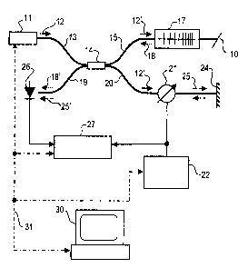
- a trznable laser signal source 11 (TLS - Laser
~'ur~able Source~3 that is controlled by the cor~trol system 30;
- an optical coupler 14;
a device under test 17 (DUTj;
~ an optical modulator 21;
- a signal generator 22;
- an optical fiber mirror 24;
- optical detection system 26
- electronic system for data acquisition 27
i 0 The system shown in Fig. 1, whose optical part forms a
Michelson interferometer, operates in the following way: the control
system 30, which manages the optical characterization process, issues
a command to TLS 11 to generate an optical signal 12. This sigpal is
dr~°ected by the optical fiber 13 to the optical coupler 14, where it
is
' 15 split in two sisals 12' and 12' ' that are directed, through optical
fibers 15 and 20, to DUT 17 and optical modulator 21, respectively.
The signal l2' that impinges on the DUT can be transmitted or be
reflected, depending of its wavelength and the specific opfr
characteristics of the D~tJT. The transmitted signal is absorbed at
20 output device 10. The reflected signal 18 returns by the optical fiber 15
to coupler 14, where it is split again: part of it returns through optical
fiber t 3' and another part 18', is transmitted by optical fiber 19. In
turn, the signal 12" passes though modulator 21, where it is
modulated in phase or frequency by the modulating signal 23 provided
25 by the signal generator 22. The modulated optical signal 25 is reflected
by mirror 24 and passes again though the modulator 2'I, returning t~
~zptical fiber 20 anti going to the coupler 14, where it is split. The
portion 25' of this modulated signal enters optical fiber 19, that also
transmits signal 18' to the optical detection system 25.
30 The optical detection system 26 produces the heterodyning
CA 02552915 2006-07-07
WO 2005/068965 PCT/BR2005/000004
7
between the two signals 28' and 2~', translating information from the
optical dorr~ain to the electrical domain, giving at ats output, an addition
to the original signals, the products of the heterodyning, particularly
the difference signal. This is an electrical signal whose spectrum
contains frequency components whose amplitude and phases depend
an the modulating signal 23 and on the optical characteristics of the
DUT. The data acquisition circuit 27 extracts information about the
optical characteristics of the DUT from the electrical signal. This
pirocess of extraction of the information contained in the electric signal
~ 0 can be carried through using different techniques, such as filtering
and direct detection, Lock-in, FFT (Fast Fourier Transform] etc, which
can be implemented using analog techniques (analogic processing of
signals), digital (digital processing of signals) and/or through soda.
'the amplitude information extracted from the electric signal is
15 proportional to the characteristic called "reflection coefficient" of DUT
1?. This amplitude information enables the extraction of other
information about the DUT, such as: reflectance, insertion loss,
bandpass etc.. The phase information extracted from the electric signal
refers to the phase deviation introduced by the DUT in the reflected
20 signal, allowing the acquisition of other information, such as: group
delay, chromatic dispersroii ~..
Besides registering the data about the reflection coefficient and
phase deviation of the DUT,. the control system manages the process,
selecting the series of wavelengths, which must be sufficiently close so
25 as to provide a good resolution in the determination of the DUT
chaY~cterisif~.
As already mentioned, the optical phase/frequency modulation
uses any know technique of modulation,. such as for example,
changing the refraction index of an optical element, changes in the
30 signal propagation length, electric-optic effects, etc.. Amongst these,
one exemplary embodiment uses a piezoelectric ceramic cylinder ova
which the optical fiber is wrapped. Applying the modulating signal to
CA 02552915 2006-07-07
WO 2005/068965 PCT/BR2005/000004
8
this cylinder, its dimensions change in accordance with this signal,
stretching the optical fiber which char~g~s its length as mell as its
refractive index, producing the phase modulation in the phase ol' the
optical signal that traverses the fiber.
The optical modulator ~I doesn"t have to be Iocated in the
reference arm of the interferometer. It can alternatively be located in
the DUT arm or in both arms.
The system is not limited to the use of a saw-tooth modulating
signals other waveshapes can be used,. such as squaxe wave,. sine wave,.
I O waves composed of linear segments etc.
One of the advantageous features of the invention is the fact that
the system can work with laser sources in which the wavelength is
continuously changed or where this waveier~gth is changed by ate
~"Swept" and "Stepped" Lasexs).
Fig. 2 illustrates the arrangement used in the measurement
the transmission characteristics of a DUT 17. For clearness sake,
control lines 31 that connect the control system to TLS 11 and to the
electronic acquisition circuitry 2'~ had been omitted in this ~g~,
however such control exists in the same way as in the previous
arrangement. In the arrangement of Fig. 2, whose optical part forms an
Mach-Zehnder interferometer, the signal 12 generated by the laser 13.
conveyed by the optical fiber 13 to the coupler 14, where it splits
,into the signals 12' and 12". The first one of these is transmitted by
optical fiber 15 to the DUT 17, where it can be reflected, spread,
absorbed or even transmitted as signal 41, depending on the specific
optical characteristics of the DUT. The signal 12'~' is d~irectccz tai
modulator 21, where it is modulated by the signal provided by the
signal generator 22, resulting in the phase- or frequency-modulated
signal 25, that it is directed by the optical fiber 33 to a second coupler
3~F 34, where it is added to signal 41 transmitted through DUT 17. Part of
these added signals, 25' and 41', is directed to the optical detection
CA 02552915 2006-07-07
WO 2005/068965 PCT/BR2005/000004
9
system 37, where the heterodyning between this signals occurs. in a
similar way to that shown in the arrangement of Fig. l, the signal
difference is introduced in one of the inputs of the acquisition circuit
27, which receives in its other input the reference signal from the
signal generator, that is used to determine the transmission
characteristics of DUT 17. Devices 10 and 10' are terminations that do
not reflect the signal..
The Fig. 3a illustrates one of the arrangements that can be used
for simultaneous characterization of the DUT in transmission and
~~? reflection. Signal 12 of laser 11 is introduced in the optical coupler 14,
which splits it in two components 12' and I2' ', directed respectively, to
DUT 17 and modulator 21, in which occurs the modulation in phase or
frequency by the modulating signal generated by the signal generator
22. The ~noduiated optical signal 25 is directed to the optical coupler
15 44, where it divides in two components 25' and 25' ', the first one being
transmitted to the optical coupler 16 where it is added to the
transmitted signal 41 through said DUT. This sum of signals is
de-~ected by the optical detection system 43 where the heterodyning
between these signals occurs producing several other signals, that are
20 directed to the first input of the acquisition circuit 47, including the
difference signal (25' - 41). This signal has a frequency spectrum that
contains phase and amplitude information of the DUT for a deterxnir~cc~
wavelength. The second input of the acquisition circuit 47 receives the
modulating signal proceeding from generator 22 to provide a phase and
25 amplitude reference for the circuit operation. In the output 47, it is
possible to get the information concerning the S21 transmission
parameter (transmission of port 1 to the port 2) of the DUT.
The second component 25" of the modulated signal is reflected
by mirror 45 and returns through coupler 44, modulator 21 and
30 coupler 14, where it is added to signal 18 reflected by the DUT. These
signals are directed to the optical detection system 42 whose output
produces, among others, the difference signal (25""' - 18) that is
CA 02552915 2006-07-07
WO 2005/068965 PCT/BR2005/000004
inputted to the acquisition circuit 2~ whose output has the
information of amplitude and phase of the reflected signal, providing
the characterization of the reflection parameter of the DUT (S11).
This arrangement illustrated in the Fi~.3a can be interpreted as
5 being equivalent to the overlapping of two optical interferometers, that
can be better seen in figures 3b and 3c. In the first oize, the optic
part forms an Michelson interferometer, composted by the segments of
optical fiber 13, 15, 19, 20, 32 and 34, the mirror 45, couplers 44 and
14 and the optical modulator 21. Figure 3c shows that the optical
~~ elements used in the measurement of the transmission characteristics
of the DUT forms a Mach-~ehnder interferometer, composted by the
optical fiber segments 13, 15, 20, 32, 33, 41, 35, 36 as well as couplers
14, 44, 16 and the optical modulator 21. It is seen that many elements
of said interferometers are part of both devices. Such is the case of the
optical fiber segments 13, 15, 20 and 32, as well as the couplers 14
and 44 and optical modulator 21. This overlapping - that is meant to
provide the simultaneous measurement of two parameters of the DUT -
i~ possible by using the optical modulation in phase or frequency of the
reference signal, entailing the advantage of making the operation of the
interferometers totally independent of the physical lengths of its
interferometer arms.
For characterization of the two other parameters S 1 ~ and X22
with the arrangement of the Fig.3, it is necessary to invert the position
of the DUT. For the concurrent of both ports of a two port device,
simultaneously in transmission and reflection, the arrangement
illustrated in Fig. 4 must be used. This simultaneous characterization
refers to the determination of the reflection and transmission
parameters of the two-port DUT in all directions of propagation (511,
S21, S22 and S 12), in a single wavelength sweep. In this arrangement,
3f1 two different modulating signals, whose frequencies c~ml and c~~r~,
generated by generator 49 cannot be multiple or have coincident
CA 02552915 2006-07-07
WO 2005/068965 PCT/BR2005/000004
11
harmonics. In this figure, the eiectranic circuit that perfarms the
treatment of the sigx~als detected by the detection system 42 and 43
are grouped in blocks 50 and 50', which are responsible for the
acquisition of the parameters "S 11 and S 12" and "S2~ and S21",
respectively.
The Fig.S shows the paths of the optical signals in the
ehaxacte.ri~atio~n of the reflecta.~ar~ p,a~eters of port 1 (511~ In this
measurement, the signal generated by the Iaser is split by coupler I~4
in two components, the first one being directed, through the optical
I0 fiber 15 and the coupler S4, to the modulator ~~ where it is modulated
in phase or frequency with the modulating signal with frequency c~m1
and going from there to the Pl port of DUT 17. The second component
traverses optical fiber 20 to coupler 52, which forwards part of this
eornpoi~.ei~.t thrr~ugh fiber 53 to coupler 54, where is added to the
1 S reflected signal from the 17UT that returned. through modulator 21.
These added signals traverse optical fiber 55 to the optical detection
system 42, the resulting electric signal of this detection being
processed by block 50, which includes the acquisition circuitry t
allows the characterization of the S11 parameter.
20 The Fig.6 shows the paths of the optical signals for the
characterization of the S21 parameter. In this case, the first component
of the signal produced by the laser is directed through the optical fiber
15 to coupler 54, where it is split: part of this signal goes to the phs<~~
or frequency modulator 21, where is modulated by the modulating
25 signal with frequency c~m1 and traverses DUT 1'7, in the direction from
the P1 port to the P2 port, as well as to modulator 51 where it is
modulated by the modulating signal with frequency com2 and forwarded
to coupler 52, where it is added to the unmodulated signal that arrives
from optical fiber 53. The detection, by the optical detection system 43,
30 of these added signals. produces the difference signal that will be
tre~.ted by the electrpnics circuitry 50', enabling the deterr~~n~.tion of
,, o . ,
CA 02552915 2006-07-07
WO 2005/068965 PCT/BR2005/000004
12
the S2I parameter associated with the transmittance of DUT 17, in the
direction of port Pl port to port P2.
The paths of the optical signals in the characterization of the
reflection parameters in port 2 (S22) are illustrated in the Fig.?. In this
measurement, the optical signal generated by the laser is split by the
coupler 14 in. two components, the second one being directed, throw.
the optical fiber 20 and coupler 52, to the modulator 51 where is
modulated in phase or frequency by the modulating signal with
frequency c~m2 and from there to the P2 port of DUT 17. The first
component leaves coupler I4, traverses optical fiber i 5 to coupler 54,
that sends part of this component through fiber 53 to the coupler 52,
where is added to the signal reflected by the DUT returned thorough
modulator 51. These summed signals traverse optical fiber 56 to the
optical detection system 43, the resultant electric signal of this
I S detection being processed by the block 50' that supplies the data for
the characterization of the S2~ parameter.
The Fig.8 depicts the paths of the optical signals for the
characterization of S 12. In this case, the second signal component
produced by the laser is transmitted through optical fiber 2fl to cc~-~pl
20 52, where it is split. One part of this signal is modulated in phase or
frequency by the optical modulator 51 with frequency v~m2 then
traverses the DUT 17, in the direction of port P2 to port P1, further
averring modulator 21 where this signal is modulated by the
frequency c~ml being directed from there tø coupler S4, where it is
25 added to the unmodulated signal from the optical fiber 53. The
detection of the summed signals by the optical detection system 42
produces the signal difference that will be processed by blocl~ 5~,
enabling the determination of the S12 parameter associated with the
transmittance of DUT 17 in the direction of port 2 to port 1.
30 As occurs in the arrangement of the Fig.3, the present
disposition also is equivalent to the overlapping of diverse optical
CA 02552915 2006-07-07
WO 2005/068965 PCT/BR2005/000004
13
interferometers, that share the same segments of optical fibers. Thus,
in figures 5 grad 7, both ~icheison interferometexs have in common the
ring formed by the segments of optical fibers 15, 20 and 53, as well as
couplers 14, 52 and 54. In the arrangements ~of figures 6 and 8, the
Mach-~elmder interferometers share the optical fbers segments ~~', as.
well as the path that goes from coupler S4, passing by the modulator
21, the DUT 17 and the modulator 51 to the coupler 52.
The arrangement shown uses only two optical detection systems
- 42 and 43 - each one receiving the signals related to two parameters:
I O the signals that allow the determination of the parameters ~j; t and ~~~
are received simultaneously by system 42, and the ones referring to
the parameters S21 and S22 are received simultaneously by the optical
detection system 43. The discrimination between signals that arrive at
the same detection system is possible by the different modulations
applied to these signals. Thus, the signal used. for determination of S11
is modulated by the frequency wml (as shown in Fig.S) while the signal
that allows the determination of S 12 is modulated by the frequencies
wm2 (as shop. in Fig.B). In general, the electronic acquisition circt~
select information in the frequencies of interest, allowing the
discrimination of the different Sxy parameters, even when they are
received by the same optical detection system, because these
~formafiion are individualized by the modulating signals.
According to the invention, the measurements of the
characteristics of the DT,JT's are reached by optical interferometry, in
which the light signals propagate between two different paths or arms
and are later recombined. The results of these measurements are
~hftuerlced by any changes occurring in these paths, such as, for
example, the _refractive index of the fiber, the physical distance covered
by the light etc.. Thermal variations and mechanical vibrations can
stretch the optical fiber or modify its refraction index, affecting
differently the two arms of the interferometer and, consequently,
CA 02552915 2006-07-07
WO 2005/068965 PCT/BR2005/000004
14
introducing detrimental variations in the output signals of fhe
interferometer.
The changes in the properties of the optical paths are neutralized
in the present invention by means of an active control of the changes
in the optical system, which compensates the errors due to thermal
variations and/or mechanical vibrations. This device consists of
virtual duplication of the interferometer, making it to operate in two
distinct wavelengths. A first group of wavelengths is used to
characterize the DUT. A second and fixed wavelength allows the
evaluation of the variations that occurring in the interferometer due to
variation. of temperature and~or mechanical vibrations and feeding,
back the system with a correction sisal that is applied to the
interferometer that characterizes the DUT.
The block diagram that shows the working principle ~f ~h~
I S temperatuxe compensation is depicted in. Fig,9. As illustrated, two
sources of laser light are used, the first one 81 generating the signal in
variable wavelengths ~,S for DUT test, and the second 82 generating a
~ec~ wavelength signal 7~T for the control and compensation of
vibrations and temperature changes. Both signals are introduced in
2~ interferometer 83. At the interferometer output there are two optical
detection systems, the first one 84 being the optical detection system
for characterization of the DUT and the second, 85, for tile monitor.
signal ~,T. This second optical detection system feeds a comparator and
error signal generator block 86. The interferometer receives a negative
25 error signal feedback through the optical modulators. If a variation it7
~e system produced by thermal variation or mechanical vibration
occurs,, this will be compensated by the feedback link 87, and it will
not affect the measurement results,
~i~.10 illustrates the system of temperature compensation in a
30 more detailed form. In this diagram, two laser generators are used, the.
first 11 producing the test signal (variable wavelength] and the second
CA 02552915 2006-07-07
WO 2005/068965 PCT/BR2005/000004
11 F producing the compensation signal (fixed wavelength 7~T falling
outside the test signal wavelengthj. These signals are added in coupler
14, being split in two components that are transmitted by the optical
fibers 15 and 20. Signal 41 that traversed the DUT is split again by
5 coupler 34 and arrives through the fibers 35 and ~5 at the two op~cie
reception systems 37 and 38. The signal 12" traverses modulator 27.
and is also split by coupler 34 following by fibers 35 and 36 to the
optical reception systems 3? and 38. The optical reception system 38
~~s a selective ~.lter 39 tuned to the control wavelength. Therefore, the
a signal produced by photo detection system 38 is only related to the
control wavelength. The temperature compensation signal is directed
to the block 27', which consists of an electronic circuit similar to that
used in the treatment of the measurement signals. As the optical pa~'~s
are flied for ?~T and the control light source also operates in a fixed
1 S wavelength, the photodetected signal should not suffer a phase
change. In case that some change of phase occurs, this will have been
fused by thermal or mechanical disturbances, and can be
compensated in the ,modulators. As the response of the optic system ~,T
is almost identical for the control and measure wavelengths, the
compensation also occurs in the wavelength band of the test device.
Thus, the optical interferometer setup formed by the acquisition ciret~~~
associated to the optical detection systems 38 allows to obtain the
error signal that will be negatively fed back to the interferometer
through the existing optical phase modulators.. On the other hand, the
,~ elements associated with the optical detection systems 3?, the selective
filter 39' for test wavelengths and the acduisition circuit 2? operate in
the characterization of tie DUT like the previously detailed
arrangement of Fig.2.
Figure 11 bows the device conf guration that allows tl~~
simultaneous determination of the polarization characteristics of the
DUT for two orthogonally polarized light waves. The test signal
generated by the tunable laser 11 is split by coupler 14 in two
CA 02552915 2006-07-07
WO 2005/068965 PCT/BR2005/000004
16
components and directed by the optical fibers 310 and 111 to coupler
112 and 113 where they are split again. The sub-components derived
from coupler 112 are modulated in phase or frequency by the
modulators 114 and 116 with modulating signals cus and cep. The
moc~u~ated signals are processed by the polarization controllers (PC)
115 and 11?, which maximize the orthogonal polarization components
of light s and p, respectively. These signals are summed in the
polarization combiner (PBC - Polarization Beam Combiner) 118, that
guarantees the orthogonality between both and then clirectec~
coupler i i9, where the sum of the signals is split in two components,
directed through couplers 121 and 122 to DUT 125. In this path, each
component of the sum of the signals is modulated by the modulating
signals cal and r~2. Part of these components traverse DUT 125 and
part are reflected by it. Each one of these parts undergo then a second
I5 rnaduiation by the modulating signals ~ 1 or ~2, as the case be. The
resultant signals are then diverted by couplers 121 and 122 and
directed to the Polarization Bean Sputter (PBS) 126 and 1~? and ire
there to the optical detection systems 128, 132, 133 and 135, followed
by the processing and acquisition systems. The modulations suffered
0 by the optical signal during its passage through the modulators allow
e~ f~enfify tlae individual polarization components in quadrature,
allowing the determination of the DLTT polarization characteristics. For
example, the optical signal that arrives at the optical detection system
128 is modulated by the following frequencies, related to the
25 transmission. through the ~~.3
'mss+~2~'~1
'~p~~2~~1
~c~s-cep-~c~2~-~1
As concerns the reflected signal, the optical signals that arrive at
30 the optical detection system 128 are modulated by the following
CA 02552915 2006-07-07
WO 2005/068965 PCT/BR2005/000004
17
frequencies:
i~g+'~G_T~
~u~p+2c~1
~ws_~p+2~1
These 6 signals can be electronically separated and sari be
andividually analyzed by the eleEtronic circuits.
The electronic circuit 129, the optical detection system 125, the
circuit 131 associated to the optical detection system 132 form a
polarization diversity receiver, capable of extracting the amplitude and
phase information of the components and allowing the selective optical
~haracter~ation ~f tl~e S l t and S 12 pareter~n The other ~opdeal
detection systems and the associated circuitry operate in a similar
way, providing the selective polarization characterization of all
parameters of the DUT, namely 511, 5~.2, S~2 and 521.. l3edicated
computational algorithms correlate the information acquired by the
electronic circuits 129, 131, 134 and 136 and allow the complete
characterization of the DUT, as well as the polarization characteristics
of the device, the whole process being carried out simultaneously in a
single wavelength sweep of the Tunable Laser Source_
The measurement technique described previously exemplifies the
characterization of two-port optical devices, generating 4 optical "S"-
parameters (two of reflection and two of transmission). This concept
may be extended, without any loss of generality, to the characterization
of N-ports devices. In this case, taking the most complete version (Fig.
11) the setup "DUT + modulators" (123, 124 and 125) is substituted by
a DUT of N ports (N = 3, 4, 5...) where in each port is inserted an
optical modulator whose frequency is distinct and not multiple of the
remaining ones. Optical couplers sum all these signals proceeding from
the diverse ports of the DUT forwarding these to the couplers 121 and
122, which transmit said summed test signals as well as the reference
CA 02552915 2006-07-07
WO 2005/068965 PCT/BR2005/000004
18
signal to the optical detection system, where the heterodyning occurs.
In this way, a plurality of electrical signals is generated in the optical
detection system that contains information of amplitude and phase of
the combination of all the DUT ports, each one centered in a specific
modulating frequency.