Note : Les descriptions sont présentées dans la langue officielle dans laquelle elles ont été soumises.
CA 02587039 2007-05-02
Doc. No. 18-245 CA
Patent
A SECURITY DEVICE FORMED BY A HOLOGRAM AND A COLOR SHIFTING
INK
FIELD OF THE INVENTION
[0001] The present invention is related to forming a label on a surface of
an object by
printing optically variable ink onto the object and adhesively bonding, for
example by hot-
stamping, a patterned structure, such as a hologram, onto the optically
variable ink.
BACKGROUND OF THE INVENTION
[0002] Security labels, also referred to as optical security devices, are
used for protection of
various objects from counterfeiting. Such objects include paper documents,
banknotes,
commercial articles, packaging, etc. Conventionally, security labels are
adhesively bonded or
hot stamped to a surface of an object or packaging.
[0003] One kind of security label is an optical structure that exhibits the
effects of stamped
or etched surface relief patterns, such as holograms or diffractive gratings,
together with a
pattern such as alphanumeric characters, bar codes, or graphical or pictorial
designs, and
additional optical effects in the regions around such pattern. Such structures
are described in
United States Patent application 20060077496 in the name of Argoitia et al.
published April 13,
2006.
[0004] Another kind of security label, also referred to as a chromagram,
includes an optical
structure that has a patterned or windowed substrate together with special
effect coatings or
layers supported by or supporting the patterned or windowed substrate.
Chromagrams of
various designs are known from patents and patent applications by the
inventors, and used for
enhancing security and aesthetic appeal of products.
[0005] By use of the term "patterned" layer, it is meant that a reflective
or non-reflective,
opaque or partially transmissive layer is applied over a substrate which may
be planar or have a
1
'1
CA 02587039 2007-05-02
Doc. No. 18-245 CA
Patent
surface relief pattern therein, in a manner that forms a desired "pattern" or
design. By way of
non-limiting examples, the patterned reflective layer can be formed in the
shape of letters,
numerals, bar codes and/or graphical or pictorial designs.
[0006] United States Patent 6,987,590 in the name of Phillips et al.
discloses an optical
device that includes a light transmissive substrate having a surface relief
pattern applied
thereon, in the form of a hologram. In fabricating this optical device, a
patterned layer of a
reflective material is applied over portions of the surface relief pattern to
form alphanumeric
characters, bars codes, or pictorial or graphical designs. An optically active
coating is
deposited or applied as an ink or paint over the patterned layer of the
reflective material and
exposed portions of the surface relief pattern in order to provide desirable
optical effects to the
exposed portions of the surface relief pattern. In some embodiments, the
optically active
coating ts a color shifting thin film, or contains color shifting flakes.
Optionally, the material of
the optically active coating is index matched to the light transmissive
substrate in order to
optically erase the effect of the surface relief pattern in the portions of
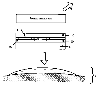
the surface relief pattern
not covered by the reflective material. This aforementioned patent application
provides an
optical structure having a light transmissive substrate having a surface
relief pattern formed
thereon; a patterned layer of a reflective material applied onto portions of
the surface relief
pattern of the light transmissive substrate, such that some portions of the
surface relief pattern
are covered by the reflective material, and other portions of the surface
relief pattern are
exposed. The structure further has an optically active coating underlying the
patterned layer
and exposed portions of the surface relief pattern. This structure is a type
of chromagram.
[0007] Another chromagram-type structure is described in United States
Patent application
20050128543 in the name of Phillips et al. In this publication patterned
substrates having
windowed regions that one can see through, are coated with optically variable
coatings or
optically variable inks that can be seen through the windows. For all intents
and purposes, all
references described heretofore or hereafter are incorporated herein by
reference.
[0008] Optically variable (OV) coating is understood as a coating providing
optically
variable effects, for example an observable color shift as the angle of
incident light or viewing
2
F "
CA 02587039 2007-05-02
Doc. No. 18-245 CA
Patent
angle changes. For example, the optical coating can be a multilayer optical
interference film
such as a three layer optical stack of absorber-dielectric-reflector, or
alternating layers of low
and high index of refraction dielectric layers. In addition, the optical
coating can be formed
from a plurality of multilayer optical interference flakes dispersed in a
polymeric medium such
as a color shifting ink. Another example of an OV coating is a tinted medium
with reflective
flakes dispersed therein. However this type of coating is not color shifting.
Its variable effects
appear as light and darker colors of the color of the tinted medium.
[0009] The aforementioned chromagrams combine security features of a
hologram and an
optically variable coating for enhanced protection. However, advanced security
features
increase the complexity and cost of protected objects. Accordingly, it is
desired to provide a
simple and cost effective method of protecting an object with a security
label, simpler and less
expensive than application of conventional chromagrams, while providing the
same advanced
security features.
[0010] Security devices providing holographic and OV effects, including
Chromagrams,
can be divided in two groups by a method of manufacturing. One group
encompasses devices
formed by covering a holographic structure by an OV coating, for example, a
thin-film stack or
a color shifting flakes in a polymeric coating. Devices of the second group
have a first
substrate with a hologram formed therein or thereon, adhesively bound,
preferably by hot
stamping, to a second substrate having an OV coating formed thereon.
[0011] The field of hot stamping and more particularly, hot stamping of one
optical coating
or substrate with another is well known. For example, coated substrates
bearing images, logos
or other indicia are hot stamped onto lottery cards, passports, banknotes,
driver's licenses, poker
chips, and a variety of other articles and substrates are well known.
[0012] Hot stamping is described or mentioned in the United States patents
5,002,312, US
5,059,245, US 5,135,812, US 5,171,363, US 5,186,787, US 5,279,657 and 7005178,
in the
name of Phillips et al. One commercially available machine for hot stamping
images onto
substrates is the Malahide E4-PK produced by Malahide Design and Manufacturing
Inc.
3
' "''r
CA 02587039 2007-05-02
Doc. No. 18-245 CA
Patent
Machines of this type are shown and described on the Internet at
www.hotstamping.com.
Simplistically, in a hot-stamping process, a die is attached to the heated
plate which is pressed
against a load roll of hot stamping foil to affix the foil to an article or
substrate.
[0013] Devices of both groups are disclosed for example in W00153113
application by
Phillips et al. and US Patent No. 7,054,042 to Holmes et al.
[0014] W00153113 discloses various security articles formed by laminating
laser imaged
optical coating structures to embossed substrates, wherein the laminated
articles include either
a color shifting foil or ink, which can be used as the background underneath a
holographic
image. '042 discloses optically decoupled devices comprising a relief
structure laminated with
an optically clear adhesive to a prefabricated thin film reflective structure
consisting of a
reflective layer, one or more dielectric layers, and a semi-transparent metal
layer.
[0015] Conventionally, when a security device of either type is used to
protect a valuable
object such as a document, a banknote, or any other object, the device is
adhesively coupled to
the object by an external adhesive layer. Therefore, devices of the second
group have two
adhesive layers: an internal adhesive layer for coupling the holographic
structure to the OV
structure and an external adhesive layer for coupling the resulting device to
the object.
[0016] It is an object of this invention to reduce a cost of protecting an
object by
eliminating one of the two adhesive layers and one of the two substrates,
while enabling the
same security features as provided by security devices of the second group. It
is an object of
the present invention to enable such security feature as an image having
combined holographic
and color shifting effects, by using a security label simpler than devices of
the first or second
types. ,It is also an object of the present invention to simplify the method
of protecting an
object by eliminating the step of applying an external adhesive layer and
forming a security
label on the surface of the object.
[0017] A security device from the second group, prefabricated by applying
an OV coating
onto a diffractive structure, such as a hologram, and then adhesively bonded
to an object, has
4
I I I d 141
CA 02587039 2007-05-02
Doc. No. 18-245 CA
Patent
the OV coating only in the area of the hologram. However, an additional
security feature can
be provided by an OV ink pattern on the surface of the object, e.g. a
banknote, extending
beyond the boundaries of the hologram label so that the ink design runs from
one part of the
banknote to the other. For example, an image of a duck is printed on the
banknote in color
shifting ink, but only its head is holographic in appearance. The head is
where the hologram is
stamped. This arrangement would be difficult to make using a prefabricated
hologram covered
with OV ink; it would require application of OV ink in two steps ¨ to the
hologram and to the
object, and a precise registration of these two images. It is an object of the
present invention to
provide a method for forming a security label on an object, wherein an OV
pattern extends
beyond the diffractive image formed by the label. It is further an object of
the present
invention to provide a method of manufacturing an object with a security label
formed thereon,
wherein an OV pattern on the object and an OV background of the security label
are formed in
one step.
[0018] Possible security breaches related to labels manufactured separately
and attached to
objects, are associated with transferring a label from a genuine document to a
counterfeit one,
or attaching wrongfully obtained security labels to counterfeit products. Such
problems can be
eliminated by using security substrates, wherein special optical effects are
provided by
substrates of the objects themselves and not by attached labels. An example of
security
substrates can be found in US Pat. No. 6,686,027 in the name of Caporaletti et
al. disclosing a
plastic substrate with build in color shifting security threads.
[0019] While providing a higher level of anti-counterfeit protection,
substrates like
disclosed in US Pat. No. 6,686,027 have significantly higher manufacturing
cost than small
security labels, in particular, because the whole object-size substrate has to
be processed in a
vacuum camera. The way of manufacturing such substrates imposes another
limitation, namely
on a material of the substrate, specified in US Pat. No. 6,686,027 as a
polymer.
[0020] It is an object of the present invention to provide a cost effective
security substrate
without limiting the material it is made of. In particular, it is an object of
the present invention
to provide a paper substrate for use in banknotes or paper documents.
" '11
CA 02587039 2007-05-02
Doc. No. 18-245 CA
Patent
[0021] It is known in the art that special inks printed onto paper
documents can be used as
security features. One particular type of special inks is an optically
variable (OV) ink
providing an optical effect dependent on a viewing angle. For example, US Pat.
No. 7,029,525
to Mehta teaches printing a paper document with water based color shifting
ink.
[0022] While application of OV ink is convenient and not expensive, by
itself it provides
only a moderate level of security. Accordingly, the present invention combines
security
features provided by the OV ink and a diffractive structure.
[0023] In addition, by printing OV ink directly onto the banknote, the ink
is forced into the
banknote fibers and thus the banknote becomes more secure as ink penetration
can be observed
by analytical methods. Such penetration would not occur with a prefabricated
hologram with
OV ink since a hot stamp adhesive would be between the banknote fibers and the
OV coating.
Another object of this invention is to allow two separate security features to
be made in
separate locations and then joined together where the product to be secured is
made. This
provides additional security since a prefabricated security label, such as a
hologram with an OV
coating, could be seized in transit, thus compromising the article to be
protected.
[0024] Various types of diffractive structures can be used while forming a
security label
according to the present invention. A patterned by demetallization hologram or
a windowed
hologram together with a color shifting coating allow for light impinged onto
the hologram to
reach the color shifting coating underneath thus enabling a synergy of
diffractive and color
shifting optical effects.
[0025] A patterned layer of a reflective material may be applied over
predetermined
portions of the holographic substrate to form alphanumeric characters, bar
codes, pictorial or
graphic designs. A highly reflective material, such as aluminum, is deposited
on the surface of
the holographic substrate and etched out off predetermined portions of the
substrate. As a
result of demetallizing, the areas of the substrate where the metal was etched
out become
essential Ey transparent and the holographic effect there becomes almost
invisible. In contrast,
6
CA 02587039 2007-05-02
Doc. No. 18-245 CA
Patent
the portions of the substrate where the reflective metal was left on the
surface in different
predetermined shapes, maintain visible holographic properties.
[0026] It is another object of this invention to provide a synergy of
diffractive and OV
effects by using a demetallized or windowed hologram optically coupled by an
adhesive layer
to an OV coating underneath.
SUMMARY OF THE INVENTION
[0027] In accordance with one aspect of this invention, a method of forming
a label on an
object is provided, comprising a step of coating a surface of the object with
optically variable
ink, and characterized by comprising a step of bonding a patterned structure
to the object with a
light transmissive adhesive over the optically variable ink, wherein the
patterned structure
allows light to propagate therethrough, whereby the label, when irradiated
with light, forms an
image having an optically variable background.
[0028] In accordance with another aspect of this invention, a patterned
structure to be
utilized by the method of the present invention is provided, which is a
diffractive structure
comprising one of: a semi transparent reflective layer, a high refraction
index layer, and a
patterned reflective coating, whereby the image formed by the label has a
holographic effect
provided by the diffractive structure and an optically variable effect
provided by the optically
variable ink.
[0029] In accordance with yet another aspect of this invention, an article
is provided
comprising: a substrate, a coating of optically variable ink applied onto the
substrate, a
diffractive structure adhesively bonded to the substrate over the coating of
optically variable
ink, and an adhesive layer for bonding the diffractive structure to the
substrate. The article is
characterized in that the diffractive structure comprises a reflective layer
such that, when the
article is irradiated with light, a first portion of light is reflected by the
reflective layer and a
second portion of light propagates through the reflective layer to the coating
of optically
variable ink, and the first and second portions of the light after being
reflected by the reflective
7
CA 02587039 2007-05-02
Doc. No. 18-245 CA
Patent
layer and the coating of optically variable ink, respectively, form a specular
image having an
optically variable feature.
[0030] In an embodiment of this invention, optically variable ink is first
printed on a
banknote of a paper document followed by hot-stamp process bonding together
the optically
variable ink layer with a substrate having a windowed hologram.
[0031] In an aspect of the invention, the optically variable ink can be
seen through portions
of the demetallized hologram or both can be seen at the same time.
[0032] In accordance with the invention, an optical structure is provided
wherein a
demetallized hologram is hot stamped on to an optically variable foil.
BRIEF DESCRIPTION OF THE DRAWINGS
[0033] To further clarify the above and other advantages and features of
the present
invention, a more particular description of the invention will be rendered by
reference to
specific embodiments thereof that are illustrated in the appended drawings. It
is to be
appreciated that these drawings depict only typical embodiments of the
invention and are
therefore not to be considered limiting of its scope. The invention will be
described and
explained with additional specificity and detail through the use of the
accompanying drawings
in which:
[0034] Fig. 1 is a cross-sectional view of a Chromagram formed in
accordance with one
embodiment of the present invention.
[0035] Fig. 2 is a cross sectional view of a patterned structure in the
chromagram shown in
Fig. 1.
[0036] Fig. 3 is a cross-sectional view of a Chromagram formed on a
banknote.
8
"i
CA 02587039 2007-05-02
Doc. No. 18-245 CA
Patent
[0037] Fig. 4 is a cross-sectional view of a Chromagram, wherein the
adhesive contains
covert flakes or a low concentration of optically variable flakes or optically
variable magnetic
flakes.
[0038] Fig. 5 is a cross-sectional view of a Chromagram wherein a grating
is supported by,
or formed therein, a layer of high refraction index material.
[0039] Fig. 6 is a cross-sectional view of a Chromagram wherein a demet
hologram is
supported by a layer of high refraction index material.
[0040] Fig. 7 is a schematic depiction of forming the Chromagram shown in
Fig. 6.
DETAILED DESCRIPTION
[0041] According to the present invention, a security label, or chromagram,
is formed on a
surface of an object by printing optically variable ink onto the surface and
then adhesively
bonding a patterned structure thereon.
[0042] The optically variable ink comprises a carrier medium with OV flakes
dispersed
therein. It should be appreciated that carrier media can be of various types.
For example, a
water-based OV ink is disclosed in US Pat. No. 7,029,525 in the name of Mehta,
and a
polymer-based OV ink is taught in US Pat. No. 5,279,657 in the name of
Phillips et al. By way
of example, the carrier of the OV ink is acrylic- or urethane-based ink. It
should be understood
that a thicker carrier with OV flakes therein, also called OV paint, is
considered to be a type of
the OV ink for the purpose of this application. In some embodiments, the
carrier is tinted and/or
contains magnetic particles.
[0043] The OV flakes can be color shifting flakes such as disclosed in US
Pat. No.
6,751,022 in the name of Phillips and US Patent No. 6,749,777 in the name of
Argoitia et al.,
reflective flakes, magnetic reflective or magnetic color shifting flakes such
as disclosed in US
6,818,299 to Phillips and in US 6,586,098 to Coulter et al.
9
I "
CA 02587039 2007-05-02
Doc. No. 18-245 CA
Patent
[0044] The reflective flakes are preferably used in a tinted medium for
some applications.
Both, the color shifting and reflective flakes provide optical effects that
vary with viewing
angle.
[0045] The optically variable ink can be utilized in various printing
processes, such as
lithographic printing, flexographic printing, letterpress printing, intaglio
printing, gravure
printing, screen printing, ink jet printing, and by electrostatic printing.
[0046] According to the teachings of the present invention, the OV ink is
applied directly
onto the object, which means that the surface of the object can be covered
with ink, paint, or
lacquer, which is understood to be a portion of the object. "Applied directly
onto the object"
has a meaning opposite to applying OV ink onto a substrate separate from the
object and then
bonding this ink-covered substrate to the object. "Applied directly" means
that no other
substrates are disposed between the OV coating and the substrate of the object
to be protected
or decorated by the method of the present invention.
[0047] The method of the present invention allows forming a security label
on a wide
variety of objects, including large size objects and objects made of paper,
plastic, metal, etc.
This is a significant departure from the aforedescribed conventional method of
forming a
security label on a polymeric substrate and then bonding the label to an
object.
[0048] According to the present invention, a security label is formed on a
surface of an
object by adhesively bonding a patterned structure to the coating of OV ink
with an adhesive,
which may be an energy activated adhesive.
[0049] For the purpose of this application, the term "energy activated
adhesive" means a
bonding substance that requires an energy source for curing. The energy
activated adhesives
include, but are not limited to, hot stamp adhesives, UV or e-beam activated
adhesives,
thermoplastic and thermoset adhesives, paint¨based polymeric compositions,
varnishes, and
staining compositions. By way of example, an adhesive is selected from the
group of:
i
.1.
CA 02587039 2007-05-02
Doc. No. 18-245 CA
Patent
polymethacrylate, polyacrylate, polyamide, nitrocellulose, alkyd resin,
polyvinyl alcohol,
polyvinyl acetate, and polyurethane.
[0050] The methods of activating the adhesives include hot stamping, UV
curing, applying
heat, pressure, or a beam of electrons. For brevity, an energy activated
adhesive, possibly with
special particles therein, is referred to as "an adhesive" hereinbelow.
[0051] The adhesive may be printed into patterns or flood coated over the
entire surface. If
patterned, the product becomes more tamper proof since the product can not be
physically
removed in one piece. Attempts to remove the device by dissolving the adhesive
using solvents
would also be detrimental since the solvent would also attack the
hardcoat/release which in turn
would destroy the device, making tampering obvious.
[0052] Preferably, the adhesive is applied to the patterned structure,
however in different
embodiments of the present invention the adhesive can be applied and cured
upon either a
patterned structure or over the OV ink, or both, prior to bonding the two
surfaces together.
[0053] The method disclosed in the present application makes use of a
patterned structure,
which in one embodiment of the present invention consists of a patterned
coating on a
substrate, wherein the substrate is optionally removable in the process of
forming a security
label on a surface of an object printed with OV ink.
[0054] In other embodiments the patterned structure can take various
conventional forms of
a diffractive structure, including diffraction patterns such as diffraction
gratings, refraction
patterns, holographic patterns such as two-dimensional and three-dimensional
holographic
images, &metallized holograms, coatings with varied index of refraction, light
transmissive
dielectric coatings with refractive flakes therein or thereon, KinegramR
devices, PixelgramR
devices, corner cube reflectors, zero order diffraction structures, moire
patterns, and light
interference patterns based on microstructures having dimensions of from about
0.11AM to
about 10 1.irri.
11
I I I Iµ
CA 02587039 2007-05-02
Doc. No. 18-245 CA
Patent
[0055] In one embodiment of the present invention, the diffractive
structure is embossed on
an embossable resin layer made of such materials as, polyvinyl chloride or
polymethacrylate.
The embossable layer may also provide functionality of a hardcoat/release
layer. The
embossing may be either patterned or continuous.
[0056] In another embodiment of the present invention, the diffractive
structure comprises
a grating formed in a substrate, preferably a light transmissive or
essentially transparent
substrate, which may be made of type G PET, Polycarbonate Oriented
Polypropylene (OPF'),
Polyvinyl Chloride or other suitable plastic material. By way of example, a
PET layer has a
thickness of 6-25 microns.
[0057] Alternatively, the patterned structure comprises a holographic
pattern formed by
embossed metal particles or optical stack flakes, as disclosed in Patent Nos.
5,624,076 and
5,672,410 to Miekka et al. Alternatively, the embossed particles can be metal-
dielectric
pigments.
[0058] Optionally, for improved visibility of holographic effects, the
aforementioned
structures have some form of reflective material underneath, either a highly
reflective metal
like Al, or other metals, or a high index layer made of ZnS, Ti02, or Zr02.
[0059] A security label formed on the surface of an object is designed to
be viewed from
the side of a patterned structure, thus for the OV effect provided by the
underlining OV coating
to be visible, the patterned structure has to have light transmissive regions.
[0060] In one embodiment of the present invention, the diffractive
structure comprises a
patterned opaque layer having one or more light transmissive regions, or
windows, to allow
optical effects provided by the optically variable coating be visible through
said windows when
the device is viewed from the side of the diffractive structure. Preferably,
the windowed
coating is reflective to provide a highly reflective holographic image with an
optically variable
background.
12
CA 02587039 2007-05-02
Doc. No. 18-245 CA
Patent
[0061] The reflective layer underneath the diffractive structure can be
patterned by
demetallization, as it is known to one skilled in the art. A demetallized
layer can be made of
Al, Cu, Ni, and other metals and metal alloys that have been patterned by
demetallization.
Various techniques may be used to pattern the metal layer, such as chemical
etching or oil
ablation in vacuum, preferably, both done in registration with the relief
image.
[0062] The method of demetallization allows making intricate, lace-like
patterns as well as
patterns with relatively wide windows. While lace-like patterns are more
difficult to reproduce,
for example by a metallic pen, windows of larger size, by way of example at
least lmm wide
and preferably at least 5 mm wide, to allow more of the OV background to be
visible.
[0063] In one embodiment of the present invention, shown in Fig. 1, a
patterned structure
used for forming a security label is a diffractive structure with a windowed
reflective layer.
The structure shown in Fig. 1 is a result of adhesively joining the
diffractive structure to an
object 24 with adhesive layer 62. The object 24 has an OV coating of carrier
34 with OV
flakes 35 suspended within the carrier 34, applied onto the surface of object
64. The diffractive
structure is formed on substrate 12, which can be a resin/hardcoat layer and
has grating 14
thereon partially coated with a pattern of highly reflective coating 16 in
contact with portions of
grating 14, for preventing light from passing therethrough. Resin layer 12 is
optionally covered
with protective light transmissive layer 28 with opaque indicia 19 printed
thereon. Preferably,
grating 14 is embossed onto substrate 12 and covered with patterned
demetallized aluminum
16, and then the demet hologram is hot stamped or hot roll nipped to the
object 24 using clear
hot stamp adhesive 62. The uncoated portions of the hologram are substantially
light
transmissive.
[0064] Preferably, reflective layer 16 is windowed, so that substrate 12
has one or more
regions 100 thereon, embossed and covered with reflective material, said
regions separated by
regions 17 shown in Fig. 2, not covered with aluminum and can be either
embossed or not-
embossed.
[0065] When the structure shown in Fig. 1 is viewed from the top, it
provides a highly-
13
CA 02587039 2007-05-02
Doc. No. 18-245 CA
Patent
reflective holographic image having windows wherein a color shifting
background shows. The
combined optical effect is enhanced by printed indicia.
[0066] It is preferable to pattern reflective layer 16, because it is
easier to emboss the whole
region, then pattern the reflective layer, and then apply the optically
matching adhesive.
Alternatively, the continuous reflective coating is shifted to one side; the
resulting structure has
planar reflective coating over non-embossed regions, providing highly
reflective mirror-like
portions of the image as an additional optical effect.
[0067] With reference to Fig. 3, in another embodiment of the present
invention, object or
substrate 68 is a banknote or any other type security document. A security
structure is formed
by printing a color shift ink onto banknote 68 as a background color, and then
hot stamping a
demet hologram, preferably embossed onto resin/hardcoat layer 12 and supported
by carrier
sheet 66, over the ink using transparent hot stamp adhesive 62.
[0068] Optionally, adhesive 62 contains other particles or flakes to modify
the color of the
color shift ink or as a covert security feature. By way of example, adhesive
62 may contain
fluorescent materials, covert charms, such as disclosed in U.S. Patent
Application
20050037192 by Argoitia et al, upshift phosphors, interference pigments like
mica-based
interference flakes, and non-shifting pigments or dyes. The covert flakes are
detectable under a
microscope, whereas for the fluorescent and phosphor materials, irradiation of
the device by
UV or IR. light is required to activate those features. Since resin/hardcoat
layer 12 is quite thin,
preferably less than 3 microns, the UV or IR light is able to penetrate to the
particles in
adhesive 62. In Fig. 3, a release layer, resin layer and hard coat are shown
as one layer 12
providing functionality of each of the three layers. In other embodiments,
layer 12 is replaced
by any combination of separate layers: a resin layer for embossing, a release
layer for releasing
the demet hologram from carrier sheet 66, and a hard coat layer for durability
of the transferred
device.
[0069] In another embodiment of the present invention shown in Fig. 4,
covert flakes 45
that cannot be seen with the unaided eye are mixed into hot stamp adhesive 40
used to bond the
14
CA 02587039 2014-04-03
Doc. No. 18-245 CA
Patent
two structures together as in the previous embodiments. The examples of covert
flakes include,
but not limited to, charms or taggants as taught in United States patent
application publication
number 2006/0035080 incorporated herein by reference, shaped pigments as
disclosed in United
States patent application publication number 20060035080, magnetic flakes,
fluorescent
pigments, standard UV activated to form visible light, or specialized anti-
Stokes materials UV
activated, to form visible light.
[0070] These covert flakes serve as a means of authentication. If the covert
flakes provide an
optical effect, for example under a microscope or being IR activated,
additionally to holographic
effects exhibited by this structure, though the windows where the Al coating
is missing, covert
flakes 45 can be seen on color shifting background. In another embodiment,
optically variable
flakes are added to adhesive 40 at low concentrations so that the OV foil
colors are modified
when viewing from the top.
[0071] The structure shown in Fig. 4, when viewed from the top, provides a
highly- reflective
holographic image formed by pattern 14, and a color-shifting background
visible in the windows.
Covert flakes 45 are visible in UV or IR light, or under a microscope. The
cover flakes appear
within the windows on the color shifting background. If substrate 64 is
transparent or light
transmissive, then, through substrate 64, one can see a color shift with a
faint reflection hologram
where aluminum 16 is present and indicia 19 where aluminum 16 is absent.
[0072] In one embodiment of the present invention, shown in Fig. 5, the
diffractive structure
comprises a light transmissive hologram, formed by relief pattern 14 embossed
in light
transmissive hardcoat/resin layer 70, and a high refraction index layer 50
disposed between
adhesive layer 62 and embossed relief pattern 14 for preventing index matching
between
adhesive 62 and resin 70. The high refraction index layer 50 is made of a
material having an
index of refraction no less than 1.65, by way of example, the high refractive
index layer can be
made of ZnS, Ti02, Zr02, etc.
[0073] When forming a security label, the diffractive structure made of resin
layer 70 with
CA 02587039 2007-05-02
Doc. No. 18-245 CA
Patent
relief 14, covered with high index coating 50 and adhesive 62, is coupled to
an object 24
having a coating of OV ink, for example color shifting ink. Optionally, the
diffractive structure
can be formed on a removable substrate, or resin/hardcoat layer 70 can serve
as a substrate for
the diffractive structure. Preferably, the diffractive structure is coupled to
the object by hot
stamping, and adhesive 62 is a dry hot stamp adhesive.
[0074] In operation, when the security label formed in accordance with this
embodiment is
irradiated with light, one portion of light reflects at the surface dividing
resin layer 70 and high
index layer 50, and forms a holographic non-OV image. Another portion of light
propagates
through high index layer 50 and adhesive 62 to the OV coating and reflects
back to a top
surface of resin layer 70 carrying a color-shifting effect from the OV coating
as well as a
holographic image. Thus, the security label provides a color shifting
holographic image by
combining the effects of the optically variable and diffractive structures,
wherein a visual effect
is produced by an interaction between light reflecting from the optically
variable ink and light
diffracted from the diffractive structure.
[0075] In another embodiment of the present invention, the diffractive
structure comprises
a semitransparent reflective layer replacing high-index layer 50 in Fig. 5.
Optical effects
provided by this embodiment are very similar to the aforedescribed effects of
the embodiment
shown in Fig. 5 and comprising a high-index layer.
[0076] In another embodiment of the present invention shown in Fig. 6, a
diffractive
structure includes grating 14 supported by, or formed therein, hardcoat/resin
layer 70, patterned
reflective layer 16, and a layer of high refraction index material 50. A
security label is formed
by hot stamping this diffractive structure over an object 24 covered with OV
ink. The process
of forming such security label on a surface of an object, for example a
printed banknote, is
schematically shown in Fig. 7.
[0077] When viewed from the top, as shown in Fig. 6, this structure
provides an image with
a combination of optical effects. One part of the image is a specular
holographic image formed
by light reflected from opaque metallic layer 16. This part of the image is
complemented by a
16
CA 02587039 2007-05-02
Doc. No. 18-245 CA
Patent
color shifting specular holographic image formed by light reflecting from the
regions where
reflective layer 16 has windows, so that the corresponding portion of the
image is produced by
an interaction between light reflecting from the optically variable ink and
light diffracted from
the diffractive structure having a high index layer and exhibits optical
effects provided by both,
the diffractive structure and the OV coating.
[0078] In a structure similar to the structure shown in Fig. 6 but without
a high refraction
index coating, regions wherein reflective layer 16 has windows, show very weak
holographic
effects or no holographic effects. If the adhesive 62 has a complete index
match to the resin
layer 70, then no holographic effects will be seen. This is very much
dependent upon the degree
of index matching between the coating underlying the non-aluminized portion of
the hologram
and the adhesive. If there is a refractive index differential of at least 0.2
for the real part of the
refractive index, then some holographic effects will be seen. The greater the
refractive index
differential, the more clearly the hologram will be seen. By way of example, a
refractive index
differential of 0.8, between a substrate with n=1.5 and a high index coating
with n=2.3,
provides brightness of a transparent hologram.
[0079] In reference to Figs. 5 and 6, high refraction index coating 50 has
an index of
refraction no less than 1.65. Suitable examples of such a high index
transparent layer include
TiO<sub>2</sub> or ZnS.
[0080] In the aforedescribed embodiments wherein a diffractive structure
comprises a semi
transparent reflective layer or a high refraction index layer, the holographic
image formed by
the label is at least in part a color shifting holographic image. The color
shifting part of the
holographic image is formed by interaction of light diffracted by the
diffractive structure and
light reflected by the OV coating, whereby this part of the image exhibits a
synergy of
holographic and optically variable effects. The colors resulting from the
interaction of
diffractive light and thin film interference light may add or subtract to the
diffractive colors
resulting in a unique optical spectrum as a function of viewing angle.
[0081] In another embodiment of the present invention, alternatively to hot-
stamping, a UV
17
CA 02587039 2007-05-02
Doc. No. 18-245 CA
Patent
activated adhesive is used to bond the two structures together. By way of
example, an object or
substrate printed with color shifting ink and with an adhesive over the ink,
is brought together
with a laminating sheet containing the demet hologram; the adhesive is then
cured by
irradiating the laminating sheet with UV light or electron beam, wherein the
laminating sheet
has a transparent or at least UV-transmissive substrate. One way to overcome
the obstacle to
UV light posed by the reflective metal covering the hologram, is to use a
patterned or
windowed reflective layer wherein areas covered with metal are very narrow,
estimated to be
less than 2 microns, so that UV light can cure the adhesive by coming in at an
angle. Another
way is to use e-beam curing. Alternatively, semitransparent reflective layer
or a high index
layer will allow some UV light through to the adhesive layer.
[0082] In one embodiment of the present invention, adhesive layer is
patterned so that the
patterned structure has regions not bonded to the optically variable coating
on the object or
substrate.
[0083] In another embodiment of the present invention, adhesive and OV ink
are printed
onto different regions on the surface of the object, and a patterned structure
is bonded to the
object with the adhesive forming a frame, or a part of it, around the OV
coating.
[0084] In one embodiment of the present invention, an article is formed by
covering a light
transmissive substrate with OV ink and then adhesively bonding, preferably by
hot-stamping,
to a diffractive structure, wherein the diffractive structure is a hologram
underlined with a
reflective layer such that both reflects light and allows light therethrough
to provide optical
coupling between the OV coating and the hologram. Preferably, the OV ink is a
color shifting
ink printed onto the substrate, the bonding method is hot stamping, and the
reflective layer is
aluminum patterned by demetallization. Alternatively, the reflective layer is
a semitransparent
metal layer, or a high index dielectric coating. The substrate is either
opaque or light
transmissive.
[0085] A light transmissive substrate, preferably made of PET, provides for
viewing the
device from both sides, which is advantageous if the optically variable
coating is light
18
,
10,4,
CA 02587039 2007-05-02
Doc. No. 18-245 CA
Patent
transmissive, i.e. formed by a light transmissive OV ink, for example having a
low density of
optically variable flakes incorporating opaque Fabry Perot filters, or one
based on all dielectric
transparent optically variable flakes, or an ink comprising absorber-spacer-
absorber flakes
disclosed in U.S. Pat. No. 5,278,590 in the name of Phillips et al. When this
construction is
viewed through the OV ink covered substrate, a superposition of the
holographic and optically
variable effects is visible, i.e. one can see a color shift with a faint
reflection hologram where
aluminum is present. In essence, the rainbow of colors that were in the
initial hologram has
been modified by the OV structure, whereby some colors are accentuated and
some are
suppressed. When this structure is viewed from the side of the diffractive
structure, one can see
a highly-reflective holographic image with a color-shifting background visible
in windows of
the reflective layer covering the hologram. This construction is particularly
adapted to
banknotes employing transparent plastic substrates where both sides can be
viewed.
[0086] In another embodiment of the present invention, an optically
variable foil
comprising OV ink coating is hot stamped, or adhesively bonded by another
method, to a
demetallized hologram. Alternatively, the hologram can be coated with
semitransparent
reflective layer, patterned or non-patterned, or a coating of a high index
material, as it was
described before.
19