Note : Les descriptions sont présentées dans la langue officielle dans laquelle elles ont été soumises.
CA 02587150 2010-06-30
77496-245
COMBINATION EAS AND RFID LABEL OR TAG
BACKGROUND
1. Technical Field
[0002] The present disclosure relates to an electronic article surveillance
(EAS)
label or tag for the prevention or deterrence of unauthorized removal of
articles from a
controlled area. More particularly, the present disclosure relates to an EAS
label or
tag combined with a radiofrequency identification (RFID) label or tag for
recordation
of data specific to the article and a novel RFID label or tag.
2. Description of Related Art
[0003] Electronic article surveillance (EAS) systems are generally known in
the
art for the prevention or deterrence of unauthorized removal of articles from
a
controlled area. In a typical EAS system, EAS markers (tags or labels) are
designed
to interact with an electromagnetic field located at the exits of the
controlled area,
such as a retail store. These EAS markers are attached to the articles to be
protected.
If an EAS tag is brought into the electromagnetic field or "interrogation
zone," the
presence of the tag is detected and appropriate action is taken, such as
generating an
alarm. For authorized removal of the article, the EAS tag can be deactivated,
removed or passed around the electromagnetic field to prevent detection by the
EAS
system.
[0004] EAS systems typically employ either reusable EAS tags or disposable EAS
tags or labels to monitor articles to prevent shoplifting and unauthorized
removal of
articles from the store. The reusable EAS tags are normally removed from the
articles
before the customer exits the store. The disposable tags or labels are
generally
attached to the packaging by adhesive or are located inside the packaging.
These tags
typically remain with the articles and must be deactivated before they are
removed
from the store by the customer. Deactivation devices may use coils which are
1
CA 02587150 2010-06-30
77496-245
energized to generate a magnetic field of sufficient magnitude to render the
EAS tag
inactive. The deactivated tags are no longer responsive to the incident energy
of the
EAS system so that an alarm is not triggered.
[0005] For situations where an article having an EAS tag is to be checked-in
or
returned to the controlled area, the EAS tag must be activated or re-attached
to once
again provide theft deterrence. Because of the desirability of source tagging,
in which
EAS tags are applied to articles at the point of manufacturing or
distribution, it is
typically preferable that the EAS tags be deactivatable and activatable rather
than be
removed from the articles. In addition, passing the article around the
interrogation
zone presents other problems because the EAS tag remains active and can
interact
with EAS systems in other controlled areas inadvertently activating those
systems.
[0006] Radio-frequency identification (RFID) systems are also generally known
in the art and may be used for a number of applications, such as managing
inventory,
electronic access control, security systems, and automatic identification of
cars on toll
roads. An RFID system typically includes an RFID reader and an RFID device.
The
RFID reader may transmit a radio-frequency carrier signal to the RFID device.
The
RFID device may respond to the carrier signal with a data signal encoded with
information stored by the REID device.
[0007] The market need for combining EAS and RFID functions in the retail
environment is rapidly emerging. Many retail stores that now have EAS for
shoplifting protection rely on bar code information for inventory control.
RFID offers
faster and more detailed inventory control over the bar code. Retail stores
already pay
a considerable amount for hard tags that are re-useable. Adding RFID
technology to
EAS hard tags could easily pay for the added cost due to improved productivity
in
inventory control as well as loss prevention.
2
CA 02587150 2010-06-30
77496-245
SUMMARY
[0008] It is an object of some embodiments of the present disclosure to
provide a tag or label which in one tag or label combines the features of an
independent EAS tag or label and an independent RFID tag or label.
According to an aspect of the present invention, there is provided a
security tag comprising: an electronic article surveillance (EAS) component
having
a defined surface area; and a radio frequency (RFID) component, the RFID
component comprising: an antenna configured to impedance match using
properties of the EAS component; and a defined surface area, the defined
surface
area of the EAS component being configured to at least partially overlap the
defined surface area of the RFID component.
According to another aspect of the present invention, there is
provided a security tag comprising: an electronic article surveillance (EAS)
component having a defined surface area; and radio frequency identification
(RFID) component having: an antenna configured to impedance match using
properties of the EAS component; a defined surface area, the surface area of
the
EAS component configured to at least partially overlap the surface area of the
RFID component; and an application specific integrated circuit (ASIC), the
ASIC
having a complex impedance, the complex impedance of the ASIC being
configured to match a coupled complex conjugate impedance of the antenna and
the EAS component.
According to another aspect of the present invention, there is
provided a method of operating a combination of an electronic article
surveillance
(EAS) component and a radio frequency identification (RFID) component, the
method comprising the step of: arranging the RFID component to overlap with
the
EAS component; and using the EAS component to adjust an impedance of an
antenna associated with the RFID component.
[0009] The present disclosure relates to a security tag which includes an
EAS component having a defined surface area, and an RFID component having a
defined surface area. The defined surface area of the EAS component is
2a
CA 02587150 2010-06-30
77496-245
configured to at least partially overlap the defined surface area of the RFID
component.
[0010] The RFID component includes an antenna and the antenna may at least
partially overlap the defined surface area of the EAS component- A
substantially
planar spacer having a thickness may be at least partially disposed between
the
defined surface area of the EAS component and the defined surface area of the
RFID
component. The thickness of the spacer determines a read range between an RFID
reader and the RFID component, and the RFID reader is capable of activating
the
RFID component when the RFID component is within the read range. The antenna
and the HAS component may form a part of an impedance matching network of the
antenna. The antenna impedance may include loading effects of the EAS
component.
The RFID component may include the antenna and an application specific
integrated
circuit (ASIC). The ASIC may have a complex impedance. The complex impedance
of the ASIC may match a coupled complex conjugate impedance of the antenna
including the loading effects of the EAS component. A material for a base
portion of
the RFID component may be selected from the group consisting of (a) base
paper, (b)
polyethylene, (c) polyester; (d) polyethyleneterephthalate (PET); and (e)
polyetherimide (PEI). The base portion material may be plastic having a
dielectric
constant of about 3.3 and a loss tangent of less than about 0.01. The spacer
material
may be selected from the group consisting of (a) a low loss, low dielectric
material;
and (b) air.
[0011] The present invention relates also to a method of operating a
combination
of an electronic article surveillance _(EAS) component and a radiofrequency
identification (RFID) component In some embodiments, the method includes the
step of moving
the RFID component to be overlapped by the EAS component so as to change the
impedance of
an antenna coupled to the RFID component. The impedance of the antenna
includes
the loading effects of the EAS component The antenna may include an antenna
conductor and the antenna is tuned by severing the antenna conductor into at
least two
segments such that at least one segment point corresponds to an operating
frequency
for the antenna based upon the length of the at least two antenna segments,
and
isolating the severed antenna conductor from remaining portions of the
conductor.
[0012] The method may further include the combination of an electronic article
surveillance (EAS) component and a radiofrequency identification (RFID)
component
3
CA 02587150 2007-05-09
WO 2006/055653 PCT/US2005/041573
having a spacer disposed therebetween, with the spacer having a thickness, and
the
method may include the step of varying the thickness of the spacer. The step
of
varying the thickness of the spacer may vary a read range between an RFID
reader
and the RFID component, and wherein the RFID reader is capable of activating
the
RFID component when the RFID component is within the read range.
BRIEF DESCRIPTION OF THE DRAWINGS
[0013] The subject matter regarded as the embodiments is particularly pointed
out
and distinctly claimed in the concluding portion of the specification. The
embodiments, however, both as to organization and method of operation,
together
with objects, features, and advantages thereof, may best be understood by
reference to
the following detailed description when read with the accompanying drawings in
which:
[0014] FIG. 1 illustrates a combination EAS/RFID security tag according to one
embodiment of the present disclosure;
[0015] FIG. 2A illustrates one part of sample testing data for a combination
EAS/RFID security tag according to one embodiment of the present disclosure;
[0016] FIG. 2B illustrates another part of sample testing data for a
combination
EAS/RFID security tag according to one embodiment of the present disclosure;
[0017] FIG. 3A illustrates an RFID system using magnetic field coupling in
accordance with one embodiment of the present disclosure;
[0018] FIG. 3B illustrates an RFID system using electric field coupling in
accordance with one embodiment of the present disclosure;
[0019] FIG. 4 illustrates a perspective exploded view of a security tag in
accordance with one embodiment of the present disclosure;
[0020] FIG. 5 illustrates a top view of the security tag of FIG. 4;
[0021] FIG. 6 illustrates a top view of a security tag with an antenna having
segment points in accordance with an alternate embodiment of the present
disclosure;
[0022] FIG. 7 illustrates a block flow diagram in accordance with one
embodiment of the present disclosure;
[0023] FIG. 8A illustrates a prior art configuration of a co-planar EAS label
adjacent to an RFID label;
4
CA 02587150 2010-06-30
77496-245
[0024] FIG. 8B illustrates a prior art configuration of a co-planar EAS label
and
an RFID label which are separated by a gap;
[0025] FIG. 8C illustrates an embodiment of the present disclosure of a
combination EAS component with an RFID component mounted directly underneath
the EAS component;
[0026] FIG. 8D illustrates an embodiment of the present disclosure of one
portion
of a security tag combination EAS component with an RFID component insert; .
[00271 FIG. 8E is an elevation view of the embodiment of the present
disclosure
of FIG. 8D;
[0028] FIG. 8F illustrates an embodiment of the present disclosure of one
portion
of a security tag combination EAS component with an RFID component insert; and
[0029] FIG. 8G is an elevation view of the embodiment of the present
disclosure
of FIG. 8F.
DETAILED DESCRIPTION
[0031] The present disclosure will be understood more fully from the detailed
description given below and from the accompanying drawings of particular
embodiments of the invention which, however, should not be taken to limit the
invention to a specific embodiment but are for explanatory purposes.
[0032] Numerous specific details may be set forth herein to provide a thorough
understanding of a number of possible embodiments of a combination EAS/RFID
tag
incorporating the.present disclosure. It will be understood by those skilled
in the art,
however, that the embodiments may be practiced without these specific details.
In
other instances, well-known methods, procedures, components and circuits have
not
been described in detail so as not to obscure the embodiments. It can be
appreciated
that the specific structural and functional details disclosed herein may be.
representative and do not necessarily limit the scope of the embodiments.
[0033] Some embodiments may be described using the expression "coupled" and
"connected" along with their derivatives. For example, some embodiments may be
5
CA 02587150 2007-05-09
WO 2006/055653 PCT/US2005/041573
described using the term "connected" to indicate that two or more elements are
in
direct physical or electrical contact with each other. In another example,
some
embodiments may be described using the term "coupled" to indicate that two or
more
elements are in direct physical or electrical contact. The term "coupled,"
however,
may also mean that two or more elements are not in direct contact with each
other, but
yet still co-operate or interact with each other. The embodiments disclosed
herein are
not necessarily limited in this context.
[0034] It is worthy to note that any reference in the specification to "one
embodiment" or "an embodiment' 'means that a particular feature, structure, or
characteristic described in connection with the embodiment is included in at
least one
embodiment. The appearances of the phrase "in one embodiment" in various
places
in the specification are not necessarily all referring to the same embodiment.
[0035] Turning now to the details of the present disclosure, one manner in
which
a combination EAS/RFID label (or tag) may be utilized is to put both the EAS
related
components together with the RFID related components and package them
together.
However, there may be some electrically or electro-mechanical interacting
factors that
may affect the performance of either the EAS function and/or the RFID
function.
Placing the RFID label on top of the EAS label is the most convenient way but
may
result in substantial de-tuning and signal loss for the RFID label. For
example, in a
typical RFID device, performance of the RFID label is typically very sensitive
to
impedance matching of an application specific integrated circuit (ASIC)/lead
frame
assembly for the RFID device to the effective impedance of an RFID antenna
mounted on a substrate. A more detailed description of some possible
embodiments
of the RFID portion of the device is discussed further below. Other objects
surrounding the RFID label may contribute to either the effective impedance or
the
absorption of electromagnetic energy used to read the RFID label.
[0036] Some existing 2450 MHz EAS/RFID combination labels have used a
configuration where an RFID label and an EAS label are placed in an overlapped
configuration. There may be considerable degradation in RFID label detection
with
this particular application. Although end-to-end or slight overlap has worked
best in
such systems, the tag size tends to become prohibitively large in these
instances.
Also, a side-by-side configuration has been known to create an irregular RFID
detection pattern. There are not many designs which have been able to
successfully
6
CA 02587150 2007-05-09
WO 2006/055653 PCT/US2005/041573
implement a combination EAS/RFID tag in the marketplace. Most applications
using
combined EAS and RFID of tagged items use separate EAS and RFID labels that
are
mounted separately so that they occupy considerable space on the tagged item
than
either one would occupy by itself if mounted separately.
[0037] It is envisioned that the solution to this problem is the use of an EAS
label
portion of the combination tag as part of the impedance matching network for
the
RFID label. For example, as the RFID label is placed closer and closer to the
EAS
label, the RFID label antenna impedance is affected, or tuned, by the EAS
label. In
order to achieve RFID label impedance matching, the REID antenna geometry may
itself be designed so that any resulting electrical effect of the EAS label on
the
impedance is taken into account. For example, the RFID antenna may be
configured
to have a highly capacitive impedance and which may be grossly mismatched to
the
impedance of the logic chip for the device (e.g., an ASIC/lead frame assembly
as
referred to above). As the RFID label is placed proximate the EAS label e.g.,
directly
underneath, the impedance of the RFID antenna is nearly matched to the ASIC
impedance.
[0038] FIG. 1 generally illustrates an EAS component 1 and an RFID component
2. The EAS component 1 is an EAS label or tag. EAS component 1 may contain,
for
example but is not limited to, a magnetic resonator element along with a bias
magnet
(or other EAS type resonant circuits) that is contained in a housing of
plastic or some
other material. Other EAS labels or tags not specifically disclosed herein may
perform the function of EAS component 1. The RFID component 2 is an RFID label
or tag. RFID component 2 may contain, for example and is not limited to, and
for the
purposes of discussion of FIG. 1, an antenna mounted on a substrate material
with an
ASIC based RFID logic circuit or processing chip attached to the antenna, as
best
shown in FIG. 4 discussed below. Other RFID labels or tags not specifically
disclosed herein may perform the function of RFID component 2. In one
particularly
useful embodiment, the RFID portion of the system, i.e., RFID component 2,
operates
in the 868 MHz and/or 915 MHz ISM bands. Those of ordinary skill in the art
will
readily appreciate, however, that the invention is not limited thereto and may
be used
at any other usable frequencies.
[0039] When the EAS component 1 and the RFID component 2 are disposed
adjacent one another as shown in position "P1" of FIG. 1, there is only a
small effect
7
CA 02587150 2007-05-09
WO 2006/055653 PCT/US2005/041573
of the EAS component 1 on the antenna impedance of RFID component 2. However,
as the RFID - component 2 is positioned underneath the EAS component 1 as
shown
in position "P2", "P3" and "P4", i.e., the extent of the overlap shown via a
shaded
area 3, the RFID antenna impedance is progressively affected.
[0040] More particularly, the label positions Pl-P4 of the RFID component 2
were configured as follows:
P1 = EAS component 1 and RFID component 2 disposed adjacent to each other;
P2 = RFID component 2 is disposed 1/4 the way across and underneath the EAS
component 1;
P3 = RFID component 2 is disposed 1/2 the way across and underneath the EAS
component 1; and
P4 = RFID component 2 is disposed directly underneath the EAS component 1.
[0041] For example, FIGS. 2 A and 2B show test results of the real and
imaginary
components of the RFID antenna impedance vs. frequency over the 915 MHz ISM
band for a sample security tag which includes EAS component 1 and RFID
component 2.
[0042] As shown in. FIG. 2A, at the center frequency of 915 MHz, the real
impedance R varies from R1= about 6 ohms to R4=about 13 ohms as the RFID label
2 moves from the position P1 to position P4. This apparent increase in the
real
impedance R represents the effective loss increase due to the EAS label
materials.
Correspondingly, the imaginary impedance Z changes from Z1=125 ohms to Z4=+
195 ohms as the RF1- label 2 moves from position P1 to position P4. Therefore
the
imaginary impedance Z changes from somewhat capacitive nature to inductive
nature.
[0043] The RFID component 2 may be designed so that the antenna impedance is
approximately the complex conjugate of the ASIC device. This results in
resonance
at a target frequency, such as 915 MHz for example. Typical test results for
the
impedance of the ASIC RFID devices for chips made by ST Microelectronics of
Geneva, Switzerland with lead frame used in this example are 5 - j 140 ohms,
and for
chips made by Koninklikje Philips Electronics N.V. of Amsterdam, the
Netherlands,
with lead frame used in this example, are 20 -j 270 ohms. It was necessary for
the
RFID label antenna imaginary impedance Z to be in the range of + j (140 to
270)
ohms for these two RFID devices to achieve resonance at the target frequency.
8
CA 02587150 2007-05-09
WO 2006/055653 PCT/US2005/041573
[0044] Therefore, a combination RFID/EAS security tag can be designed using
the impedance of the EAS component for matching purposes. In free space, the
RFID
component antenna can be designed to have a negative imaginary impedance and
achieve the correct positive imaginary impedance when placed directly beneath,
atop
or nearby the EAS component. As can be appreciated by the present disclosure,
this
configuration may be used with any type of EAS tag or label, such as, for
example,
various types of adhesive magnetostrictive labels and EAS hard tags, such as
the
SuperTag produced by Sensormatic Corporation, a division of Tyco Fire and
Security, LLC of Boca Raton, Florida. The types of EAS devices are not limited
to
these specific examples.
[0045] The RFID component may include, for example, a semiconductor
integrated circuit (IC) and a tunable antenna. The tunable antenna may be
tuned to a
desired operating frequency by adjusting the length of the antenna. The range
of
operating frequencies may vary, although the embodiments may be particularly
useful
for ultra-high frequency (UHF) spectrum. Depending upon the application and
the
size of the area available for the antenna, the antenna may be tuned within
several
hundred Megahertz (MHz) or higher, such as 868-950 MHz, for example. In one
embodiment, for example, the tunable antenna may be tuned to operate within an
RFID operating frequency, such as the 868 MHz band used in Europe, the 915 MHz
Industrial, Scientific and Medical (ISM) band used in the United States, and
the 950
MHz band proposed for Japan. It is again noted that these operating
frequencies are
given by way of example only, and the embodiments are not limited in this
context.
[0046] In one embodiment, for example, the tunable antenna may have a unique
antenna geometry of an inwardly spiral pattern useful for RFID applications or
EAS
applications. The inwardly spiral pattern may nest the antenna traces thereby
bringing
the traces back towards the origin. This may result in an antenna similar in
functionality to that of a conventional half-wave dipole antenna, but with a
smaller
overall size. For example, the size of a conventional half-wave dipole antenna
at 915
MHz would be approximately 16.4 centimeters (cm) long. By way of contrast,
some
embodiments may offer the same performance as the conventional half-wave
dipole
antenna at the 915 MHz operating frequency with a shorter length of
approximately
3.81 cm. Furthermore, the ends of the antenna traces may be modified to tune
the
antenna to a desired operating frequency. Since the ends of the antenna traces
are
9
CA 02587150 2007-05-09
WO 2006/055653 PCT/US2005/041573
inward from the perimeter of the antenna, the tuning may be accomplished
without
changing the geometry of the antenna.
[0047] FIG. 3A shows a first system in accordance with one particularly useful
embodiment of the present disclosure. FIG. 3A shows an RFID system 100 which
may be configured to operate using RFID component 2 having an operating
frequency in the high frequency (HF) band which is considered to be
frequencies up
to and including 30 MHz. In this frequency range, the primary component of the
-
electromagnetic field is magnetic. RFID system 100, however, may also be
configured to operate RFID component 2 using other portions of the RF spectrum
as
desired for a given implementation. The embodiments are not limited in this
context.
As illustrated by way of example, RFID component 2 partially overlaps EAS
component 1.
[0048] RFID system 100 may include a plurality of nodes. The term "node" as
used herein may refer to a system, element, module, component, board or device
that
may process a signal representing information. The signal type may be, for
example
but not limited to, electrical, optical, acoustical and/or a chemical in
nature. Although
FIG. 3A shows a limited number of nodes, it can be appreciated that any number
of
nodes may be used in RFID system 100. The embodiments are not limited in this
context.
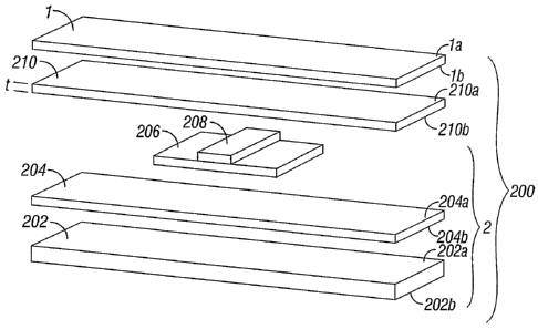
[0049] Referring first to FIG. 4, FIG. 4 illustrates a side view for a
security tag
200 in accordance with one particularly useful embodiment of the present
disclosure.
RFID component 2 includes a base portion or substrate 202 having a first
surface or
surface area 202a and a second surface or surface area 202b which are
typically on
opposing sides of base portion or substrate 202. An antenna 204 is disposed on
the
substrate 202. The antenna 204 has a first surface or surface area 204a and a
second
surface or surface area 204b. which are typically on opposing sides of antenna
204. A
lead frame 206 is disposed on the antenna 204, and an application specific
semiconductor integrated circuit (ASIC) 208 is disposed on the lead frame 206.
First
and second surfaces or surface areas 202a and 202b, 204a and 204b are defined
surface areas of RFID component 2.
[0050] The security tag 200 includes a substantially planar covering material
or
spacer 210 disposed on the RFID component 2 and EAS component 1 disposed on
the
CA 02587150 2007-05-09
WO 2006/055653 PCT/US2005/041573
spacer 210. The spacer 210 has surfaces or surface areas 210a and 210b
disposed on
opposite sides thereof.
[0051] EAS component 1 has a first surface or surface area 1 a and a second
surface or surface area lb which are typically on opposing sides of EAS
component 1.
First and second surfaces or surface areas la and lb are defined surfaces or
surface
areas of EAS component 1.
[0052] For reference purposes, security tag 200 is illustrated as being
disposed
directly underneath EAS component 1, i.e., in position P4 of FIG. 1. The
security tag
200 is shown in position P4 by way of example only and may be disposed in any
position with respect to EAS label 1, as discussed previously with respect to
FIG. 1.
Security tag 200 may also be utilized completely independently of EAS label 1
or in
conjunction therewith. The embodiments are not limited in this context.
[0053] More particularly, security tag 200 includes an EAS component 1 having
one of the defined surface areas 1 a and lb and an RFID component 2 having one
of
the defined surface or surface areas 202a, 202b, 204a and 204b. At least one
of the
defined surface or surface areas la and lb of the EAS component 1 is
configured to at
least partially overlap at least one of the defined surface or surface areas
202a, 202b,
204a and 204b of the RFID component 2. The RFID component 2 may include
antenna 204 which at least partially overlaps at least one of the defined
surfaces or
surface areas la and lb of the EAS component 1.
[0054] In one embodiment, the defined surface or surface area of the RFID
component 2 is one of surface or surface area 202a and 202b.
[0055] The, substantially planar spacer 210 has a thickness "t" and is at
least
partially disposed between at least one of the defined surfaces or surface
areas la and
lb of the EAS component 1 and at least one of the defined surfaces or surface
areas
202a, 202b, 204a, and 204b of the RFID component 2.
[0056] Although FIG. 4 illustrates a limited number of elements, it may be
appreciated that a greater or lesser number of elements may be used for
security tag
200. For example, an adhesive and release liner maybe added to security tag
200 to
assist in attaching security tag 200 to an object to be monitored. Those
skilled in the
art will recognize that semiconductor IC 208 may be directly bonded to antenna
204
without the lead frame 206.
11
CA 02587150 2007-05-09
WO 2006/055653 PCT/US2005/041573
[0057] Returning now to FIG. 3A, RFID system 100 may also include an RFID
reader 102 and security tag 200. Security tag 200 is physically separated from
RFID
reader 102 by a distance dl. As is explained below with respect to FIG. 4,
security
tag 200 is an RFID security tag, tag or label which differs over the prior art
in that it
includes an EAS component, i.e., an EAS label or tag. RFID component 2
includes a
resonant circuit 112. Resonant circuit 112 includes inductor coil L2 with a
resonating
capacitor C2 across the terminals Ti and T2 of ASIC 208. The capacitance of
ASIC
208 is usually negligible compared to C2. If necessary to add additional
capacitance
to the resonant circuit 112 to enable tuning the antenna, i.e., inductor coil
112, to the
proper frequency, a capacitor C2 is connected in parallel to inductor coil L2
so that
resonant circuit 112 becomes a parallel resonant circuit having terminals Ti
and T2
across which an induced voltage V; may be formed. As is explained below with
respect to FIG. 4, terminals Ti and T2 are coupled to other portions of the
RFID
component 2. In addition, the inductance value of inductor coil or antenna L2
includes the inductance presented by the EAS label or tag.
[0058] RFID reader 102 may include a tuned circuit 108 having an inductor L1
which serves as an antenna for RFID reader 102. Where necessary to add
additional
capacitance to the tuned circuit 108 to enable proper tuning of the inductor
coil or
antenna Ll, a capacitor C1 is connected in series with inductor coil or
antenna L1.
RFID reader 102 is configured to produce a pulsed or continuous wave (CW) RF
power across the tuned circuit 108 which is electro-magnetically coupled by
alternating current action to parallel resonant circuit antenna 112 of RFID
component
2. The mutually coupled electro-magnetic power from RFID component 2 is
coupled
to RFID reader 102 through a magnetic field 114.
[0059] RFID component 2 is a power converter circuit that converts some of the
coupled CW RF electro-magnetic power of magnetic field 114 into direct current
signal power for use by the logic circuits of the semiconductor IC used to
implement
the RFID operations for RFID component 2.
[0060] RFID component 2 may also be a RFID security tag which includes
memory to store RFID information and which communicates the stored information
in response to an interrogation signal 104. RFID information may include any
type of
information capable of being stored in a memory used by RFID component 2.
Examples of RFID information include a unique tag identifier, a unique system
12
CA 02587150 2007-05-09
WO 2006/055653 PCT/US2005/041573
identifier, an identifier for the monitored object, and so forth. The types
and amount
of RFID information are not limited in this context.
[0061] RFID component 2 may also be a passive RFID security tag. A passive
RFID security tag does not use an external power source, but rather uses
interrogation
signals 104 as a power source. A detection zone Z1 is defined as an imaginary
volume of space bounded by a generally spherical surface having a radius Rl
generally originating from the inductor Ll. The radius Rl defines a detection
distance or read range R1 such that if distance dl is less than or equal to
read range
Rl, the RFID reader 102 induces a required threshold voltage VT across
terminals Tl
and T2 to activate the RFID component 2. The read range Rl depends on, among
other factors, the strength of the EM field radiation and magnetic field 114
from the
tuned circuit 208. Therefore, the strength of the EM field radiation 114
determines
the read range Rl.
[0062] RFID component 2 may be activated by a direct current voltage that is
developed as a result of rectifying the incoming RF carrier signal including
interrogation signals 104. Once RFID component 2 is activated, it may then
transmit
the information stored in its memory register via response signals 110.
[0063] In general high frequency (HF) operation, when resonant circuit 112 of
RFID system 100 is in proximity to tuned circuit 108 of RFID reader 102, an
alternating current (AC) voltage V; is developed across the terminals Ti and
T2 of
parallel resonant circuit 112 of RFID component 2. The AC voltage V; across
resonant circuit 112 is rectified by a rectifier to a direct current (DC)
voltage and
when the magnitude of the rectified voltage reaches a threshold value VT, RFID
component 2 is activated. The rectifier is the aforementioned application
specific
integrated circuit (ASIC) 208. Once activated, the RFID component 2 sends
stored
data in its memory register by modulating interrogation signals 104 of RFID
reader
102 to form response signals 110. The RFID device 106 then transmits the
response
signals 110 to the RFID reader 102. RFID reader 102 receives response signals
110
and converts them into a detected serial data word bitstream of data
representative of
the information from RFID component 2.
[0064] The RFID system 100 as illustrated in FIG. 3A may be considered to be a
high frequency (IF) RFID system because the RFID reader 102 couples
inductively
13
CA 02587150 2007-05-09
WO 2006/055653 PCT/US2005/041573
to the RFID component 2 via magnetic field 114. In HF applications, antenna
204 is
typically an inductance coil type antenna as provided by inductance coil L2.
[0065] FIG. 3B illustrates an ultrahigh frequency (UHF) RFID system 150 in
which an RFID reader 152 couples to an RFID device, tag or label 156 at a
distance
d2 away via an electric field E. The frequency band for UHF is considered
herein to
range from about 300 MHz to about 3 GHz. The UHF range specifically includes
frequencies in the 868 MHz band, the 915 MHz band, and the 950 MHz band.
[0066] For UHF applications, antenna 204 of RFID component 2 typically
includes a UHF open-ended dipole antenna while the RFID reader 152 typically
includes a patch antenna. A coaxial feed line from the reader 152 is connected
to the
patch antenna. The UHF antenna may be a simple half-wave dipole or a patch
antenna. Many popular designs use an air filled cavity backed patch antenna
which
can be either linearly polarized or circularly polarized. The electric field
vectors E1
and E2 rotate with equal magnitude for the circularly polarized case. The
linearly
polarized antenna has higher magnitudes of E field in certain orthogonal
orientations,
which may be suitable for certain RFID label orientations.
[0067] Therefore, in UHF applications, the antenna 204 of RFID component 2
includes an open-ended dipole antenna while in HF applications, is typically
inductor
L2.
[0068] In general, when operating in the UHF range, it is not necessary for
the
RFID component 2 to include a capacitor such as C2 in parallel with the open-
ended
dipole antenna 204 to enable tuning to the frequency transmitted by the patch
antenna
of RFID reader 152.
[0069] Returning to FIG. 4, as previously noted, RFID component 2 may include
a base portion or substrate 202 which includes any type of material suitable
for
mounting antenna 204, lead frame 206, and IC 208. For example, material for
substrate 202 may include base paper, polyethylene, polyester,
polyethyleneterephthalate (PET), polyetherimide (PEI) (e.g., ULTEM amorphous
thermoplastic PEI sold by the General Electric Co. of Fairfield, Connecticut)
and/or
other materials. It is known that the particular material implemented for
substrate 202
may impact the RF performance of security tag 200 and, as such, the dielectric
constant and the loss tangent may characterize the dielectric properties of an
appropriate substrate material for use as substrate 202.
14
CA 02587150 2007-05-09
WO 2006/055653 PCT/US2005/041573
[0070] In general, a higher dielectric constant may cause a larger frequency
shift
of an antenna when compared to free space with no substrate present. Although
it
may be possible to re-tune the antenna to the original center frequency by
physically
changing the antenna pattern, it may be desirable to have a material with a
high
dielectric constant and with a low dielectric loss since usage of such a
material results
in a smaller tag or label size. The term "read range" may refer to the
communication
operating distance between RFID reader 102 and security tag 200. An example of
a
read range for security tag 200 may range from 1-3 meters, although the
embodiments
are not limited in this context. The loss tangent may characterize the
absorption of RF
energy by the dielectric. The absorbed energy may be lost as heat and may be
unavailable for use by ASIC 208. The lost energy may result in the same effect
as
reducing the transmitted power and may reduce the read range accordingly.
Consequently, it may be desirable to have the lowest loss tangent possible in
substrate
202 since it cannot be "tuned out" by adjusting antenna 204. The total
frequency shift
and RF loss may depend also on the thickness of substrate 202. As the
thickness
increases, the shift and loss may also increase.
[0071] In one embodiment, for example, substrate 202 may be configured using
base paper having a dielectric constant of about 3.3, and a loss tangent of
about 0.135.
The base paper may be relatively lossy at 900 MHz. A lossy material has a
dielectric
loss factor greater than about 0.01. In one embodiment, substrate 202 may be
configured of plastic having a dielectric constant of about 3.3 and a loss
tangent of
less than about 0.01. The embodiments are not limited in this context.
[0072] In one embodiment, security tag 200 may include IC 208 having a
semiconductor IC, such as an RF1D chip or application specific integrated
circuit
(ASIC) ("RFID chip"). RFID chip 208 may include, for example, an RF or
alternating current (AC) rectifier that converts RF or AC voltage to DC
voltage, a
modulation circuit that is used to transmit stored data to the RFID reader, a
memory
circuit that stores information, and a logic circuit that controls overall
function of the
device. In one embodiment, RFID chip 208 may be configured to use an I-CODE
High Frequency Smart Label (HSL) RFID ASIC or a U-CODE Ultrahigh Frequency
Smart Label (USL) RFID ASIC, both of which are made by Philips Semiconductor
of
Amsterdam, the Netherlands, or an XRAOO RFID chip made by ST Microelectronics
of Geneva, Switzerland. The embodiments, however, are not limited in this
context.
CA 02587150 2007-05-09
WO 2006/055653 PCT/US2005/041573
[0073] Lead frames are small connections which enable attaching an RFID chip
such as RFID chip 208 to an antenna such as antenna 204. In one embodiment,
RFID
chip 208 may be directly bonded to antenna 204 without including lead frame
206.
Lead frame 206 may also include a die mounting paddle or flag, and multiple
lead
fingers. The die paddle primarily serves to mechanically support the die
during
package manufacture. The lead fingers connect the die to the circuitry
external to the
package. One end of each lead finger is typically connected to a bond pad on
the die
by wire bonds or tape automated bonds. The other end of each lead finger is
the lead,
which is mechanically and electrically connected to a substrate or circuit
board. Lead
frame 206 may be constructed from sheet metal by stamping or etching, often
followed by a finish such as plating, downset and taping. In one embodiment,
for
example, lead frame 206 may be implemented using a Sensormatic EAS
MicrolabelTM
lead frame made by Sensormatic Corporation, a division of Tyco Fire and
Security,
LLC, of Boca Raton, Florida, for example. The embodiments, however, are not
limited in this context.
[0074] In one embodiment, antenna 204 includes the inductor coil L2, and when
required, the capacitor C2, of resonant circuit 112 of RFID component 2. The
terminals Ti and T2 are also included in antenna 204 to couple to the RFID
chip 208
to enable the induced voltage V; to activate the RFID component 2 once the
threshold
voltage VT is reached.
[0075] In one embodiment, antenna 204 includes typically the open ended dipole
antenna of RFID component 2 for UHF applications. Terminals T1 and T2 may also
be included in antenna 204 to couple to the RFID chip 208 to enable the
electric field
E to excite the antenna of reader 152
[0076] In one embodiment, security tag 200 may also include covering or spacer
material 210 applied to the top of a finished security tag. As with substrate
202,
covering or spacer material 210 may also impact the RF performance of RFID
component 2. For example, covering material 210 may be implemented using cover
stock material having a dielectric constant of about 3.8 and a loss tangent of
about
0.115. The embodiments are not limited in this context.
[0077] More particularly, as previously mentioned, the substantially planar
spacer
210 has a thickness "t". The thickness "t" is generally about 1 mm to 2 mm
when the
security tag 200 is a hard combination tag and considerably less than 1 mm
when the
16
CA 02587150 2007-05-09
WO 2006/055653 PCT/US2005/041573
security tag 200 is a combination label. As previously mentioned, the spacer
210 has
surfaces or surface areas 210a and 210b disposed on opposite sides thereof. In
one
embodiment, spacer surfaces or surface areas 21 Oa and 21Ob are parallel to
each
other. EAS component 1 at least partially overlaps at least one of the spacer
surfaces
or surface areas 210a and 210b.
[0078] An RFID insert is a term common in the art and may be defined herein as
the RFID component 2, which includes the combination of substrate 202, antenna
204, lead frame 206 if applicable, and RFID chip 208. RFID component 2 at
least
partially overlaps another one of the spacer surfaces 210b. Security tag 200
includes
RFID insert or component 2 and spacer 210.
[0079] Security tag 200 may also include antenna 204. Antenna 204 may be
representative of, for example, antenna 112 of RFID device 106 or antenna 204
may
be formed by a parallel resonant LC circuit, where L is inductance and C is
capacitance. Alternatively, antenna 204 may also be a tunable antenna which is
tuned
to the carrier signal so that the voltage across the antenna circuit is
maximized. As
can be appreciated this will increase the read range of antenna 204. It is
known that
the degree of preciseness of the tuning circuit is related to the spectrum
width of the
carrier signal transmitted by transmitter 102. For example, in the United
States, the
Federal Communication Commission currently (FCC) regulates one band of the
RFID
security tag spectrum to 915 MHz. Therefore, transmitter 102 should transmit
interrogation signals 104 at approximately 915 MHz. To receive interrogation
signals
104, antenna 204 should be narrowly tuned to the 915 MHz signal. For 915 MHz
applications, the RFID tag antenna 204 may be printed, etched or plated.
[0080] The EAS label 1 creates or presents a constant load impedance to RFID
component 2. As a result, antenna 204 of RFID label 200 uses this constant
load of
EAS label 1 for impedance matching. More particularly, antenna 204 has a
complex
impedance and the EAS component 1 forms a part of an impedance matching
network
of the antenna. Therefore, the impedance of antenna 204 includes the loading
effect
of the EAS component 1. That is, the loading effects of the EAS component 1
are the
constant load impedance of the EAS component 1. The loading effect of EAS
component 1 may be varied by substituting or exchanging one material included
within the EAS component 1 having one dielectric constant and loss tangent for
another material having another dielectric constant and loss tangent.
17
CA 02587150 2007-05-09
WO 2006/055653 PCT/US2005/041573
[0081] The RFID component chip 208 may be represented as an equivalent series
RC circuit, where R represents a resistor and C represents a capacitor. This
circuit is
represented by a complex impedance Zchip as
'chip - Z1 jZ ,
where Zl and Z2 are the real and imaginary components of the impedance of
the chip 208. The RFID device tag or label antenna 204 may be represented by a
complex impedance Zantenna as
Zantenna Z3 + jZ (1 ~
where Z3 and Z4 are the real and imaginary components of the impedance of
the antenna 204. When the chip 208 is mounted on the antenna 204, the complex
impedance of chip 208 is matched to the coupled conjugate impedance of the
RFID
antenna 204, including the impedance matching effect or loading effect of the
EAS
component or label 1. This allows maximum power coupling to the RFID chip 208
which results in the greatest read range Rl.
[0082] In one embodiment, thickness "t" of spacer 210 may be varied to vary
with
respect to either the RFID reader device 102 or to the RFID reader device 152
in order
to vary the read range RI, respectively. More particularly, thickness "t"
determines
the read range, i.e., the maximum distance Rl between the security tag 200 and
the
EAS/RFID reader 102 or the EAS/RFID reader 152 at which the reader 102 or 152
may interrogate the security tag 200. The read range Rl is affected adversely
as
thickness "t" decreases. Conversely, the read range R1 increases as thickness
"t"
increases. It should be noted that reader 102 for HF applications and reader
152 for
UHF either read only the EAS component 1 or only the RFID component 2 such
that
the EAS component 1 is read by a dedicated EAS reader while RFID component 2
is
read by a dedicated RFID reader. Alternatively, reader 102 and reader 152 may
be
combined in the same housing or their functions integrated to be performed by
the
same hardware. Undesirable interference between the reading of EAS component 1
and the reading of RFID component 2 is prevented or minimized because of the
wide
discrepancy between the range of read frequencies common to EAS components as
opposed the range of read frequencies common to RFID components, with the EAS
components typically being read at frequencies in the range of less than or
equal to t
8.2 KHz, whereas RFID components are typically being read at frequencies in
the
range of 13 MHz or greater.
18
CA 02587150 2007-05-09
WO 2006/055653 PCT/US2005/041573
[0083] However, it is envisioned that since security tags 200 and 400 are
stand
alone devices, security tags 200 and 400 provide an EAS function and an RFID
function independently of the type of reader or readers or particular
frequencies to
which security tags 200 or 400 are subjected.
[0084] The spacer 210 is made using a low loss, low dielectric material such
as
ECCOSTOCK RH rigid foam, made by Emerson Cuming Microwave Products, Inc.
of Randolph, Massachusetts, or any other similar material. The embodiments are
not
limited in this context. When made from one of the foregoing materials, the
read
range is about 30.5 to 61.0 cm (1 to 2 feet) when the thickness "t" of spacer
902 is
about 0.0762 mm (0.003 inches). Similarly, the read range is about 127 cm (5
feet)
when the thickness "t" of spacer 210 is at least 1.02 mm (0.040 inches).
[0085] In one embodiment, the spacer 210 may be a thin film having a thickness
"t" of about 0.05 mm where EAS component 1 directly overlaps RFID component 2.
[0086] In one embodiment, the spacer may be air where the EAS label 1 is
supported mechanically away from the RFID component 2.
[0087] As a result, security tag 200 provides significant advantages over the
prior
art by enabling a combined EAS/RFID devices of significantly lower space or
volume
and lower cost.
[0088] In one embodiment, security tag 200 may use an induced voltage from a
coil antenna for operation. This induced AC voltage may be rectified to result
in a
DC voltage. As the DC voltage reaches a certain level, the RFID component 2
begins
operating. By providing an energizing RF signal via transmitter 102, RFID
reader
102 can communicate with a remotely located security tag 200 that has no
external
power source such as a battery.
[0089] Since the energizing and communication between the RFID reader and
RFID component 2 is accomplished through antenna 204, antenna 204 may be tuned
for improved RFID applications. An RF signal can be radiated or received
effectively
if the linear dimension of the antenna is comparable with the wavelength of
the
operating frequency. The linear dimension, however, may be greater than the
available surface area available for antenna 204. Therefore, it may prove
difficult to
utilize a true full size antenna in a limited space which is true for most
RFID systems
in HF applications. Accordingly, it is contemplated that RFID component 2 may
use
a smaller LC loop antenna circuit that is arranged to resonate at a given
operating
19
CA 02587150 2007-05-09
WO 2006/055653 PCT/US2005/041573
frequency. The LC loop antenna may include, for example, a spiral coil and a
capacitor. The spiral coil is typically formed by n-turns of wire, or n-turns
of a
printed or etched inductor on a dielectric substrate.
[00901 For HF applications, in order to achieve good RFID coupling, the loop
area*turns product and resonant frequency need to be optimized. In one
embodiment
of the present disclosure illustrated in FIG. 3A, the resonant frequency can
be effected
by tuning the parallel capacitor C2 of the resonant circuit 112 including the
effects on
impedance of the EAS label 1 and of the RFID chip 208.
[00911 In either HF or UHF applications, for the particular frequency of
interest,
the RFID chip complex impedance must be matched by the complex conjugate
impedance of the antenna including the loading effects on impedance of the EAS
label. In the BF case, a resonating capacitor is commonly used to tune the
frequency.
This capacitor is usually larger than the RFID chip capacitance and will
dominate the
response. For the UHF case, the RFID chip complex impedance contains only the
chip capacitance for tuning.
[00921 In another embodiment according to the present disclosure, antenna 204
may be designed so that the complex conjugate of the overall antenna matches
the
impedance to the complex impedance of lead frame 206 and IC 208 at the desired
operating frequency, e.g., 915 MHz. When RFID security tag 200 is placed on an
object to be monitored, however, it has been observed that the resulting
operating
frequency may change, i.e., each object may have a substrate material with
dielectric
properties affecting the RF performance of antenna 204. In other words and as
with
substrate 202, the object substrate may cause frequency shifts and RF losses
determined by the dielectric constant, loss tangent, and material thickness.
Examples
of different object substrates may include so called "chip board" (i.e.,
material used
for item-level cartons, corrugated fiber board which is material used for
corrugated
boxes), video cassette and digital video disc (DVD) cases, glass, metal, etc.
It is
contemplated that each object substrate may have a significant effect on the
read
range Rl for security tag 200.
[00931 Antenna 204 may be tunable to compensate for such variations. In other
words, since the dielectric constant for many materials is greater than one,
the
operating frequency is typically lowered when security tag 200 is attached to
an
object substrate. In order to establish the original frequency, antenna 204 is
typically
CA 02587150 2007-05-09
WO 2006/055653 PCT/US2005/041573
altered in some manner, otherwise detection performance and read range may be
reduced. As such, antenna 204 may be altered by trimming the ends of antenna
204
by severing the antenna conductor and isolating the resultant trimmed antenna
segment from the ends that were cut away. The trimmed ends do not necessarily
have
to be removed to allow the tuning operation. Consequently, continuous tuning
of
antenna 204 to the desired operating frequency is possible to allow operation
of
security tag 200 when security tag 200 is attached to different objects.
Security tag
200 in general, and antenna 204 in particular, are described in more detail
below with
reference to FIGS. 5-7.
[0094] FIG. 5 illustrates a top view of a partial security tag 200 with an
antenna in
accordance with one embodiment according to the present disclosure which is
particularly suitable for UHF applications. Security tag 200 includes antenna
204
disposed upon substrate 202 which is substantially rectangular in shapes. In
one
envisioned embodiment, antenna 204 is disposed on substrate 202 by die-cutting
the
label antenna pattern onto substrate 202.
[0095] RFID chip 208 may be connected to lead frame 206 by ultrasonically
bonding lead frame 206 to the conductive pads on RFID chip 208. In the
particular
embodiment of FIG. 5, RFID chip 208 and lead frame 206 are placed in the
geometric
center of the dielectric substrate material of substrate 202. The ends of lead
frame
206 are mechanically and electrically bonded to the foil antenna pattern of
antenna
204. A covering material (not shown) may be applied over the entire top
surface of
security tag 200 to protect the assembly and provide a surface for printing
indicia if
desired. It is known in the art to use an anisotropic electrically conductive
thermally
setting adhesive to bond the RFID chip 208 to the antenna 204. An example of
such
an adhesive is Loctite 383 made by the Henkel Loctite Corporation of Rocky
Hill,
Connecticut. Antenna 204 may also include multiple antenna portions. For
example,
antenna 204 may include a first antenna portion 306 and a second antenna
portion
308, the first antenna portion 306 being connected to a first side 206A of
lead frame
206, and the second antenna portion 308 connected to a second side 206B of
lead
frame 206. Therefore, antenna 204 is the entire RFID tag antenna which is
subdivided into first antenna portion 306 and second antenna portion 308.
[0096] First antenna portion 306 may have a first antenna end 306A and a
second
antenna end 306B. Similarly, second antenna portion 308 may have a first
antenna
21
CA 02587150 2010-06-30
77496-245
end 308A and a second antenna end 308B. In one embodiment and as shown in FIG.
5, first antenna end 306A of first antenna portion 306 is connected to lead
frame
206A. First antenna portion 306 is disposed on substrate 202 to form an
inwardly
spiral pattern from RFID chip 208 in a first direction, with second antenna
end 306B
positioned to terminate on the inner loop of the inwardly spiral pattern.
Similarly,
first antenna end 308A of second antenna portion 308 may be connected to lead
frame
206B. Second antenna portion 308 is also disposed on substrate 202 to form an
inwardly spiral pattern from RFID chip 208 in a second direction, with second
antenna end 308B positioned to terminate on the inner loop of the inwardly
spiral
pattern.
[00971 In one embodiment, the antenna geometry of antenna 204 is configured to
traverse around the perimeter of substrate 202 and spiral inwardly. It is
envisioned
that the inwardly directed spiral antenna pattern may provide several
advantages:
[00981 (1) The ends of antenna 204 may be placed well inside the perimeter of
substrate 202. Placing the ends of antenna 204 within the perimeter of
substrate 202
may allow the ends to be trimmed without changing the amount of area used by
antenna 204;
[00991 (2) The Q factor of antenna 204 may be optimized so that the response
of
security tag 200, including the effects of spacer 210 and EAS label 1, only
varies by
approximately -3 dB at the ISM band limits. Using the Chu-Harrington limit of
Q =
11(ka)3 + 1/(ka), where k = 27r/ and "a" is a characteristic dimension of
antenna 204,
it can be seen that a sphere of radius "a" could just enclose security tag
200. For a
high Q factor, then "ka" should be << 1. Therefore, by maximizing Q, "a" is
minimized to fall within the operating frequency band limits. The tuning of
antenna
204 for UHF applications is disclosed in further detail in co-pending,
commonly
owned U.S. Patent Application Publication No. 2006-0033624 filed on August 13,
2004
entitled "TUNABLE ANTENNA" by R. Copeland and G. M. Shafer
1001001 Antenna 204 may also be tuned particularly for UHF applications to a
desired operating frequency by modifying a first length for first antenna
portion 306,
and a second length for second antenna portion 308, after these antenna
portions are
disposed on substrate 202. For example, each antenna portion may be divided
into
multiple antenna segments at multiple segment points. The fast and second
antenna
22
CA 02587150 2007-05-09
WO 2006/055653 PCT/US2005/041573
lengths may be modified by electrically isolating at least a first antenna
segment from
a second antenna segment. The antenna length may be modified by severing each
antenna portion at one of multiple segment points, with each segment point to
correspond to an operating frequency for antenna 204. Dividing first antenna
portion
306 and second antenna portion 308 into multiple antenna segments results in
shortening the length of each antenna portion, and thereby effectively changes
the
total inductance of antenna 204. The antenna segments and segment points are
described in more detail with reference to FIG. 6.
[00101] FIG. 6 illustrates a diagram of a security tag 400 with an antenna
having
segment points in accordance with one embodiment. In particular, FIG. 6
illustrates a
top view of portions of security tag 400 with multiple segment points SP1,
SP2, SP3
and SP4. In a similar manner as shown in FIG. 4 with respect to security tag
200,
security tag 400 may include EAS component 1, spacer 210 and RFID component 2.
Antenna 204 may be tuned also to a desired operating frequency by modifying a
first
length for first antenna portion 306, and a second length for second antenna
portion
308, after these antenna portions are disposed on substrate 202. For example,
it is
contemplated that each antenna portion may be divided into multiple antenna
segments at multiple segment points SP 1 -SP4. Multiple segment points SP 1
through
SP4 represent end tuning positions where the antenna 204 may be cut or trimmed
in
order to be tuned to various objects. SP1 is the free space position where the
length of
original free space antenna 204 is tuned to 868 MHz. SP2 is the free space
position
where the length of antenna portions 306 and 308 is tuned to 915 MHz. SP3 and
SP4
are the free space positions where the length of antenna portions 306 and 308
is tuned
to the various objects. The various objects include, for example and are not
limited
to, retail and/or wholesale merchandise.
[00102] The first and second antenna lengths may be modified by electrically
isolating at least a first antenna segment from a second antenna segment. The
antenna
length may be modified by severing each antenna portion at one of multiple
segment
points, with each segment to correspond to an operating frequency for antenna
204.
The severing may be achieved in a number of different ways, such as cutting or
punching the antenna trace at a given segment point SP 1-SP4. The severing may
create a slot at the segment point, such as slots 402, 404, 406, 408, 410, and
412.
23
CA 02587150 2007-05-09
WO 2006/055653 PCT/US2005/041573
[00103] It should be noted that for HF applications, antenna 204 is tuned by
changing the inductance or capacitance parameters but not the lengths of the
segments.
[00104] In one embodiment, and as shown in FIG. 6, each segment point SP1-SP4
corresponds to an operating frequency for antenna 204. In one example, SP1 may
tune antenna 204 for an operating frequency of approximately 868 MHz when
security tag 400 is in free space and unattached to an object. SP2 may tune
antenna
204 for an operating frequency of approximately 915 MHz when security tag 400
is in
free space and unattached to an object. SP3 may tune antenna 204 for an
operating
frequency of approximately 915 MHz when security tag 400 is attached to a VHS
cassette housing. SP4 may tune antenna 204 for an operating frequency of
approximately 915 MHz when -security tag 400 is attached to a chip board. As
can be
appreciated, the number of segment points and corresponding operating
frequencies
for antenna 204 may vary according to a given implementation. The embodiments
are
not limited in this context.
[00105] FIG. 7 illustrates a block flow diagram 500 in accordance with another
embodiment of the present invention. As mentioned above, security tag 200 may
be
configured in a number of different ways. For example: 1) an integrated
circuit may
be connected to a lead frame at block 502; 2) an antenna may be disposed on a
substrate at block 504; 3) the lead frame may be connected to the antenna at
block
506.
[00106] In one particular embodiment, the antenna is tuned for use with an
operating frequency at block 508. The tuning may be performed by modifying a
length for the antenna by severing the antenna into multiple antenna segments
at a
segment point corresponding to the operating frequency. The severing may
electrically disconnect a first antenna segment from a second antenna segment,
thereby effectively shortening the length of the antenna.
[00107] As described above, the unique antenna geometry of an inwardly spiral
pattern may be useful for RFID applications when connected to an RFID chip. As
previously noted, the unique antenna geometry shown in FIGS. 5 and 6, however,
may also be useful for an EAS system where security tag 200 and security tag
400,
respectively, each include EAS component 1 and spacer 210. In one embodiment,
RFID chip 208 may be replaced with a diode or other non-linear passive device
where
24
CA 02587150 2007-05-09
WO 2006/055653 PCT/US2005/041573
the voltage and current characteristics are non-linear. The antenna for the
diode or
other passive non-linear EAS device may have the same geometry as shown in
FIGS.
and 6, and may be trimmed to tune the antenna to the operating frequency of
the
transmitter used to transmit interrogation signals for the EAS system. Similar
to
5 RFID system 100, the range of operating frequencies may vary, although the
embodiments may be particularly useful for the UHF spectrum, such as 868-950
MHz. The embodiments are not limited in this context.
[00108] It is also contemplated that some embodiments of the present
disclosure
may be configured using an architecture that may vary in accordance with any
number of factors, such as: 1) desired computational rate; 2) power levels; 3)
heat
tolerances; 4) processing cycle budget; 5) input data rates; 6) output data
rates; 7)
memory resources; 8) data bus speeds and other performance constraints. For
example, an embodiment may be configured using software executed by a general-
purpose or special-purpose processor. In another example, an embodiment may be
configured as dedicated hardware, such as a circuit, an ASIC, Programmable
Logic
Device (PLD) or a digital signal processor (DSP). In yet another example, an
embodiment may be configured by any combination of programmed general-purpose
computer components and custom hardware components. The embodiments are not
limited in this context.
[00109] Examples of security tags 200 and 400, which are combination EAS and
RFID labels / tags, are shown in FIGS. 8A to 8D which show various types of
adhesive magnetostrictive labels and EAS hard tags, such as the SuperTag
produced
by Sensormatic, a division of Tyco Fire and Security, LLC of Boca Raton,
Florida.
FIG. 8A illustrates an EAS label 804 adjacent to an RFID label 806 in a co-
planar
configuration. This configuration of adjacent labels 804 and 806 is known in
the prior
art. FIG. 8B illustrates a variation of the co-planar configuration of EAS
label 804
and RFID label 806 of FIG. 8A wherein the EAS label 804 and the RFID label 806
are separated from each other by a gap 805 having a distance "g". This
configuration
of 804 and 806 being separated by gap 805 is also known in the prior art.
[00110] In both the configuration of FIG. 8A and 8B, the EAS label 804 and the
RFID label 806 act independently of one another with respect to matching of
impedance values. As "g" increases, the read range increases. As a result, the
size of
gap "g" controls the impedance load. However, this is not a desirable effect
because
CA 02587150 2007-05-09
WO 2006/055653 PCT/US2005/041573
although the read range increases, the total area occupied by the EAS label
804 and
RFID label 806 increases, necessarily occupying more space or area on an
object to
be identified.
[00111] FIG. 8C illustrates an embodiment of the present disclosure of a
security
tag 200 or 400 showing an EAS component or label 1. An RFID component or
insert
2 is mounted directly underneath the EAS component or label 1. A dummy bar
code
802 is printed on the EAS component or label 1 and is just for visual purposes
only.
Dummy bar code 802 has no EAS or RFID function. As compared to the prior art,
the configuration of security tag 200 or 400 as a combination EAS component or
label
or tag 1 with RFID component or insert 2 mounted directly underneath the EAS
component or label 1 (as shown in FIG. 4) provides a minimal separation
between the
RFID component or insert 2 and the EAS label 1.
[00112] FIG. 8D illustrates one embodiment of the present disclosure of one
portion 812 of a housing for combination EAS component or label 1 with RFID
component or insert 2. The RFID component or insert 2 is defined as including
RFID
chip 208 mounted on antenna 204. However, spacer 210 or an adhesive layer are
not
visible (See FIG. 4).
[00113] FIG. 8E is an elevation view of the combination EAS component or label
1
with RFID component or insert 2 disclosed in FIG. 8D, but showing spacer 210
disposed between the EAS component or label 1 and the RFID component or insert
2.
[00114] FIG. 8F illustrates one embodiment of the present disclosure of one
portion 818 of a housing for a combination EAS label 816 similar to EAS
component
or label 1 with an RFID insert 814 which is similar to RFID component or
insert 2.
The RFID insert 814 is defined as another RFID chip 820 mounted on antenna
204.
Again, spacer 210 or an adhesive layer are not visible (See FIG. 4).
[00115] FIG. 8G is an elevation view of the combination EAS label 816 with
RFID
insert 814 disclosed in FIG. 8F, but showing spacer 210 disposed between the
EAS
label 816 and the RFID insert 814.
[00116] The types of EAS devices and RFID combinations are not limited to the
EAS and RFID devices described herein.
[00117] While certain features of the embodiments have been illustrated as
described herein, many modifications, substitutions, changes and equivalents
will now
occur to those skilled in the art. It is therefore to be understood that the
appended
26
CA 02587150 2007-05-09
WO 2006/055653 PCT/US2005/041573
claims are intended to cover all such modifications and changes as fall within
the true
spirit of the embodiments.
27