Note : Les descriptions sont présentées dans la langue officielle dans laquelle elles ont été soumises.
CA 02587871 2007-05-17
WO 2006/057887 PCT/US2005/041678
H-BRIDGE ACTIVATOR/DEACTIVATOR AND METHOD
FOR ACTIVATING/DEACTIVATING EAS TAGS
CROSS-REFERENCE TO RELATED APPLICATIONS
[0001] This application claims the benefit of priority under 35 U.S.C. 119 to
U.S.
Provisional Patent Application 60/629,956 filed on November 22, 2004 entitled
"H-
Bridge Deactivator", the entire contents of which is incorporated by reference
herein.
BACKGROUND OF THE INVENTION
1. Field of the Invention
[0002] This invention relates to an H-bridge deactivator that utilizes an H-
bridge
switch network to perform activation, deactivation or reactivation of an
electronic article
surveillance (EAS) tag and particularly to activation, deactivation or
reactivation of an
acoustomagnetically activated EAS tag.
2. Description of the Related Art
[0003] Acoustomagnetically activated EAS tags are typically demagnetized by a
strong
magnetic alternating field with a slowly decaying field strength, Conversely,
acoustomagnetically activated EAS tags can only be initially activated or
subsequently
reactivated by magnetizing with a strong constantly positive or constantly
negative
magnetic field with a slowly decaying field strength.
[0004] Therefore, existing acoustomagnetic (AM) deactivators require either
high
voltage (110VAC - volts alternating current) or very high voltage (200-500VDC -
volts
direct current) in order to generate the high currents required to produce a
magnetic field
of sufficient magnitude to deactivate an EAS tag. The voltages required impose
special
safety concerns that tend to constrain the design. Furthermore, if power is
interrupted or
lost, the deactivator will not work for that period of time and such
deactivators are not
portable. The prior solutions address uninterruptible power and portability
regarding a
small handheld deactivator, but not for a large deactivator or a low voltage
deactivator.
1
CA 02587871 2007-05-17
WO 2006/057887 PCT/US2005/041678
SUMMARY
[0005] It is an object of the present disclosure to provide an alternate
method for
activation, deactivation, or reactivation of an EAS acoustomagnetically
activated tag by
utilizing an H-bridge circuit to generate the alternating and decaying
currents required for
activation, deactivation or reactivation.
[0006] It is another object of the disclosure to enable low voltage
activation,
deactivation or reactivation of an EAS tag, e.g., at voltage levels of 12 to
24VDC.
[0007] Still another object of the present disclosure is to ensure
uninterruptible power
for activation, deactivation or reactivation of an EAS tag in case of loss of
external
power.
[0008] It is yet another object of the present disclosure to provide a
portable apparatus
for activation, deactivation or reactivation of an EAS tag.
[0009] For example, in one embodiment of the present disclosure, activation,
deactivation or reactivation of an EAS tag is accomplished without a high
voltage
capacitor that is required typically in large deactivation designs, thereby
lowering cost
and enhancing safety.
[0010] It is an object of the present disclosure to provide alternate methods
of
activation, deactivation or reactivation so that a designer may optimize for a
particular
environment.
[0011] In particular, the present disclosure is directed to an apparatus for
activating,
deactivating or reactivating an electronic article surveillance (EAS) tag by
means of an H-
bridge circuit coupled to an antenna. The H-bridge circuit is adapted to
connect to a
source of current to the circuit and is configured to direct an increasing
current flow
through the antenna in a first direction, thereby generating a positive
increasing magnetic
field from the antenna. In one particularly useful embodiment, the H-bridge is
configured
to direct a decreasing current flow through the antenna in the first
direction, thereby
generating a positive decreasing magnetic field from the antenna. The H-bridge
circuit
may also be configured to direct an increasing current flow through the
antenna in a
second direction such that the direction of current flow through the antenna
reverses,
thereby generating a negative increasing magnetic field from the antenna. In
another
particularly useful embodiment, the H-bridge circuit is configured to direct a
decreasing
current flow through the antenna in the second direction, thereby generating a
negative
decreasing magnetic field from the antenna.
2
CA 02587871 2007-05-17
WO 2006/057887 PCT/US2005/041678
[0012] In one embodiment, the circuit includes at least four switches and an
antenna
having first and second ends for directing current through the antenna. The
first and third
switches are coupled to a first junction, and the second and fourth switches
are coupled to
a second junction. The first and fourth switches are coupled to a third
junction, and the
second and third switches are coupled to'a fourth junction. The first end of
the antenna is
coupled to the third junction, and the second end of the antenna is coupled to
the fourth
junction. As a result, the first switch controls current between the first
junction and the
third junction, the second switch controls current between the second junction
and the
fourth junction, the third switch controls current between the first junction
and the fourth
junction, and the fourth switch controls current between the second junction
and the third
junction.
[0013] The apparatus may also include a circuit controller controlling the
circuit to
generate in at least a first cycle a positive increasing magnetic field from
the antenna.
More particularly, following connection of a source of DC power between the
first and
second junctions, the circuit controller opens the third and fourth switches,
and closes the
first switch to direct current from the first junction to the third junction;
and closes the
second switch to direct current from the fourth junction to the second
junction, thereby
directing an increasing current through the antenna in a first direction from
the third
junction to the fourth junction. The circuit controller may also be configured
to further
control the circuit to generate in the first cycle a positive decreasing
magnetic field from
the antenna by: disconnecting the source of DC power between the first and
second
junctions; opening the first, third and fourth switches; and closing the
second switch,
thereby directing a decreasing current through the antenna in the first
direction from the
third junction to the fourth junction.
[0014] The circuit controller may be particularly configured to continue to
control the
circuit to generate in the at least a first cycle a negative increasing
magnetic field from the
antenna. More particularly, upon connecting a source of DC power between the
first and
second junctions, the circuit controller opens the first and second switches,
and closes the
third switch to direct current from the first junction to the fourth junction;
and closes the
fourth switch to direct current from the third junction to the second
junction, thereby
directing increasing current through the antenna in a second direction from
the fourth
junction to the third junction.
[0015] The circuit controller may also be configured to control the circuit to
generate in
at least the first cycle a negative decreasing magnetic field from the
antenna. More
3
CA 02587871 2007-05-17
WO 2006/057887 PCT/US2005/041678
particularly, upon disconnecting the source of DC power between the first and
second
junctions, the circuit controller opens the first, second and third switches;
and closes the
fourth switch, thereby directing decreasing current through the antenna in the
second
direction from the fourth junction to the third junction.
[0016] It is envisioned that second and succeeding cycles repeat in a similar
manner the
actions occurring during the first cycle, i.e., generating a positive
increasing magnetic
field, generating a positive decreasing magnetic field, generating a negative
increasing
magnetic field and generating a negative decreasing magnetic field. It is
contemplated
that the cycle time of the first cycle exceeds cycle time of the second cycle,
and the cycle
time of each succeeding cycle consecutively decreases with respect to the
cycle time of
the second cycle.
[0017] Typically, the antenna is an inductance coil antenna and the switches
are high
current transistors or field effect transistors. The current source may
include an AC/DC
converter providing DC output, with the AC/DC converter being coupled to a
source of
AC power. The current source may further include a DC/DC High Voltage
converter
coupled to the AC/DC converter, with the DC/DC High Voltage converter
providing DC
High Voltage output. Alternatively, the current source may include a battery,
or may
further include an AC/DC charger coupled to the battery to provide DC output,
with the
AC/DC charger being coupled to a source of AC power.
[0018] The DC output of the AC/DC converter may be either 12 VDC, 24 VDC, or
110
VDC. The DC High Voltage output from the DC/DC High Voltage converter may be
greater than 110 VDC. The voltage output of the battery may be either 12 VDC
or 24
VDC. The voltage output of the AC/ DC charger may be either 12 VDC or 24 VDC.
The
source of AC power may be 110 to 120 VAC.
[0019] In addition, the present disclosure is directed to a method of
deactivating an
electronic article surveillance (EAS) tag which includes the steps of:
providing an H-
bridge circuit coupled to an antenna; applying a source of current to the H-
bridge circuit;
directing an increasing current flow through the antenna in a first direction,
thereby
generating a positive increasing magnetic field from the antenna; directing a
decreasing
current flow through the antenna in the first direction, thereby generating a
positive
decreasing magnetic field from the antenna; directing an increasing current
flow through
the antenna in a second direction such that current flow through the antenna
reverses,
thereby generating a negative increasing magnetic field from the antenna; and
directing a
decreasing current flow through the antenna in the second direction, thereby
generating a
4
CA 02587871 2007-05-17
WO 2006/057887 PCT/US2005/041678
negative decreasing magnetic field from the antenna. In another particularly
useful
embodiment, the present disclosure is directed to a method of activating or
reactivating
the electronic article surveillance (EAS) tag which includes the steps of:
providing an H-
bridge circuit coupled to an antenna; applying a source of current to the H-
bridge circuit;
directing an increasing current flow through the antenna in a defined
direction, thereby
generating an increasing magnetic field from the antenna; and directing a
decreasing
current flow through the antenna in the defined direction, thereby generating
a decreasing
magnetic field from the antenna. In one particularly useful embodiment, the
defined
direction is a first direction such that the increasing magnetic field is a
positive increasing
magnetic field and the decreasing magnetic field is a positive decreasing
magnetic field.
In one particularly useful embodiment, the defined direction is (a second
direction reverse
to the first direction) such that the increasing magnetic field is a negative
increasing
magnetic field and the decreasing magnetic field is a negative decreasing
magnetic field.
[0020]. In particular, in one embodiment of implementing the method, the
antenna may
include first and second ends for directing current through the antenna and
the H-bridge
circuit includes at least first, second, third and fourth switches. The first
and third
switches are coupled to a first junction. The second and fourth switches
coupled to a
second junction. The first and the fourth switches are coupled to a third
junction. The
second switch and the third switch are coupled to a fourth junction. The first
end of the
antenna is coupled to the third junction and the second end of the antenna is
coupled to
the fourth junction. The first switch controls current between the first
junction and the
third junction and the second switch controls current between the second
junction and the
fourth junction. The third switch controls current between the first junction
and the
fourth junction, and the fourth switch controls current between the second
junction and
the third junction.
[0021] More specifically, it is envisioned that the method may also include
implementing the step of directing an increasing current flow through the
antenna in a
first direction by, in at least a first cycle: connecting the current source
between the first
and second junctions; opening the third and fourth switches; closing the first
switch to
direct current from the first junction to the third junction; and closing the
second switch to
direct current from the fourth junction to the second junction, thereby
directing from the
third junction to the fourth junction an increasing current tlirough the
antenna in the first
direction to generate the positive increasing magnetic field.
5
CA 02587871 2007-05-17
WO 2006/057887 PCT/US2005/041678
[0022] Furthermore, it is contemplated that the method may also include
implementing
the step of directing a decreasing current flow through the antenna in a first
direction by,
in the at least a first cycle: disconnecting the current source between the
first and second
junctions; opening the first, third and fourth switches; and closing the
second switch,
thereby directing a decreasing current through the antenna in the first
direction from the
third junction to the fourth junction to generate the positive decreasing
magnetic field.
[0023] Additionally, it is envisioned that the method may also include
implementing
the step of directing an increasing current flow through the antenna in a
second direction
such that the current flow through the antenna reverses by, in the at least a
first cycle:
connecting a current source between the first and second junctions; opening
the first and
second switches; closing the third switch to direct current from the first
junction to the
fourth junction; and closing the fourth switch to direct current from the
third junction to
the second junction, thereby directing from the fourth junction to the third
junction
increasing current through the antenna in a second direction to generate the
negative
increasing magnetic field.
[0024] Still further; it is contemplated that the method may also include
implementing
the step of directing a decreasing current flow through the antenna in the
second direction
by, in the at least a first cycle: disconnecting the current source between
the first and
second junctions; opening the first, second and third switches; and closing
the fourth
switch, thereby directing decreasing current through the antenna in the second
direction
from the fourth junction to the third junction to generate, the negative
decreasing magnetic
field.
[0025] The method is implemented typically such that the cycle time of the at
least a
first cycle exceeds the cycle time of a second cycle, and the cycle time of
each succeeding
cycle consecutively decreases with respect to the cycle time of the second
cycle.
Typically, the antenna is an inductance coil antenna.
[0026] It is envisioned that the system of the present disclosure includes an
EAS label
or tag in conjunction with the foregoing features and limitations of the
apparatus of the
present disclosure.
[0027] The disclosure provides an alternate method for activation,
deactivation or
reactivation. H-bridge activation, deactivation or reactivation provides for
low voltage
(12/24VDC) activation, deactivation or reactivation, uninterruptible power in
case of loss
of external power, and portability. Furthermore, H-bridge deactivator can
perform
6
CA 02587871 2007-05-17
WO 2006/057887 PCT/US2005/041678
activation, deactivation or reactivation without a high voltage capacitor,
such as is
required in most other large deactivation designs.
BRIEF DESCRIPTION OF THE DRAWINGS
[0028] The subject matter regarded as the embodiments is particularly pointed
out and
distinctly claimed in the concluding portion of the specification. The
embodiments,
however, both as to organization and method of operation, together with
objects, features,
and advantages thereof, may best be understood by reference to the following
detailed
description when read with the accompanying drawings in which:
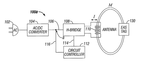
[0029] FIG. la illustrates a block diagram of an H-bridge acoustomagnetic
deactivator
that is powered by AC in accordance with one embodiment of the
present.disclosure;
[0030] FIG. lb illustrates a block diagram of an H-bridge acoustomagnetic
deactivator
which is powered by high voltage DC in accordance with an alternate embodiment
of the
present disclosure;
[0031] FIG. 1 c illustrates a block diagram of an H-bridge acoustomagnetic
deactivator
which is powered by low voltage DC in accordance with an alternate embodiment
of the
present disclosure;
[0032] FIG. 2a illustrates a circuit diagram of the H-bridge circuit of FIG.
la which is
powered by AC in accordance with an alternate embodiment of the present
disclosure;
[0033] FIG. 2b illustrates a circuit diagram of the H-bridge circuit of FIG.
lb which is
powered by high voltage DC in accordance with an alternate embodiment of the
present
disclosure;
[0034] FIG. 2c illustrates a circuit diagram of the H-bridge circuit of FIG.
2c which is
powered by DC in accordance with an alternate embodiment of the present
disclosure;
[0035] FIG. 3 illustrates a graph of the alternating antenna deactivation
current as a
function of time in accordance with an alternate embodiment of the present
disclosure;
[0036] FIG. 4 illustrates an equivalent circuit diagram of the H-bridge
circuit of FIGS.
2a, 2b and 2c illustrating the equivalent circuit configuration to provide
positive charging
current as a function of time;
[0037] FIG. 5 illustrates an equivalent circuit diagram of the H-bridge
circuit of FIGS.
2a, 2b and 2c illustrating the equivalent circuit configuration to provide
positive
discharging current as a function of time;
7
CA 02587871 2007-05-17
WO 2006/057887 PCT/US2005/041678
[0038] FIG. 6 illustrates an equivalent circuit diagram of the H-bridge
circuit of FIGS.
2a, 2b and 2c illustrating the equivalent circuit configuration to provide
negative charging
current as a function of time;
[0039] FIG. 7 illustrates an equivalent circuit diagram of the H-bridge
circuit of FIGS.
2a, 2b and 2c illustrating the equivalent circuit configuration to provide
negative
discharging current as a function of time;
[0040] FIG. 8a illustrates a graph of ampere-turns versus the number of tarns
for
#13AWG wire to generate activation, deactivation or reactivation energy for
various
circuit topologies in accordance with one embodiment of the present
disclosure;
[0041] FIG. 8b illustrates a graph of anlpere-turns versus the number of turns
for
#16AWG wire to generate activation, deactivation or reactivation energy for
various
circuit topologies;
[0042] FIG. 8c illustrates a graph of ampere-turns versus the number of turns
for
#2AWG wire to generate activation, deactivation or reactivation energy for
various circuit
topologies;
[0043] FIG. 9 illustrates a graph of ON charging time versus current for the H-
bridge
circuit of FIGS. 2a, 2b and 2c in accordance with one embodiment of the
present
disclosure; and
[0044] FIG. 10 illustrates an enlarged view of the graph of ON charging time
versus
current for the H-bridge circuit of FIG. 9 in accordance with one embodiment
of the
present disclosure.
DETAILED DESCRIPTION
[0045] The following co-pending, commonly owned U.S. non-provisional patent
applications are hereby incorporated by reference in their entirety:
Application No.
10/688,822 filed on October 17, 2003, entitled "Electronic Article
Surveillance Marker
Deactivator Using Phase Control Deactivation"; and Application No. 10/915,844
filed on
August 11, 2004, entitled "Deactivator Using Inductive Charging"; and commonly
owned
U.S. Patent No. 6,946,962, issued on September 20, 2005, entitled "Electronic
Article
Surveillance Marker Deactivator Using Inductive Discharge".
[0046] Numerous specific details may be set forth herein to provide a thorough
understanding of the embodiments of the disclosure. It will be understood by
those
skilled in the art, however, that various embodiments of the disclosure may be
practiced
without these specific details. In other instances, well-known methods,
procedures,
8
CA 02587871 2007-05-17
WO 2006/057887 PCT/US2005/041678
components and circuits have not been described in detail so as not to obscure
the various
embodiments of the disclosure. It can be appreciated that the specific
structural and
functional details disclosed herein are representative and do not necessarily
limit the
scope of the disclosure.
[0047] It is worthy to note that any reference in the specification to "one
embodiment"
or "an embodiment" according to the present disclosure means that a particular
feature,
stracture, or characteristic described in connection with the embodiment is
included in at
least one embodiment. The appearances of the phrase "in one embodiment" in
various
places in the specification are not necessarily all referring to the same
embodiment.
[0048] Some embodiments may be described using the expression "coupled" and
"connected" along with their derivatives. For example, some embodiments may be
described using the term "connected" to indicate that two or more elements are
in direct
physical or electrical contact with each other. In another example, some
embodiments
may be described using the term "coupled" to indicate that two or more
elements are in
direct physical or electrical contact. The term "coupled," however, may also
mean that
two or more elements are not in direct contact with each other, but yet still
co-operate or
interact with each other. The embodiments are not limited in this context.
[0049] Referring now in detail to the drawings wherein like parts may be
designated by
like reference numerals throughout, the main components of an H-bridge
deactivator are
shown in FIGS. la-c for different input power conditioning. FIG. la
illustrates a block
diagram of an H-bridge acoustomagnetic deactivator 100a that is powered by AC
in
accordance with one embodiment of the present disclosure. Deactivator 100a may
be
configured to include a number of different elements or additional elements
may be added
to deactivator 100a, or be substituted for the representative elements shown
in FIG. 1 a,
and those elements still fall within the scope of the embodiments described
herein.
[0050] Specifically, AC input voltage source 102 provides current and is
coupled to
AC/DC converter 104. Typically, the AC input voltage may range from about 110
to
about 120 VAC or from about 220 to about 240 VAC. AC/DC converter 104
transmits
power to H-bridge 108 via line 106. Antenna 110 receives from the H-bridge 108
alternating and decaying currents "I" required to generate magnetic field "M"
for
deactivation of EAS tag 130. Alternatively, the constantly positive or
constantly negative
currents "I" can be applied to activate or reactivate EAS tag 130. A circuit
controller
section 112 controls activation, deactivation or reactivation timing of the H-
bridge circuit
108. The circuit controller section 112 receives feedback from the H-bridge
108 via line
9
CA 02587871 2007-05-17
WO 2006/057887 PCT/US2005/041678
114 and transmits a feedback signal via line 116 to the input of the H-bridge
108 at
junction "a" with line 106.
[0051] FIG. lb illustrates a block diagram of an H-bridge acoustomagnetic
deactivator
100b that is powered by high voltage DC in accordance with one embodiment.
Similar to
deactivator 100a, deactivator 100b may include a number of different elements.
In
particular, the H-bridge deactivator circuit 108 and associated components
antenna 110,
circuit controller section 112 and EAS tag 130 illustrated in FIG. lb are
identical to those
illustrated in FIG. 1 a, with the exception that DC/DC high voltage converter
120 is
connected via line 106 upstream of junction "a" and connected to AC/DC
converter 104
via line 122. Therefore, the DC output voltage of AC/DC converter 104 is
increased by a
DC/DC high voltage converter 120 (or in other ways known in the art) to supply
high
voltage DC to H-bridge circuit 108.
[0052] FIG. lc illustrates a block diagram of an H-bridge acoustomagnetic
deactivator
100c that is powered by DC in accordance with one embodiment. As with respect
to FIG.
lb, the H-bridge deactivator circuit 108 and associated components antenna
110, control
section 112 and EAS tag 130 illustrated in FIG. 1 c are identical to those
illustrated in
FIG. 1a, with the exception that DC battery 124 is connected via line 106 at
junction "b"
which is upstream of junction "a" and connected to AC/DC charger 124. Battery
124 is a
standard 12V or 24V car, boat, or small plane battery that provides energy
storage
capability and can be the main power supply input to H-bridge circuit 108.
Typically,
battery 124 has a high cold cranking current capacity in the range of 600 amps
and an
amp-hour rating in the range of 100 amp-hours.
[0053] FIGS. 2a to 2c illustrate an H-bridge circuit 108 which includes four
switches
SW1, SW2, SW3 and SW4 which are joined at junctions 1, 2, 3 and 4 to form a
bridge.
In particular, FIG. 2a illustrates a circuit diagram of the H-bridge circuit
108 of FIG. 1 a
that is powered by AC in accordance with one embodiment. Specifically, first
switch
SW1 is coupled to first junction 1 and to third junction 3, second switch SW2
is coupled
to second junction 2 and to fourth junction 4, third switch SW3 is coupled to
first junction
1 and to fourth junction 4, and fourth switch SW4 is coupled to third junction
3 and to
second junction 2. First end 110a of coil antenna 110 is coupled to third
junction 3 and
second end 110b of coil antenna 110 is coupled to fourth junction 4. Thus, the
first
switch SWl, coupled to first junction 1 and to third junction 3, and third
switch SW3,
coupled to first junction 1 and to fourth junction 4, form a triangle with
coil antenna 110.
Similarly, the second switch SW2, coupled to second junction 2 and fourth
junction 4,
CA 02587871 2007-05-17
WO 2006/057887 PCT/US2005/041678
and fourth switch SW4, coupled to second junction 2 and third junction 3, also
form a
triangle with coil antenna 110. Thus, the first switch SW1 controls current
between the
first junction 1 and the third junction 3. The second switch SW2 controls
current between
the second junction 2 and the fourth junction 4. The third switch SW3 controls
current
between the first junction 1 and the fourth junction 4. The fourth switch SW4
controls
current between the second junction 2 and the third junction 3. The switches
SW1, SW2,
SW3 and SW4 include high current transistors which produce currents "I" and,
correspondingly, magnetic fields "M" from coil antenna 110 of sufficient
magnitude to
activate, deactivate or reactivate the EAS tag 130. AC voltage source 102 is
coupled in
series with rectifier 204a to junction 1 of the H-bridge circuit 108 through
junction "c"
and to junction 2 of the H-bridge circuit 108 through junction "d". Through
junction "a",
capacitor 204b is coupled to the H-bridge circuit 108 through junction 1 and,
through
junction "d", coupled to junction 2 of the H-bridge circuit 108. Consequently,
the AC
voltage source 102 and rectifier 204a are also coupled in parallel with
capacitor 204b via
junction "a" and junction "d". Therefore, AC voltage from the AC voltage
source 102 is
converted via rectifier 204a and capacitor 204b to DC and coupled to the H-
bridge circuit
108 through junctions 1, 2, 3 and 4.
[0054] FIG. 2b illustrates a circuit diagram of the H-bridge circuit 108 of
FIG. lb that
is powered by high voltage DC in accordance with one embodiment. In
particular, the H-
bridge deactivator circuit 108 and associated rectifier 204a, capacitor 204b,
SW1, SW2,
SW3, SW4 and antenna 110 are identical to those illustrated in FIG. 2a, with
the
exception that DC/DC high voltage converter 120 is connected upstream of
junction "a".
Consequently, high voltage DC is supplied to the H-bridge circuit 108 through
junctions
1,2,3and4.
[0055] FIG. 2c illustrates a circuit diagram of the H-bridge circuit 108 of
FIG. 1 c that
is powered by DC in accordance with one embodiment. In particular, the H-
bridge
deactivator circuit 108 and associated antenna 110 and SW1, SW2, SW3 and SW4
are
identical to those illustrated in FIG. 2a, with the exception that DC battery
124 is
connected at junctions "c" and "d" to supply DC power to the H-bridge
deactivator 108
through junctions 1, 2, 3 and 4.
[0056] FIG. 3 illustrates a graph of the alternating antenna activation,
deactivation or
reactivation current as a function of time in accordance with one embodiment.
Specifically, the current "I" is plotted as a function of time "t". During
Switch "ON"
times Tl, T2, T3 and T4, positive charging currents 301a, 302a, 303a and 304a
are
11
CA 02587871 2007-05-17
WO 2006/057887 PCT/US2005/041678
,. .,,.... _ .. . ,.
generated. The positive charging currents 301a, 302a, 303a and 304a are
followed by
positive discharging currents 301b, 302b, 303b and 304b during which time the
current
"I" decays to zero. By reversing direction of current flow through the coil
antenna 110,
and again supplying power, negative charging currents 301 c, 302c, 303c and
304c are
generated. These negative charging currents 301c, 302c, 303c and 304c are
followed by
negative discharging currents 301d, 302d, 303d and 304d, during which time,
the current
"I" again decays to zero. As a result, with respect to FIGS. 2a to 2c, by
alternating and
adjusting the switch on times Tl', T2', T3' and T4' of switches SW1, SW2, SW3
and
SW4, an alternating and decaying current "I" can be generated through the coil
antenna
110 for deactivation or a constant polarity positive magnetic field or a
constant polarity
negative magnetic field can be generated for activation or reactivation
through the coil
antenna 110.
[0057] In particular, following connection of the source of DC power, such as
AC/DC
converter 104, DC/DC High Voltage converter 120, battery 124 or AC/DC charger
126,
between the first and second junctions 1 and 2, respectively, to apply current
to the circuit
108, the circuit 108 generates in a first cycle Cl a positive increasing
magnetic field from
the antenna 110 by virtue of the circuit controller 112 opening the third
switch SW3;
opening the fourth switch SW4; closing the first switch SW1 to direct current
"I" from
the first junction 1 to the third junction 3; and closing the second switch
SW2 to direct
current "I" from the fourth junction 4 to the second junction 2, thereby
directing an
increasing current 301a through the antenna 110 in a first direction from the
third junction
3 to the fourth junction 4.
[0058] The circuit controller 112 further generates in the first cycle C 1 a
positive
decreasing magnetic field from the antenna 110 by disconnecting the source of
DC
power, (e.g., AC/DC converter 104, DC/DC High Voltage converter 120, battery
124 or
AC/DC charger 126) between the first and second junctions 1 and 2,
respectively;
opening the first switch SW1; opening the third switch SW3; opening the fourth
switch
SW4; and closing the second switch SW2, thereby directing a decreasing current
301b
through the antenna 110 in a first direction from the third junction 3 to the
fourth junction
4.
[0059] The circuit controller 112 continues to generate in the first cycle C1
a negative
increasing magnetic field from the antenna 110 by connecting a source of DC
power (e.g.,
AC/DC converter 104, DC/DC High Voltage converter 120, battery 124 or AC/DC
charger 126) between the first and second junctions, 1 and 2, respectively;
opening the
12
CA 02587871 2007-05-17
WO 2006/057887 PCT/US2005/041678
first switch SW1; opening the second switch SW2; closing the third switch SW3
to direct
the current "I" from the first junction 1 to the fourth junction 4; and
closing the fourth
switch SW4 to reverse current flow through the antenna 10 by directing the
current "I"
from the third junction 1 to the second junetion 2, thereby directing
increasing current
301c through the antenna 110 in a second direction from the fourth junction 4
to the third
junction 3 which is a direction reverse to the first direction.
[0060] In the first cycle, the circuit controller 112 is also configured to
generate a
negative decreasing magnetic field from the antenna 110 by disconnecting the
source of
DC power (i.e., an AC/DC converter 104, DC/DC High Voltage converter 120,
battery
124 or AC/DC charger 126) between the first and second junctions, 1 and 2,
respectively;
opening the first switch SW1; opening the second switch SW2; opening the third
switch
SW3; and closing the fourth switch SW4, thereby directing decreasing current
301d
through the antenna 110 in a second direction from the fourth junction 4 to
the third
junction 3.
[0061] In a second cycle C2 and succeeding cycles such as C3 and C4, following
connection of the source of DC power between the first and second junctions,
the circuit
generates from the antenna 110 in the second and succeeding cycles C2 through
C4
initially a positive increasing magnetic field, followed by positive
decreasing magnetic
field, a negative increasing magnetic field, and a negative decreasing
magnetic field, by
virtue of the circuit controller 112 repeating the same steps as disclosed
above for the first
cycle Cl. Due to the magnitude of the currents 301 a to 301 d being greater
than the
magnitude of the currents 302a to 302d, and, in turn, the magnitude of the
currents 302a
to 302d being greater than the magnitude of the currents 303a to 303d and, in
turn, the
magnitude of the currents 303a to 303d being greater than the magnitude of the
currents
304a to 304d, cycle time of the first cycle Cl exceeds cycle time of the
second cycle C2,
and cycle time of each succeeding cycle, such as cycles C3 and C4,
consecutively
decreases with respect to the cycle time of the second cycle C2.
[0062] As a result, the alternating current "I" can be designed to activate,
deactivate or
reactivate an AM label. It should be noted that while four positive charging
Switch "ON"
times T1, T2, T3 and T4 and four cycles C1 through C4 are illustrated in FIG.
3, those
skilled in the art recognize that any number of Switch "ON" times, either
greater than or
less than four, and any number of cycles can be generated as required or
preferred to
activate, deactivate or reactivate a particular acoustomagnetic (AM) label.
13
CA 02587871 2007-05-17
WO 2006/057887 PCT/US2005/041678
[0063] The equations (1) and (2) for the current waveforms are as follows:
I = {V/R} [1- e{"v(vx)}] (1)
Equation (1) is the equation for charging the circuit.
I = {V/R}e -'/ (''/R) (2)
Equation (2) is the equation for discharging the circuit, where for both
Equations (1) and
(2):
I = Current in amps (A)
V= Battery voltage (12 or 24VDC)
R= Antenna resistance in ohms (SZ)
e= Natural number'2.71828
L= Antenna inductance in henrys (H)
t=time in seconds (s)
[0064] As noted previously, the battery 124 is typically a standard car, boat
or small
plane battery with high cold cranking amps (N600) and a high amp-hour rating (-
100).
The antenna 110 is made from large gauge cable to minimize losses, wrapped "N"
times
in a loop of arbitrary shape, usually circular or square. This multiple
looping around an
area creates an inductance "L" and a resistance "R". The losses are
proportional to the
resistance "R". The rate of rise of the charge current "I" and the rate of
discharge of that
current "I" is proportional to the ratio of L/R. The ratio L/R is known as the
time
constant "ti".
The antenna resistance R is given by Equation (3) as follows:
R = p len (3)
where len = length of the cable, and the length of the cable, len, is given by
Equation (4),
as follows:
14
CA 02587871 2007-05-17
WO 2006/057887 PCT/US2005/041678
len = N C (4)
where C = circumference for a circular loop antenna is given by Equation (5),
as
follows:
C = 7c D (5)
D= diameter of circle, and
N= number of turns or wraps of the antenna cable.
Then, for a circular antenna, the resistance R is given by Equation (6), as
follows:
R=pN7c/D (6)
The antenna inductance L is given by Equation (7), as follows:
L= Nz A/ len (7)
where
= permeability of free space, i.e.,
=4x10"7 H/m
N = number of turns in the antenna, and
A= area of loop in the antenna.
CA 02587871 2007-05-17
WO 2006/057887 PCT/US2005/041678
The area of loop in the antenna is given by Equation (8), as follows:
A =,gD2/4 (8)
for a circular antenna.
[0065] FIG. 4 illustrates an equivalent circuit diagram of the H-bridge
circuit of FIGS.
2a, 2b and 2c illustrating the equivalent circuit configuration to provide
positive charging
current "I" as a function of time "t" in accordance with one embodiment.
Specifically,
the positive charging currents 301a, 3 02a, 303a and 304a of FIG. 3 are
generated through
coil antenna 110 as illustrated in FIG. 4 by closing SW1 and SW2, with SW3 and
SW4
being open, for the charge time T1, T2, T3 and T4. Equation (1) provides the
calculation
for the charging current "I".
[0066] FIG. 5 illustrates an equivalent circuit diagram of the H-bridge
circuit of FIGS.
2a, 2b and 2c illustrating the equivalent circuit configuration to provide
positive
discharging current "I" as a function of time "t" in accordance with one
embodiment.
Specifically, the positive discharging currents 301b, 302b, 303b and 304b of
FIG. 3 are
generated through coil antenna 110 as illustrated in FIG. 5 by closing SW2,
with SW 1,
SW3, and SW4 being open, for the discharge time. Equation (2) provides the
calculation
for the discharging current "I".
[0067] FIG. 6 illustrates an equivalent circuit diagram of the H-bridge
circuit of FIGS.
2a, 2b and 2c illustrating the equivalent circuit configuration to provide
negative charging
current "I" as a function of time "t" in accordance with one embodiment.
Specifically,
the negative charging currents 301c, 3 02c, 303c and 3 04c of FIG. 3 are
generated through
coil antenna 110 as illustrated in FIG. 6 by closing SW3 and SW4, with SW1 and
SW2
being open for the charge time. The negative charging currents are generated
by
increasing current through the coil antenna 110 with the currents 301c, 302c,
303c and
304c being in the direction opposite to that of the positive charging currents
301a, 302a,
303a and 304a illustrated in FIG. 4. Again, Equation (1) provides the
calculation for the
charging current "I".
[0068] FIG. 7 illustrates an equivalent circuit diagram of the H-bridge
circuit of FIGS.
2a, 2b and 2c illustrating the equivalent circuit configuration to provide
negative
discharging current "I" as a function of time in accordance with one
embodiment.
Specifically, the negative discharging currents 301d, 302d, 303d and 304d of
FIG. 3 are
16
CA 02587871 2007-05-17
WO 2006/057887 PCT/US2005/041678
generated through coil antenna 110 as illustrated in FIG. 7 by closing SW4,
with SW1,
SW2, and SW3 being open for the discharge time. Again, Equation (2) provides
the
calculation for the discharging current "I".
[0069] Decaying amplitude pulses, i.e. discharging currents, are calculated by
solving
Equations (1) and (2) for time "t" at a desired current "I".
[0070] Since the Amp-Turns product (AT) is a measure of the magnetic field
strength
of the activator, deactivator or reactivator, the activation, deactivation or
reactivation
energy is a function of the number of turns required to generate the magnetic
field
strength required to deactivate an EAS tag. AT is the product of the number of
turns (N)
times the peak current (I). An AT product of 10000-15000 is comparable to
existing
deactivators of similar size. Since I = V/R, the product AT is calculated by
first
determining the resistance R as a function of the number of turns N, as given
by Equation
(9), as follows:
R(N)=pN7c +0.01 (9)
where .01 is the resistance in ohms (SZ) of two power field effect transistors
(FETs) and p
is the electrical resistivity of the metal conductor cable in ohm/ft. FETs
when in the ON
position are high current transistors and when in the OFF position are high
impedance
transistors.
[0071] The action state of each of the switches in their ON and OFF positions
is
disclosed in the following table:
ACTION SWl SW2 SW3 SW4
STATE
Positive ON ON OFF OFF
Charging
301a, 302a,
303a,304a
Positive OFF ON OFF OFF
Discharging
301b, 302b,
303b, 304b
17
CA 02587871 2007-05-17
WO 2006/057887 PCT/US2005/041678
Negative OFF OFF ON ON
Charging
301c, 302c,
303c, 304c
Negative OFF OFF OFF ON
Discharging
301d, 302d,
303d, 304d
[0072] An acoustomagnetic EAS tag such as EAS tag 130 can be activated or
reactivated by coupling to just the positive charging magnetic fields 301 a,
302a, 303a,
304a and to the positive discharging magnetic fields 301b, 302b, 303b, 304b or
by
coupling to just the negative charging magnetic fields 301c, 302c, 303c, 304c
and to the
negative discharging magnetic fields 301d, 302d, 303d, 304d, but not to an
alternating
magnetic field which varies from positive to negative or from negative to
positive. As a
result, it is contemplated that the H-bridge circuit 108 is not only a
deactivator circuit but
also an activator or a reactivator circuit.
[0073] A method of activating or reactivating the electronic article
surveillance (EAS)
tag 130 includes the steps of: providing the H-bridge circuit 108 coupled to
the antenna
110; applying a source of current I to the H-bridge circuit 108; directing an
increasing
current flow I through the antenna 110 in a defined direction, thereby
generating an
increasing magnetic field M from the antenna 110; and directing a decreasing
current
flow I through the antenna 110 in the defined direction, thereby generating a
decreasing
magnetic field M from the antenna 110. In one particularly useful embodiment,
the
defined direction is a first direction such that the increasing magnetic field
M is a positive
increasing magnetic field and the decreasing magnetic field M is a positive
decreasing
magnetic field M. In one particularly useful embodiment, the defined direction
is a
second direction reverse to the first direction such that the increasing
magnetic field M is
a negative increasing magnetic field and the decreasing magnetic field M is a
negative
decreasing magnetic field M.
[0074] More particularly, referring to FIGS. 4 and 5, coupling of EAS tag 130
to just
the positive charging magnetic fields 301a, 302a, 303a, 304a and to the
positive
discharging magnetic fields 301b, 302b, 303b, 304b can be effected, as
previously
18
CA 02587871 2007-05-17
WO 2006/057887 PCT/US2005/041678
discussed, by operating only switches SW1 and SW2. Switches SW1, SW2, SW3 and
SW4 each include a bypass diode dl, d2, d3 and d4, respectively, which
bypasses the
switch to allow current decay in the normal direction of current flow through
the
respective switch upon closure of the switch while disallowing current flow in
the reverse
direction. Therefore, although reactivation requires direct operation of only
switches
SWl and SW2, decay current flow still occurs through diode 0 or d4, depending
upon
the original circuit configuration, even though switches SW3 and SW4 remain
closed, so
that three switches are required for reactivation, i.e., SW1, SW2 and SW3 or
SW1, SW2
and SW4.
[0075] Similarly, referring to FIGS. 6 and 7, coupling of EAS tag 130 to just
the
negative charging magnetic fields 301c, 302c, 303c, 304c and to the negative
discharging
magnetic fields 301d, 302d, 303d, 304d can be effected, as previously
discussed, by
operating only switches SW3 and SW4. Again, although reactivation requires
direct
operation of only switches SW3 and SW4, decay current flow still occurs
through diode
dl or d2, depending upon the original circuit configuration, even though
switches SW1
and SW2 remain closed, so that three switches are required for reactivation,
i.e., SW3,
SW4 and SW1 or SW3, SW4 and SW2.
[0076] In view of Equation (9) for the resistance R(N), then the current "I"
as a
function of N is calculated by Equation (10), as follows:
I(N) = V/R(N) (10)
where V=1 lOVDC for AC/DC applications, or V> 110VDC for DC/DC high voltage
application or V= 12VDC or 24VDC for battery application.
[0077] The number of ampere-turns AT or NI (N) as a function of the number of
turns
N is given by Equation (11), as follows:
NI(N) = N-I(N) (11)
[0078] FIGS. 8a-c shows the number of turns required to generate activation,
deactivation or reactivation energy for various circuit topologies. In
particular, FIG. 8a
illustrates a graph of ampere-turns AT or NI(N) versus the number of turns N
for
19
CA 02587871 2007-05-17
WO 2006/057887 PCT/US2005/041678
#13AWG wire to generate activation, deactivation or reactivation energy for
various
circuit topologies in accordance with one embodiment. In FIG. 8a, the
resistivity of the
wire is p = 2003. 10"6 S2/ ft. For an AC/DC application such as is illustrated
in FIG. 1 a,
V=110VDC. Notice that at N=10, the AT is about 15000.
[0079] FIG. 8b illustrates a graph of ampere-turns AT or NI(N) versus the
number of
turns N for #1 6AWG wire to generate activation, deactivation or reactivation
energy for
various circuit topologies in accordance with one embodiment. In FIG. 8b, the
resistivity
of the wire is p = 4016= 10-6 SZ/ ft. For a DC/DC high voltage application
such as is
illustrated in FIG. lb, V=200VDC. Notice that atN=14, the AT is about 15000.
[0080] FIG. 8c illustrates a graph of ampere-turns AT or NI(N) versus the
number of
turns N for #2AWG wire to generate activation, deactivation or reactivation
energy for
various circuit topologies in accordance with one embodiment. In FIG. 8c, the
resistivity
of the wire is 156= 10"6 SZ/ ft. For a battery application such as is
illustrated in FIG. 1 c, V=
12VDC. Notice that at N=30, the AT is about 15000.
[0081] For each instance illustrated in FIGS. 8a to 8c, the wire gauge can
vary as
smaller diameter wire can be used in higher voltage topologies.
[0082] With respect to the frequency of activation, deactivation or
reactivation, the
activation, deactivation or reactivation frequency increases as the current
activation,
deactivation or reactivation waveform decays because, as can be seen from FIG.
3, the
interval between Switch "ON" times Tl, T2, T3 and T4 decreases. That is, the
positive
and negative charging currents "I" are shut off earlier and earlier,
corresponding to an
increase in the deactivation frequency. The "ON" time of the switches SW 1,
SW2, SW3
and SW4, which are comprised of FETs, is calculated by solving Equations 1 and
2 for
time "t".
[0083] A solution for charging time "t" is shown in Equation (12), as follows:
t(I) = -ti{ l - (IR)/V} (12)
[0084] FIG. 9 illustrates a graph of "ON" charging time "t" versus current "I"
for the
H-bridge circuit of FIGS. 2a, 2b and 2c in accordance with one embodiment.
FIG. 10
illustrates an enlarged view of the graph of "ON" charging time versus current
for the H-
bridge circuit of FIG. 9 in accordance with one embodiment.
CA 02587871 2007-05-17
WO 2006/057887 PCT/US2005/041678
[0085] A solution for discharging time "t" is shown in Equation (13), as
follows:
t(I) = -i{(IR)/V} (13)
[0086] Those skilled in the art recognize that plots of discharge time "t"
versus current
"I" can be computed and plotted in a similar manner to the charge time "t"
based on
Equation (12) and the graphs of FIG. 9 and FIG. 10.
[0087] Based on the foregoing, and referring to FIGS. la-1c, 2a-2c, and 3-7,
it can be
understood that a method is disclosed for activating or deactivating or
reactivating an
EAS tag 130 which includes the steps of: providing an H-bridge circuit 108
coupled to an
antenna 110; applying a source of current via line 106 to the H-bridge circuit
108; and
directing an increasing current flow I through the antenna 110 in a first
direction, thereby
generating a positive increasing magnetic field M from the antenna, or
directing a
decreasing current flow I through the antenna 110 in the first direction,
thereby generating
a positive decreasing magnetic field M from the antenna 110; directing an
increasing
current flow I through the antenna 110 in a second direction such that
direction of current
flow I through the antenna 110 is in a direction reverse to that of direction
of current flow
I in the first direction, thereby generating a negative increasing magnetic
field M from the
antenna 110, or directing a decreasing current flow I through the antenna 110
in the
second direction, thereby generating a negative decreasing magnetic field M
from the
antenna 110.
[0088] The method may be implemented such that the antenna 110 includes first
and
second ends for directing current I through the antenna 110 and the H-bridge
circuit 108
includes first, second, third and fourth switches SW1, SW2, SW3 and SW4,
respectively.
The first and third switches SW1 and SW3 may be coupled to a first junction 1;
the
second and fourth switches SW2 and SW4 may be coupled to a second junction 2;
the
first and the fourth switches SW1 and SW4 may be coupled to a third junction
3; and the
third switch SW3 and the second switch SW2 may be coupled to a fourth junction
4. The
first end 110a of the antenna 110 may be coupled to the third junction 3 and
the second
end 110b of the antenna 110 may be coupled to the fourth junction 4. The first
switch
SW1 may control current I between the first junction 1 and the third junction
3; the
second switch SW2 may control current I between the second junction 2 and the
fourth
junction 4; the third switch SW3 may control current I between the first
junction 1 and the
21
CA 02587871 2007-05-17
WO 2006/057887 PCT/US2005/041678
fourth junction 4; and the fourth switch SW4 may control current I between the
second
junction 2 and the third junction 3.
[0089] The method may further be implemented such that the step of directing
an
increasing current flow I through the antenna 110 in a first direction is
performed by:
connecting the current source via line 106 between the first and second
junctions, 1 and 2;
opening the third and fourth switches, SW3 and SW4, closing the first switch
SW1 to
direct current I from the first junction 1 to the third junction 3; and
closing the second
switch SW2 to direct current I from the fourth junction 4 to the second
junction 2, thereby
directing from the third junction 3 to the fourth junction 4 an increasing
current I through
the antenna 110 in the first direction to generate the positive increasing
magnetic field M.
[00901 The method may further be implemented such that the step of directing a
decreasing current flow I through the antenna 110 in a first direction is
performed by:
disconnecting the current source via line 106 between the first and second
junotions 1 and
2; opening the first, third and fourth switches SW1, SW3 and SW4; and closing
the
second switch SW2, thereby directing a decreasing current I through the
antenna 110 in
the first direction from the third junction 3 to the fourth junction 4 to
generate the positive
decreasing magnetic field M.
[0091] The method may further be implemented such that the step of directing
an
increasing current flow I through the antenna 110 in a second direction is
performed by:
connecting the current source via line 106 between the first and second
junctions 1 and 2;
opening the first and second switches SW1 and SW2; closing the third switch
SW3 to
direct current I from the first junction 1 to the fourth junction 4; and
closing the fourth
switch SW4 to direct current I from the third junction 3 to the second
junction 2, thereby
directing from the fourth 4 junction to the third junction 3 increasing
current I through the
antenna 110 in a second direction to generate the negative increasing magnetic
field M.
[0092] The method may further be implemented such that the step of directing a
decreasing current flow tlirough the antenna in the second direction is
performed by:
disconnecting the current source between the first and second junctions;
opening the first,
second and third switches; and closing the fourth switch, thereby directing
decreasing
current through the antenna in the second direction from the fourth junction
to the third
junction to generate the negative decreasing magnetic field.
[0093] As a result of the foregoing, the present disclosure provides an
alternate method
for activation, deactivation or reactivation of an EAS acoustomagnetically
activated tag
by utilizing an H-bridge circuit to generate the alternating and decaying
currents required
22
CA 02587871 2007-05-17
WO 2006/057887 PCT/US2005/041678
for activation, deactivation or reactivation. The present disclosure enables
low voltage
activation, deactivation or reactivation of an EAS tag, e.g., at voltage
levels of 12 to
24VDC, and ensures uninterruptible power for activation, deactivation or
reactivation of
an EAS tag in case of external power loss.
[0094] The present disclosure provides a portable apparatus for activation,
deactivation
or reactivation of an EAS tag and the activation, deactivation or reactivation
can be
performed without a high voltage capacitor that is required typically in large
deactivation
designs. The present disclosure provides alternate methods of activation,
deactivation or
reactivation so that a designer may optimize for a particular environment.
[0095] Some embodiments may be implemented using an architecture that may vary
in
accordance with any number of factors, such as desired computational rate,
power levels,
heat tolerances, processing cycle budget, input data rates, output data rates,
memory
resources, data bus speeds and other performance constraints. For example, an
embodiment may be implemented using software executed by a general-purpose or
special-purpose processor. In another example, an embodiment may be
implemented as
dedicated hardware, such as a circuit, an application specific integrated
circuit (ASIC),
progrannnable logic device (PLD) or digital signal processor (DSP), and so
forth. In yet
another example, an embodiment may be implemented by any combination of
programmed general-purpose computer components and custom liardware
components.
The embodiments are not limited in this context.
[0096] While certain features of the embodiments of the invention have been
illustrated
as described herein, many modifications, substitutions, changes and
equivalents will now
occur to those skilled in the art. It is, therefore, to be understood that the
appended claims
are intended to cover all such modifications and changes as fall within the
true spirit of
the embodiments of the invention.
23