Note : Les descriptions sont présentées dans la langue officielle dans laquelle elles ont été soumises.
CA 02590147 2007-06-08
1
[DOCUMENT] SPECIFICATION
[TITLE OF THE INVENTION] BIDIRECTIONAL FIELD-EFFECT
TPANSISTOR AND MATRIX CONVERTER
[TECHNICAL FIELD]
[0001]
The present invention relates to bidirectional field-
effect transistors, which can control a current flowing bi-
directionally, and a matrix converter using the transistors.
[BACKGROUND]
[0002]
Fig. 7a is a circuit diagram showing an example of a
conventional matrix converter. Figs. 7b to 7d are circuit
diagrams of switching devices. The matrix converter CV has
function of converting an AC (alternating current) power
having a frequency to another AC power having a different
frequency.
[0003]
A three-phase AC power source PS supplies a three-
phase AC power having a frequency Fa through three lines R,
S and T. A three-phase AC motor M is driven by another
three-phase AC power having another frequency Fb, which is
supplied through three lines U, V and W.
[0004]
The matrix converter CV includes the input lines R, S
and T, the output lines U, V and W, and nine switching
CA 02590147 2007-06-08
2
devices SW, which are arranged in matrix between the
respective lines R, S and T and the respective lines U, V
and W, for controlling opening and closing between the
mutual lines. Each of the switching devices SW is driven
by a control circuit (not shown) which can operate PWM
(pulse width modulation) with desired timings.
[0005]
Since each of the switching devices SW must open and
close the AC current flowing forward and backward, a common
power transistor cannot perform this operation. Hence,
certain ingenuity of circuit arrangement is required.
[0006]
In the conventional matrix converter, as shown in Fig.
7c, a first series circuit having an IGBT (Insulated Gate
Bipolar Transistor) device Ql and a diode device Dl, and a
second series circuit having an IGBT device Q2 and a diode
device D2 are connected in anti-parallel with each other,
to constitute a single switching device SW. Since IGBT
devices can control only one-way current, such anti-
parallel connection can control the bidirectional current.
In addition, IGBT devices have a low reverse blocking
voltage, therefore, the reverse blocking voltage can be
improved by using the series-connected diode device.
[0007]
In the above-described circuitry, however, four power
CA 02590147 2007-06-08
3
device are needed to constitute the single switching device
SW. In the case of three-phase to three-phase conversion
shown in Fig. 7a, thirty-six power devices are needed to
constitute the nine switching device SW. Further, each
power device must have larger ratings of voltage and
current, thereby resulting in larger scale of circuitry and
a larger cooling mechanism for dissipating a great deal of
heat.
[0008]
In order to solve these problems, RB(Reverse
Blocking)-IGBT devices, as shown in Fig. 7d, have been
proposed in the following non-patent document 1.
[0009]
[NON-PATENT DOCUMENT 1] Proceedings of 2004 International
Symposium on Power Semiconductor Devices & ICs, Kitakyushu,
pp. 121-124
[DISCLOSURE OF THE INVENTION]
[PROBLEM TO BE SOLVED BY THE INVENTION]
[0010]
The RB-IGBT device, which is integrated with a diode
area on a side of a semiconductor substrate on which an
IGBT device is formed, is equivalent in circuitry to the
series circuit having the IGBT device and the diode device
shown in Fig. 7c.
[0011]
CA 02590147 2007-06-08
4
Even in the case of using RB-IGBT devices, however,
two RB-IGBT devices must be connected in anti-parallel with
each other to control the bidirectional current. Hence,
two power devices are needed to constitute the single
switching device SW, resulting in larger scale of circuitry
and a larger cooling mechanism.
[0012]
It is an object of the present invention to provide a
bidirectional field-effect transistor, which can control a
current flowing bi-directionally by means of a single
device.
[0013]
Further, it is another object of the present invention
to provide a matrix converter with a smaller size and a
larger capacity by using the bidirectional field-effect
transistors.
[MEANS FOR SOLVING THE PROBLEM]
[0014]
In order to achieve the object, a bidirectional field-
effect transistor according to the present invention,
includes:
a semiconductor substrate;
a gate region which is formed on the semiconductor
substrate, the region including a channel parallel to a
principal surface of the substrate, and a gate electrode
CA 02590147 2007-06-08
for controlling conductance of the channel;
a first region which is provided on a first side of
the channel; and
a second region which is provided on a second side of
5 the channel;
wherein both of a first current flowing from the first
region through the channel to the second region and a
second current flowing from the second region through the
channel to the first region are controlled by a gate
voltage applied to the gate electrode.
[0015]
It is preferable in the present invention that the
gate region is arranged in the center of the first region
and the second region.
[0016]
Further, it is preferable in the present invention
that an interval between the gate electrode and a first
electrode residing in the first region is substantially
equal to another interval between the gate electrode and a
second electrode residing in the second region.
[0017]
Furthermore, it is preferable in the present invention
that an interval between the channel of the gate region and
a first contact layer residing in the first region is
substantially equal to another interval between the channel
CA 02590147 2007-06-08
6
of the gate region and a second contact layer residing in
the second region.
[0018]
Moreover, it is preferable in the present invention
that the transistor is of junction type wherein the gate
region includes a p-n junction.
[0019]
Moreover, it is preferable in the present invention
that the transistor is of MIS (Metal-Insulator-
Semiconductor) type wherein the gate region includes a
metal layer, an insulation layer and a semiconductor layer.
[0020]
Moreover, it is preferable in the present invention
that the transistor is of MES (Metal-Semiconductor) type
wherein the gate region includes a Schottky junction of a
metal and a semiconductor.
[0021]
Further, it is preferable in the present invention
that the semiconductor substrate is formed of SiC.
[0022]
A matrix converter according to the present invention,
includes:
a plurality of input lines in which alternating
currents having a first frequency flow;
a plurality of output lines in which alternating
CA 02590147 2007-06-08
7
currents having a second frequency flow;
a plurality of switching devices for controlling
opening and closing between the respective input lines and
the respective output lines;
wherein for the switching devices, the above-described
bidirectional field-effect transistors are used.
[EFFECT OF THE INVENTION]
[0023]
According to the present invention, on the
semiconductor substrate, the gate region including the
channel parallel to the principal surface of the substrate
is provided, and the first and the second regions are
provided on the first and the second sides of the channel,
respectively, thereby realizing a bidirectional field-
effect transistor which can operate both in a forward mode
where the first region acts as a source and the second
region acts as a drain, and in a backward mode where the
second region acts as a source and the first region acts as
a drain. Both the forward current and the backward current
can be controlled by the gate voltage applied to the gate
electrode. Therefore, an alternating current flowing bi-
directionally can be controlled by means of only a single
device, and such an AC switching device having a smaller
size and a larger capacity can be obtained.
[0024]
CA 02590147 2007-06-08
8
Additionally, in the matrix converter which employs
the bidirectional field-effect transistors for the
switching devices, the number of such power devices can be
remarkably reduced, thereby downsizing scale of circuitry
and cooling mechanism and simplifying them as compared to
the conventional converter.
[BRIEF DESCRIPTION OF THE DRAWINGS.)
[0025]
Fig. la is a circuit diagram showing an example of a
matrix converter according to the present invention. Figs.
lb and lc are circuit diagram showing switching devices.
Fig. 2 is a cross-sectional view showing an example of
a bidirectional field-effect transistor according to the
present invention.
Fig. 3 is a cross-sectional view showing another
example of a bidirectional field-effect transistor
according to the present invention.
Fig. 4 is a cross-sectional view showing yet another
example of a bidirectional field-effect transistor
according to the present invention.
Fig. 5 is a cross-sectional view showing yet another
example of a bidirectional field-effect transistor
according to the present invention.
Fig. 6 is a cross-sectional view showing still another
example of a bidirectional field-effect transistor
CA 02590147 2007-06-08
9
according to the present invention.
Fig. 7a is a circuit diagram showing an example of a
conventional matrix converter. Figs. 7b to 7d are circuit
diagrams of switching devices.
[EXPLANATORY NOTE]
[0026]
1 SUBSTRATE
2 BUFFER LAYER
3 CHANNEL LAYER
4 RESURF LAYER
l0a COMMON ELECTRODE
lla FIRST ELECTRODE
11, 12 N+ CONTACT LAYER
12a SECOND ELECTRODE
13 P+ LAYER
13a GATE ELECTRODE
13b FIELD PLATE
14, 16 INSULATION LAYER
15 P LAYER
CV MATRIX CONVERTER
[BEST EMBODIMENT FOR CARRYING OUT THE INVENTION]
[0027]
(First Embodiment)
Fig. la is a circuit diagram showing an example of a
CA 02590147 2007-06-08
matrix converter according to the present invention. Figs.
lb and lc are circuit diagram showing switching devices.
The matrix converter CV has function of converting an AC
power having a frequency to another AC power having a
5 different frequency. Herein, three-phase to three-phase
conversion will be exemplified. But the present invention
can be also applied to three-phase to single-phas.e
conversion, three-phase to single-phase conversion, single-
phase to three-phase conversion, single-phase to single-
10 phase conversion, as well as M-phase to N-phase conversion.
[0028]
A three-phase AC power source PS supplies a three-
phase AC power having a frequency Fa through three lines R,
S and T. A three-phase AC motor M is driven by another
three-phase AC power having another frequency Fb, which is
supplied through three lines U, V and W.
[0029]
The matrix converter CV includes the input lines R, S
and T, the output lines U, V and W, and nine switching
devices SW, which are arranged in matrix between the
respective lines R, S and T and the respective lines U, V
and W, for controlling opening and closing between the
mutual lines. Each of the switching devices SW is driven
by a control circuit (not shown) which can operate PWM
(pulse width modulation) with desired timings.
CA 02590147 2007-06-08
11
[0030]
In this embodiment, bidirectional field-effect
transistors QA as shown in Fig. lc, which can control an AC
current flowing bi-directionally by means of a single
device, are employed for these switching devices SW. Hence,
one power device is enough to constitute the one of the
single switching devices SW, so that the number of power.
devices can be remarkably reduced in the matrix converter,
thereby downsizing scale of circuitry and cooling mechanism
and simplifying them as compared to the conventional
converter.
[0031]
(Second Embodiment)
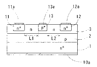
Fig. 2 is a cross-sectional view showing an example of
a bidirectional field-effect transistor according to the
present invention. Herein, a junction field-effect
transistor (J-FET) will be exemplified.
[0032]
On a substrate 1 formed is a buffer layer 2, on which
a channel layer 3 is formed. In the channel layer 3, there
are a gate region including a channel parallel to the
principal surface of the substrate 1, a first region which
is provided on a first side of the channel (left side of
the drawing), and a second region which is provided on a
second side of the channel (right side of the drawing).
CA 02590147 2007-06-08
12
[0033]
In the gate region, provided is a gate electrode 13a
for controlling conductance of the channel. In the first
region, provided is a first electrode lla which can act as
either source electrode or drain electrode. In the second
region, provided is a second electrode 12a which can act as
either drain electrode or source electrode in contrast to
the first electrode lla. Both between the gate region and
the first region and between the gate region and the second
region, formed are drift regions through which majority
carriers can pass.
[0034)
The substrate 1 can be formed of a wafer of
semiconductor, such as Si, SiC, GaN, herein, which is
formed of an n+ layer having a relatively higher carrier
concentration. On the back side of the substrate 1, formed
is a common electrode l0a which is typically grounded.
[0035J
In particular, the substrate 1 and the respective
layers 2 and 3 are preferably formed of semiconductor
material of SiC, which has excellent physical properties of
approximately three times larger energy gap, approximately
ten times higher electric breakdown field, approximately
twice higher saturation electron velocity, and
approximately three times larger thermal conductivity than
CA 02590147 2007-06-08
13
Si, thereby resulting in a power FET device with a small
size and large capacity.
[0036]
The buffer layer 2 is epitaxially grown using chemical
vapor deposition (CVD) or the like, herein, which is formed
of a p- layer having a relatively lower carrier
concentration.
[0037]
The channel layer 3 is also epitaxially grown using
chemical vapor deposition (CVD) or the like, herein, which
is formed of an n layer having a normal carrier
concentration.
[0038]
In the gate region of the channel layer 3, formed is a
p+ layer 13 having a relatively higher carrier
concentration by diffusion or ion implantation of a p-type
dopant. On the p+ layer 13, the gate electrode 13a is
formed. In the first region of the channel layer 3, formed
is an n+ contact layer 11 having a relatively higher
carrier concentration by diffusion or ion implantation of
an n-type dopant. On the n+ contact layer 11, the first
electrode lla is formed. In the second region of the
channel layer 3, formed is an n+ contact layer 12 having a
relatively higher carrier concentration by diffusion or ion
implantation of an n-type dopant. On the n+ contact layer
CA 02590147 2007-06-08
14
12, the second electrode 12a is formed.
[0039]
Next, operation of this device will be described below.
When a positive voltage +V is applied to the first
electrode 11a and a negative voltage -V is applied to the
second electrode 12a with a reference voltage (= 0 volt) of
the common electrode 10a, a forward current flows through
the path from the first electrode lla via the n+ contact
layer 11, the left drift region, the channel within the
gate region, the right drift region and the n+ contact
layer 12 to the second electrode 12a. In this state, a
negative gate voltage is applied to the gate electrode 13a,
so that a depletion layer emerges around the p-n junction
of the p+ layer 13 and the n-type channel layer 3 to
reduce conductance of the channel within the gate region,
thereby increasing resistance of the path and suppressing
the forward current.
[0040]
Meanwhile, when a negative voltage -V is applied to
the first electrode lla and a positive voltage +V is
applied to the second electrode 12a, a backward current
flows through the path from the second electrode 12a via
the n+ contact layer 12, the right drift region, the
channel within the gate region, the left drift region and
the n+ contact layer 11 to the first electrode lla. In
CA 02590147 2007-06-08
this state, a negative gate voltage is applied to the gate
electrode 13a, so that a depletion layer emerges around the
p-n junction of the p+ layer 13 and the n-type channel
layer 3 to reduce conductance of the channel within the
5 gate region, thereby increasing resistance of the path and
suppressing the backward current.
[0041]
Thus, the first and second electrodes lla and 12a can
alternately act as source electrode or drain electrode, and
10 an AC current flowing bi-directionally can be controlled by
changing the gate voltage.
[0042]
In a case of controlling an AC power as in the above-
mentioned matrix converter, it is preferable that forward
15 characteristics and backward characteristics of the
bidirectional field-effect transistor (for example, drain
current vs. drain-source voltage, drain current vs. gate-
source voltage, on-resistance, gate-source capacitance,
reverse voltage, etc) are substantially equal to each other.
[0043]
For an approach, the gate region including the gate
electrode 13a is preferably arranged in the center of the
first region including the first electrode lla and the
second region including the second electrode 12a. Thus,
the length Ll of the left drift region is equal to the
CA 02590147 2007-06-08
16
length L2 of the right drift region, thereby substantially
equalizing forward and backward characteristics with each
other.
[0044]
For another approach, an interval between the gate
electrode 13a and the first electrode lla is preferably
substantially equal to another interval between the gate
electrode 13a and the second electrode 12a, thereby
substantially equalizing forward and backward
characteristics with each other.
[0045]
For yet another approach, an interval between the
channel of the gate region and the n+ contact layer 11 is
preferably substantially equal to another interval between
the channel of the gate region and the n+ second contact
layer 12, thereby substantially equalizing forward and
backward characteristics with each other.
[0046]
For still yet another approach, the carrier
concentration of the n'' contact layer 11 is preferably
substantially equal to the carrier concentration of the n+
contact layer 12, thereby substantially equalizing forward
and backward characteristics with each other.
[0047)
For still yet another approach, a depth of the n+
CA 02590147 2007-06-08
T I
17
contact layer 11 is preferably substantially equal to a
depth of the n+ contact layer 12, thereby substantially
equalizing forward and backward characteristics with each
other.
[0048)
(Third Embodiment)
Fig. 3 is a cross-sectional view showing another
example of a bidirectional field-effect transistor
according to the present invention. Herein, a'unction
field-effect transistor (J-FET) having a RESURF (Reduced
Surface Field) layer will be exemplified.
[0049]
On a substrate 1 formed is a buffer layer 2, on which
a channel layer 3 is formed. A RESURF layer 4 is formed on
the channel layer 3. In the channel layer 3 and the RESURF
layer 4, there are a gate region including a channel
parallel to the principal surface of the substrate 1, a
first region which is provided on a first side of the
channel (left side of the drawing), and a second region
which is provided on a second side of the channel (right
side of the drawing).
[0050]
In the gate region, provided is a gate electrode 13a
for controlling conductance of the channel. In the first
region, provided is a first electrode lla which can act as
CA 02590147 2007-06-08
18
either source electrode or drain electrode. In the second
region, provided is a second electrode 12a which can act as
either drain electrode or source electrode in contrast to
the first electrode lla. Both between the gate region and
the first region and between the gate region and the second
region, formed are drift regions through which majority
carriers can pass.
[0051]
The substrate 1 can be formed of a wafer of
semiconductor, such as Si, SiC, GaN, herein, which is
formed of an n+ layer having a relatively higher carrier
concentration. On the back side of the substrate 1, formed
is a common electrode 10a which is typically grounded.
[0052]
In particular, the substrate 1 and the respective
layers 2 and 3 are preferably formed of semiconductor
material of SiC, which has excellent physical properties of
approximately three times larger energy gap, approximately
ten times higher electric breakdown field, approximately
twice higher saturation electron velocity, and
approximately three times larger thermal conductivity than
Si, thereby resulting in a power FET device with a small
size and large capacity.
[0053]
The buffer layer 2 is epitaxially grown using chemical
CA 02590147 2007-06-08
19
vapor deposition (CVD) or the like, herein, which is formed
of a p- layer having a relatively lower carrier
concentration.
[0054]
The channel layer 3 and the RESURF layer 4 are also
epitaxially grown using chemical vapor deposition (CVD) or
the like. Herein, the channel layer 3 is formed of an n
layer having a normal carrier concentration.
[0055]
The RESURF layer 4 is formed of a p layer having a
normal carrier concentration by diffusion or ion
implantation of a p-type dopant. Hence, the drift regions
may also contain p-n junctions to relax concentration of
electric fields near the surface, thereby improving reverse
voltage property.
[0056]
In the gate region, formed is a p+ layer 13 having a
relatively higher carrier concentration by diffusion or ion
implantation of a p-type dopant. On the p+ layer 13, the
gate electrode 13a is formed. In the first region, formed
is an n+ contact layer 11 having a relatively higher
carrier concentration by diffusion or ion implantation of
an n-type dopant. On the n+ contact layer 11, the first
electrode lla is formed. In the second region, formed is
an n+ contact layer 12 having a relatively higher carrier
CA 02590147 2007-06-08
concentration by diffusion or ion implantation of an n-type
dopant. On the n+ contact layer 12, the second electrode
12a is formed.
[0057]
5 Next, operation of this device will be described below.
When a positive voltage +V is applied to the first
electrode lla and a negative voltage -V is applied to the
second electrode 12a with a reference voltage (= 0 volt) of
the common electrode 10a, a forward current flows through
10 the path from the first electrode lla via the n+ contact
layer 11, the left drift region, the channel within the
gate region, the right drift region and the n+ contact
layer 12 to the second electrode 12a. In this state, a
negative gate voltage is applied to the gate electrode 13a,
15 so that a depletion layer emerges around the p-n junction
of the p+ layer 13 and the n-type channel layer 3 to
reduce conductance of the channel within the gate region,
thereby increasing resistance of the path and suppressing
the forward current.
20 [0058]
Meanwhile, when a negative voltage -V is applied to
the first electrode lla and a positive voltage +V is
applied to the second electrode 12a, a backward current
flows through the path from the second electrode 12a via
the n+ contact layer 12, the right drift region, the
CA 02590147 2007-06-08
21
channel within the gate region, the left drift region and
the n+ contact layer 11 to the first electrode 11a. In
this state, a negative gate voltage is applied to the gate
electrode 13a, so that a depletion layer emerges around the
p-n junction of the p+ layer 13 and the n-type channel
layer 3 to reduce conductance of the channel within the
gate region, thereby increasing resistance of the path and
suppressing the backward current.
[0059]
Thus, the first and second electrodes lla and 12a can
alternately act as source electrode or drain electrode, and
an AC current flowing bi-directionally can be controlled by
changing the gate voltage.
[0060]
In a case of controlling an AC power as in the above-
mentioned matrix converter, it is preferable that forward
characteristics and backward characteristics of the
bidirectional field-effect transistor (for example, drain
current vs. drain-source voltage, drain current vs. gate-
source voltage, on-resistance, gate-source capacitance,
reverse voltage, etc) are substantially equal to each other.
[0061]
For an approach, the gate region including the gate
electrode 13a is preferably arranged in the center of the
first region including the first electrode lla and the
CA 02590147 2007-06-08
22
second region including the second electrode 12a. Thus,
the length Ll of the left drift region is equal to the
length L2 of the right drift region, thereby substantially
equalizing forward and backward characteristics with each
other.
[0062]
For another approach, an interval between the gate
electrode 13a and the first electrode lla is preferably
substantially equal to another interval between the gate
electrode 13a and the second electrode 12a, thereby
substantially equalizing forward and backward
characteristics with each other.
[0063]
For yet another approach, an interval between the
channel of the gate region and the n+ contact layer 11 is
preferably substantially equal to another interval between
the channel of the gate region and the n+ second contact
layer 12, thereby substantially equalizing forward and
backward characteristics with each other.
[0064]
For still yet another approach, the carrier
concentration of the n+ contact layer 11 is preferably
substantially equal to the carrier concentration of the n+
contact layer 12, thereby substantially equalizing forward
and backward characteristics with each other.
CA 02590147 2007-06-08
23
[0065]
For still yet another approach, a depth of the n+
contact layer 11 is preferably substantially equal to a
depth of the n+ contact layer 12, thereby substantially
equalizing forward and backward characteristics with each
other.
[0066]
(Fourth Embodiment)
Fig. 4 is a cross-sectional view showing yet another
example of a bidirectional field-effect transistor
according to the present invention. Herein, a MOS (Metal-
Oxide-Semiconductor) FET having a metal layer, an oxide
layer and a semiconductor layer in a gate region will be
exemplified. When using a general electric insulation
layer instead of the oxide layer, a generic MIS (Metal-
Insulator-Semiconductor) FET can be configured. In the
case of MIS-FET, application of a bias voltage to the metal
layer can cause an inversion layer around an interface
between the semiconductor layer and the insulation layer.
The inversion layer may act as a channel for carriers.
[0067]
On a substrate 1 formed is a buffer layer 2, on which
a channel layer 3 is formed. In the channel layer 3, there
are a gate region including a channel parallel to the
principal surface of the substrate 1, a first region which
CA 02590147 2007-06-08
24
is provided on a first side of the channel (left side of
the drawing), and a second region which is provided on a
second side of the channel (right side of the drawing).
(0068]
In the gate region, provided are an insulation layer
14, which is formed on the channel layer 3, and a gate
electrode 13a for controlling conductance of the channel.
In the first region, provided is a first electrode lla
which can act as either source electrode or drain electrode.
In the second region, provided is a second electrode 12a
which can act as either drain electrode or source electrode
in contrast to the first electrode lla. Both between the
gate region and the first region and between the gate
region and the second region, formed are drift regions
through which majority carriers can pass.
[0069)
The substrate 1 can be formed of a wafer of
semiconductor, such as Si, SiC, GaN, herein, which is
formed of an n+ layer having a relatively higher carrier
concentration. On the back side of the substrate 1, formed
is a common electrode l0a which is typically grounded.
[007 01
In particular, the substrate 1 and the respective
layers 2 and 3 are preferably formed of semiconductor
material of SiC, which has excellent physical properties of
CA 02590147 2007-06-08
approximately three times larger energy gap, approximately
ten times higher electric breakdown field, approximately
twice higher saturation electron velocity, and
approximately three times larger thermal conductivity than
5 Si, thereby resulting in a power FET device with a small
size and large capacity. In addition, when the channel
layer 3 is formed of SiC, the insulation layer 14 can be
formed of Si02, similarly to a Si-based MOS-FET, by an
oxidation process using a mask having a predetermined
10 opening.
[0071]
The buffer layer 2 is epitaxially grown using chemical
vapor deposition (CVD) or the like, herein, which is formed
of a p- layer having a relatively lower carrier
15 concentration.
[0072]
The channel layer 3 is also epitaxially grown using
chemical vapor deposition (CVD) or the like, herein, which
is formed of an n layer having a normal carrier
20 concentration.
[0073]
In the gate region, formed is a p layer 15 having a
normal carrier concentration by diffusion or ion
implantation of a p-type dopant. On the p layer 15, the
25 gate electrode l3a is formed. In the first region, formed
CA 02590147 2007-06-08
26
is an n+ contact layer 11 having a relatively higher
carrier concentration by diffusion or ion implantation of
an n-type dopant. On the n+ contact layer 11, the first
electrode lla is formed. In the second region, formed is
an n+ contact layer 12 having a relatively higher carrier
concentration by diffusion or ion implantation of an n-type
dopant. On the n+ contact layer 12, the second electrode
12a is formed.
[0074]
Next, operation of this device will be described below.
When a positive gate voltage is applied to the gate
electrode 13a with a reference voltage (= 0 volt) of the
common electrode 10a, the inversion layer which can act as
a channel is induced. In this state, when a positive
voltage +V is applied to the first electrode lla and a
negative voltage -V is applied to the second electrode 12a,
a forward current flows through the path from the first
electrode lla via the n+ contact layer 11, the left drift
region, the channel within the gate region, the right drift
region and the n+ contact layer 12 to the second electrode
12a. Next, a negative gate voltage is applied to the gate
electrode 13a, so that the inversion layer disappears to
reduce conductance of the channel, thereby increasing
resistance of the path and suppressing the forward current.
[0075]
CA 02590147 2007-06-08
27
Meanwhile, in a state of applying a positive gate
voltage to the gate electrode 13a, when a negative voltage
-V is applied to the first electrode lla and a positive
voltage +V is applied to the second electrode 12a, a
backward current flows through the path from the second
electrode 12a via the n+ contact layer 12, the right drift
region, the channel within the gate region, the left drift
region and the n+ contact layer 11 to the first electrode
lla. Next, a negative gate voltage is applied to the gate
electrode 13a to reduce conductance of the channel, thereby
increasing resistance of the path and suppressing the
backward current.
[0076]
Thus, the first and second electrodes 11a and 12a can
alternately act as source electrode or drain electrode, and
an AC current flowing bi-directionally can be controlled by
changing the gate voltage. Incidentally, a range of the
gate voltage to be changed may be optionally designed
depending on an enhancement or depression mode of
characteristics of MOS-FET.
[0077]
In a case of controlling an AC power as in the above-
mentioned matrix converter, it is preferable that forward
characteristics and backward characteristics of the
bidirectional field-effect transistor (for example, drain
CA 02590147 2007-06-08
28
current vs. drain-source voltage, drain current vs. gate-
source voltage, on-resistance, gate-source capacitance,
reverse voltage, etc) are substantially equal to each other.
[0078]
For an approach, the gate region including the gate
electrode 13a is preferably arranged in the center of the
first region including the first electrode 11a and the
second region including the second electrode 12a. Thus,
the length L1 of the left drift region is equal to the
length L2 of the right drift region, thereby substantially
equalizing forward and backward characteristics with each
other.
[0079]
For another approach, an interval between the gate
electrode 13a and the first electrode lla is preferably
substantially equal to another interval between the gate
electrode 13a and the second electrode 12a, thereby
substantially equalizing forward and backward
characteristics with each other.
[0080]
For yet another approach, an interval between the
channel of the gate region and the n+ contact layer 11 is
preferably substantially equal to another interval between
the channel of the gate region and the n+ second contact
layer 12, thereby substantially equalizing forward and
CA 02590147 2007-06-08
29
backward characteristics with each other.
[0081]
For still yet another approach, the carrier
concentration of the n+ contact layer 11 is preferably
substantially equal to the carrier concentration of the n+
contact layer 12, thereby substantially equalizing forward
and backward characteristics with each other.
[0082]
For still yet another approach, a depth of the n+
contact layer 11 is preferably substantially equal to a
depth of the n+ contact layer 12, thereby substantially
equalizing forward and backward characteristics with each
other.
[0083]
(Fifth Embodiment)
Fig. 5 is a cross-sectional view showing still yet
another example of a bidirectional field-effect transistor
according to the present invention. Herein, a MES (Metal-
Semiconductor) FET having a Schottky junction of a metal
and a semiconductor will be exemplified. In the case of
MES-FET, a depletion layer which is caused by the Schottky
junction can change conductance of a channel.
[0084]
On a substrate 1 formed is a buffer layer 2, on which
a channel layer 3 is formed. In the channel layer 3, there
CA 02590147 2007-06-08
are a gate region including a channel parallel to the
principal surface of the substrate 1, a first region which
is provided on a first side of the channel (left side of
the drawing), and a second region which is provided on a
5 second side of the channel (right side of the drawing).
[0085)
In the gate region, provided is a gate electrode 13a.
for controlling conductance of the channel. In the first
region, provided is a first electrode lla which can act as
10 either source electrode or drain electrode. In the second
region, provided is a second electrode 12a which can act as
either drain electrode or source electrode in contrast to
the first electrode lla. Both between the gate region and
the first region and between the gate region and the second
15 region, formed are drift regions through which majority
carriers can pass.
[0086]
The substrate 1 can be formed of a wafer of
semiconductor, such as Si, SiC, GaN, herein, which is
20 formed of an n+ layer having a relatively higher carrier
concentration. On the back side of the substrate 1, formed
is a common electrode l0a which is typically grounded.
[0087]
In particular, the substrate 1 and the respective
25 layers 2 and 3 are preferably formed of semiconductor
CA 02590147 2007-06-08
31
material of SiC, which has excellent physical properties of
approximately three times larger energy gap, approximately
ten times higher electric breakdown field, approximately
twice higher saturation electron velocity, and
approximately three times larger thermal conductivity than
Si, thereby resulting in a power FET device with a small
size and large capacity.
[0088}
The buffer layer 2 is epitaxially grown using chemical
vapor deposition (CVD) or the like, herein, which is formed
of a p- layer having a relatively lower carrier
concentration.
[0089]
The channel layer 3 is also epitaxially grown using
chemical vapor deposition (CVD) or the like, herein, which
is formed of an n layer having a normal carrier
concentration.
[0090]
In the gate region, the gate electrode 13a is formed
directly on the channel layer 3. In the first region,
formed is an n' contact layer 11 having a relatively higher
carrier concentration by diffusion or ion implantation of
an n-type dopant. On the n+ contact layer 11, the first
electrode lla is formed. In the second region, formed is
an n+ contact layer 12 having a relatively higher carrier
CA 02590147 2007-06-08
32
concentration by diffusion or ion implantation of an n-type
dopant. On the n+ contact layer 12, the second electrode
12a is formed.
[0091]
Next, operation of this device will be described below.
When a positive gate voltage is applied to the gate
electrode 13a with a reference voltage (= 0 volt) of the
common electrode 10a, the depletion layer in the gate
region is reduced. In this state, when a positive voltage
+V is applied to the first electrode lla and a negative
voltage -V is applied to the second electrode 12a, a
forward current flows through the path from the first
electrode lla via the n+ contact layer 11, the left drift
region, the channel within the gate region, the right drift
region and the n+ contact layer 12 to the second electrode
12a. Next, a negative gate voltage is applied to the gate
electrode 13a, so that the depletion layer is increased to
reduce conductance of the channel, thereby increasing
resistance of the path and suppressing the forward current.
[0092]
Meanwhile, in a state of applying a positive gate
voltage to the gate electrode 13a, when a negative voltage
-V is applied to the first electrode 1la and a positive
voltage +V is applied to the second electrode 12a, a
backward current flows through the path from the second
CA 02590147 2007-06-08
. ~ .
33
electrode 12a via the n+ contact layer 12, the right drift
region, the channel within the gate region, the left drift
region and the n+ contact layer 11 to the first electrode
lla. Next, a negative gate voltage is applied to the gate
electrode 13a to reduce conductance of the channel, thereby
increasing resistance of the path and suppressing the
backward current.
[0093]
Thus, the first and second electrodes lla and 12a can
alternately act as source electrode or drain electrode, and
an AC current flowing bi-directionally can be controlled by
changing the gate voltage.
[0094]
In a case of controlling an AC power as in the above-
mentioned matrix converter, it is preferable that forward
characteristics and backward characteristics of the
bidirectional field-effect transistor (for example, drain
current vs. drain-source voltage, drain current vs. gate-
source voltage, on-resistance, gate-source capacitance,
reverse voltage, etc) are substantially equal to each other.
[0095]
For an approach, the gate region including the gate
electrode 13a is preferably arranged in the center of the
first region including the first electrode lla and the
second region including the second electrode 12a, i.e., as
CA 02590147 2007-06-08
. ~ .
34
shown in Fig. 5, the distance Ll between the center line S
of the gate region and the first region is preferably equal
to the length L2 of the center line S of the gate region
and the second region. Thus, the length Ll of the left
drift region is equal to the length L2 of the right drift
region, thereby substantially equalizing forward and
backward characteristics with each other.
[0096]
For another approach, an interval between the gate
electrode 13a and the first electrode 11a is preferably
substantially equal to another interval between the gate
electrode 13a and the second electrode 12a, thereby
substantially equalizing forward and backward
characteristics with each other.
[00971
For yet another approach, an interval between the
channel of the gate region and the n+ contact layer 11 is
preferably substantially equal to another interval between
the channel of the gate region and the n+ second contact
layer 12, thereby substantially equalizing forward and
backward characteristics with each other.
[0098]
For still yet another approach, the carrier
concentration of the n+ contact layer il is preferably
substantially equal to the carrier concentration of the n
CA 02590147 2007-06-08
õ ~ .
contact layer 12, thereby substantially equalizing forward
and backward characteristics with each other.
[0099]
For still yet another approach, a depth of the n+
5 contact layer 11 is preferably substantially equal to a
depth of the n+ contact layer 12, thereby substantially
equalizing forward and backward characteristics with each
other.
[0100]
10 (Sixth Embodiment)
Fig. 6 is a cross-sectional view showing still yet
another example of a bidirectional field-effect transistor
according to the present invention. Herein, a MES-FET
having a field plate structure will be exemplified. Such a
15 field plate structure is provided for relaxing
concentration of electric fields inside the semiconductor
and improving a breakdown voltage. Herein, exemplified is
the field plate structure being located near a gate
electrode, but it may be located near a source or drain
20 electrode.
[01011
On a substrate 1 formed is a buffer layer 2, on which
a channel layer 3 is formed. In the channel layer 3, there
are a gate region including a channel parallel to the
25 principal surface of the substrate 1, a first region which
CA 02590147 2007-06-08
. ~ .
36
is provided on a first side of the channel (left side of
the drawing), and a second region which is provided on a
second side of the channel (right side of the drawing).
[01021
In the gate region, provided is a gate electrode 13a
for controlling conductance of the channel. In the first
region, provided is a first electrode 11a which can act as
either source electrode or drain electrode. In the second
region, provided is a second electrode 12a which can act as
either drain electrode or source electrode in contrast to
the first electrode lla. Both between the gate region and
the first region and between the gate region and the second
region, formed are drift regions through which majority
carriers can pass.
[0103]
The substrate 1 can be formed of a wafer of
semiconductor, such as Si, SiC, GaN, herein, which is
formed of an n+ layer having a relatively higher carrier
concentration. On the back side of the substrate 1, formed
is a common electrode l0a which is typically grounded.
[0104]
In particular, the substrate 1 and the respective
layers 2 and 3 are preferably formed of semiconductor
material of SiC, which has excellent physical properties of
approximately three times larger energy gap, approximately
CA 02590147 2007-06-08
37
ten times higher electric breakdown field, approximately
twice higher saturation electron velocity, and
approximately three times larger thermal conductivity than
Si, thereby resulting in a power FET device with a small
size and large capacity.
[0105]
The buffer layer 2 is epitaxially grown using chemical
vapor deposition (CVD) or the like, herein, which is formed
of a p- layer having a relatively lower carrier
concentration.
[0106]
The channel layer 3 is also epitaxially grown using
chemical vapor deposition (CVD) or the like, herein, which
is formed of an n layer having a normal carrier
concentration. On the channel layer 3, an insulation layer
16 of SiOz is formed except for each location of the
electrodes.
[0107]
In the gate region, the gate electrode 13a is formed
directly on the channel layer 3, and an electrically
conductive field plates 13b are provided on the insulation
layer 16 so as to surround the peripheral edge of the gate
electrode 13a. Since concentration of electric fields
takes place near the edge of the gate electrode 13a inside
the channel layer 3, the field plates 13b can function so
CA 02590147 2007-06-08
. {~
38
as to relax concentration of electric fields near the edge.
[0108]
In the first region, formed is an n+ contact layer 11
having a relatively higher carrier concentration by
diffusion or ion implantation of an n-type dopant. On the
n+ contact layer 11, the first electrode lla is formed. In
the second region, formed is an n+ contact layer 12 having
a relatively higher carrier concentration by diffusion or
ion implantation of an n-type dopant. On the n+ contact
layer 12, the second electrode 12a is formed.
[0109]
Next, operation of this device will be described below.
When a positive gate voltage is applied to the gate
electrode 13a with a reference voltage (= 0 volt) of the
common electrode 10a, the depletion layer in the gate
region is reduced. In this state, when a positive voltage
+V is applied to the first electrode lla and a negative
voltage -V is applied to the second electrode 12a, a
forward current flows through the path from the first
electrode lla via the n+ contact layer 11, the left drift
region, the channel within the gate region, the right drift
region and the n+ contact layer 12 to the second electrode
12a. Next, a negative gate voltage is applied to the gate
electrode 13a, so that the depletion layer is increased to
reduce conductance of the channel, thereby increasing
CA 02590147 2007-06-08
A
39
resistance of the path and suppressing the forward current.
[0110]
Meanwhile, in a state of applying a positive gate
voltage to the gate electrode 13a, when a negative voltage
-V is applied to the first electrode lla and a positive
voltage +V is applied to the second electrode 12a, a
backward current flows through the path from the second
electrode 12a via the n+ contact layer 12, the right drift
region, the channel within the gate region, the left drift
region and the n+ contact layer 11 to the first electrode
lla. Next, a negative gate voltage is applied to the gate
electrode 13a to reduce conductance of the channel, thereby
increasing resistance of the path and suppressing the
backward current.
[0111]
Thus, the first and second electrodes lla and 12a can
alternately act as source electrode or drain electrode, and
an AC current flowing bi-directionally can be controlled by
changing the gate voltage.
[0112]
In a case of controlling an AC power as in the above-
mentioned matrix converter, it is preferable that forward
characteristics and backward characteristics of the
bidirectional field-effect transistor (for example, drain
current vs. drain-source voltage, drain current vs. gate-
CA 02590147 2007-06-08
. ~ .
source voltage, on-resistance, gate-source capacitance,
reverse voltage, etc) are substantially equal to each other.
[0113]
For an approach, the gate region including the gate
5 electrode 13a is preferably arranged in the center of the
first region including the first electrode 11a and the
second region including the second electrode 12a, i.e., as
shown in Fig. 6, the distance Li between the center line S
of the gate region and the first region is preferably equal
10 to the length L2 of the center line S of the gate region
and the second region. Thus, the length L1 of the left
drift region is equal to the length L2 of the right drift
region, thereby substantially equalizing forward and
backward characteristics with each other.
15 [0114]
For another approach, an interval between the gate
electrode 13a and the first electrode lla is preferably
substantially equal to another interval between the gate
electrode 13a and the second electrode 12a, thereby
20 substantially equalizing forward and backward
characteristics with each other.
[0115]
For yet another approach, an interval between the
channel of the gate region and the n+ contact layer 11 is
25 preferably substantially equal to another interval between
CA 02590147 2007-06-08
, ~ .
41
the channel of the gate region and the n+ second contact
layer 12, thereby substantially equalizing forward and
backward characteristics with each other.
[0116]
For still yet another approach, the carrier
concentration of the n+ contact layer 11 is preferably
substantially equal to the carrier concentration of the n+
contact layer 12, thereby substantially equalizing forward
and backward characteristics with each other.
[0117]
For still yet another approach, a depth of the n+
contact layer 11 is preferably substantially equal to a
depth of the n+ contact layer 12, thereby substantially
equalizing forward and backward characteristics with each
other.
[0118]
Incidentally, in each of the above-described
embodiments, the substrate 1 and the channel layer 3 are of
n-conductivity type and the buffer layer 2, the RESURF
layer 4 (Fig. 3) and the p layer 15 (Fig. 4) are of p-
conductivity type. But the present invention can be also
applied to a case of the respective layers having reverse
conductivity type.
[INDUSTRIAL APPLICABILITY]
[0119]
CA 02590147 2007-06-08
. 1, =
42
The present invention proposes new bidirectional
field-effect transistors, which are very useful in
downsizing and upgrading in capacity various AC power
control equipments, such as matrix converter.